Article

Scribing Method for Carbon Perovskite Solar Modules

SPECIFIC, College of Engineering, Bay Campus, Swansea University, Swansea SA1 8EN, UK
*
Author to whom correspondence should be addressed.
Energies 2020, 13(7), 1589; https://doi.org/10.3390/en13071589
Submission received: 10 March 2020 / Revised: 24 March 2020 / Accepted: 26 March 2020 / Published: 1 April 2020
(This article belongs to the Special Issue Highly Efficient and Stable Hybrid Perovskite Solar Cells)

Abstract

:
The fully printable carbon triple-mesoscopic perovskite solar cell (C-PSC) has already demonstrated good efficiency and long-term stability, opening the possibility of lab-to-fab transition. Modules based on C-PSC architecture have been reported and, at present, are achieved through the accurate registration of each of the patterned layers using screen-printing. Modules based on this approach were reported with geometric fill factor (g-FF) as high as 70%. Another approach to create the interconnects, the so-called scribing method, was reported to achieve more than 90% g-FF for architectures based on evaporated metal contacts, i.e., without a carbon counter electrode. Here, for the first time, we adopt the scribing method to selectively remove materials within a C-PSC. This approach allowed a deep and selective scribe to open an aperture from the transparent electrode through all the layers, including the blocking layer, enabling a direct contact between the electrodes in the interconnects. In this work, a systematic study of the interconnection area between cells is discussed, showing the key role of the FTO/carbon contact. Furthermore, a module on 10 × 10 cm2 substrate with the optimised design showing efficiency over 10% is also demonstrated.

Graphical Abstract

1. Introduction

Since the pioneering publication of Miyasaka and co-workers in 2009 [1], the solution-processable halide-based materials with ABX3 composition have become the “perovskite” par excellence in the photovoltaic (PV) research field [2,3]. However, perovskite solar cells (PSCs) are not represented in the commercial market because the technology is still transitioning into the industrial scale. The carbon perovskite solar cell (C-PSC), proposed for the first time by Han and co-workers in 2013 [4], is perhaps the most likely to achieve market penetration in the near term [5]: it is fully printable, hole-transport material (HTM)-free, noble-metal free, and has demonstrable stability of over one year under continuous illumination [6,7]. The device is typically constructed on a conductive glass substrate (F:SnO2, FTO), where following the deposition of a compact titania layer (bLayer), three mesoporous layers are applied in sequence—titania (mTiO2), zirconia (mZrO2) and carbon, respectively. This is all achieved using a low-cost screen-printing method. To complete the device, perovskite is infiltrated into the device stack [8]. The stability is mostly due to the presence of the additive 5-aminovaleric acid (NH2(CH2)4COOH, AVA) in the methylammonium lead iodide (CH3NH3PbI3, MAPI) crystal structure [9], which results in a 2D/3D structuring (AVA-MAPI) [7,10]. The highest reported PCE (power conversion efficiency) for such an architecture with mZrO2 and AVA-MAPI is around 15% [11]. Higher performance devices were reported with the use of alumina (Al2O3), triple-cation perovskite and NiO as HTM (above 17%) [12,13,14].
The successful commercialisation of a perovskite module is not only governed by the active area efficiency, cost and lifetime, but also by the coverage of the substrate with active material to maximise the power generation relative to the physical device size. The factors that can affect the coverage are the inter-cell (or strip) separation required for series connections, the presence of edge electrical contacts to collect the current, and the area to encapsulate the device. The electrical contact and encapsulation area can be minimised by precision printing and become less significant with an increase in the module size, as they occupy a smaller portion of the substrate overall. The intrinsic limitation on the coverage is the inter-distance between cells required to host any interconnects. These interconnects are present so that the top electrode layer from one cell or “strip” (in this case carbon) can overlap with the bottom electrode of another (in this case FTO), forming a series-connected module design. The ratio between the PV active area and the total area (active + dead) is known as geometric fill factor (g-FF). Interconnects are created via accurate registration of each layer. The inter-distance between cells is limited, however, by the precision of the registration, which is particularly challenging using low-cost screen-printing. Using the registration method, C-PSC modules have been reported with a g-FF of between 45% and 70% [7,15,16,17]. The use of camera systems and fiducial points can maximise the accuracy of the printing, but it can also slow down the production process and increase the capital cost. The key aspects off the module design that need to be optimized to maximise the power produced by a device are:
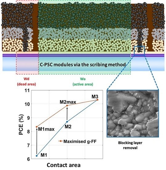
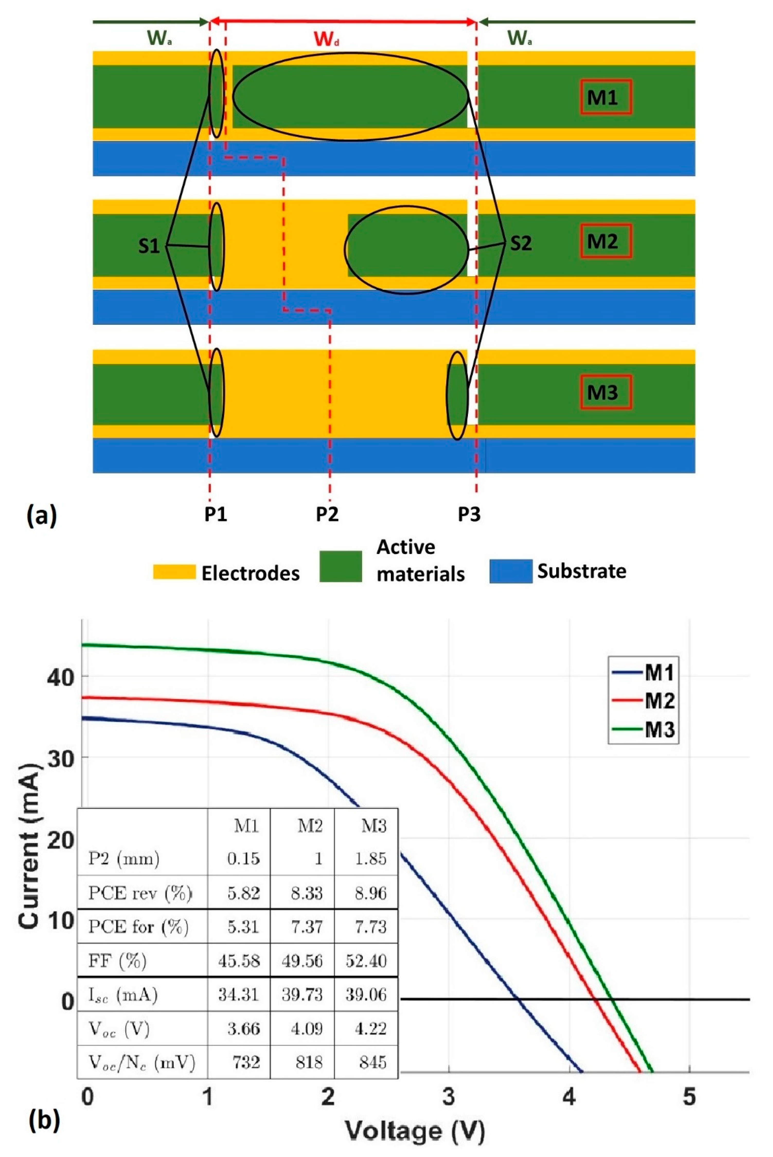
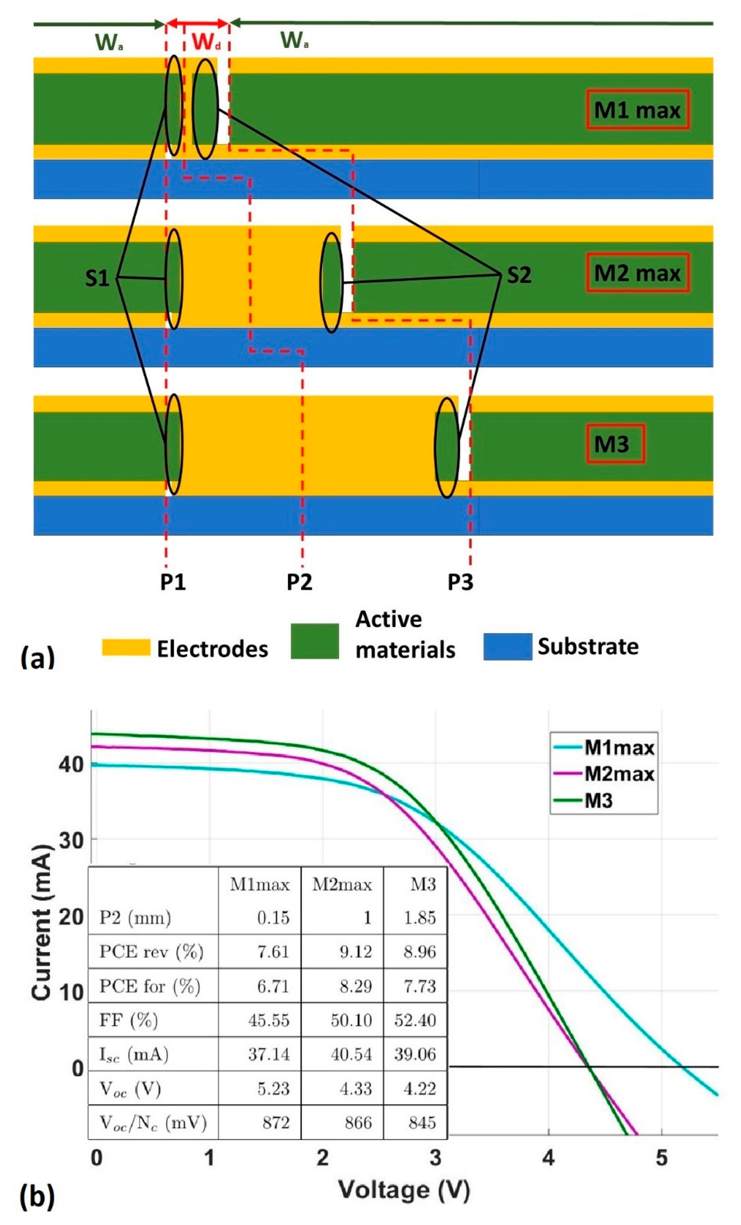
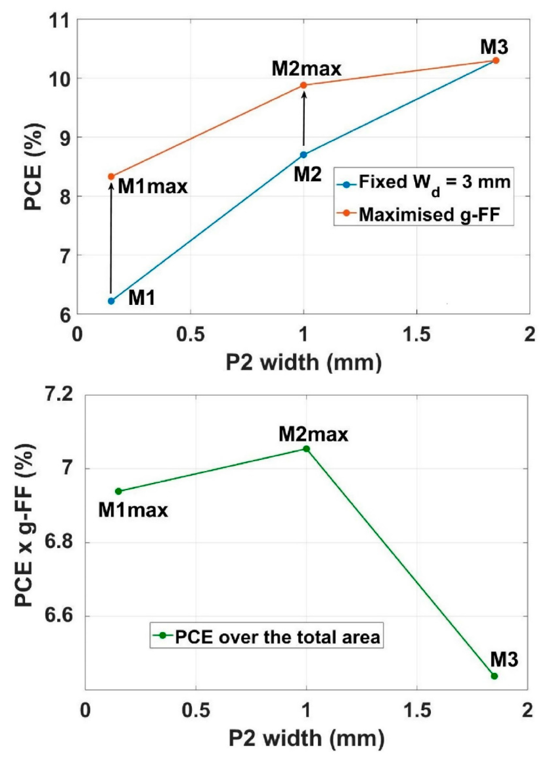
  • the active area width (Wa), which is the result of a trade-off between PCE and the g-FF [18];
  • the dead area width (Wd) or distance between the cells, which is limited by the manufacture method that is adopted and the contact area width;
  • the contact area width, which reduces the contact resistance (Rc) but limits the minimization of the Wd.
An alternative method to create interconnects is based on a material removal approach, known as the scribing method. Here, three different scribes, or patterns, are applied on different layers of the device to make the interconnects. With this method, high g-FF can be achieved for architectures that employ metal top contacts, e.g., below 80% [19], around 85% [20] or even more than 90% [21,22,23]. Furthermore, the scribing method is particularly suitable for large area productions because it can be used in either sheet-to-sheet or roll-to-roll processes [16]. These scribes are called P1, on the bottom electrode, P2, on the active layers, and P3, on the top electrode. The sequence and the location of each scribe for the C-PSC architecture is shown in Figure 1a–e. To achieve high quality interconnects with low resistance, the mechanical scribing method requires clean and selective scribes through multiple layers. Incomplete material removal may cause shorts between cells (for P1 and P3) or a reduced contact area where carbon can physically contact FTO (for P2). An excess of material removal, on the other hand, may cause fragility in the substrate, especially during thermal cycles (for P1), decreased electrode conductivity or, even worse, electrical insulation between cells (for P2 and P3). The P1 and P3 scribes define the active and dead areas of the device, whereas the P2 scribe ensure the connection in series between the cells. The areas between P1 and P2, P2 and P3 are called, respectively, S1 and S2 (space 1 and space 2, Figure 1e). The use of the scribing method reduces the need of extra-spaces that simplify the registration of layers, as shown in Figure 2.
Special attention should be paid to the P2, which determines the contact between cells. The P2 must be selective, to not damage the FTO, and complete, to remove all the layers including the bLayer. The removal of the bLayer allows a direct contact between the carbon top electrode and the FTO [17,24]. This material removal of the bLayer reduces the waste in space to make the interconnects because the patterning matches exactly the contact area. This approach has been already proved for mechanical scribing on soft layered material, such as TiO2/perovskite/Spiro OMeTAD [21,25]. Another key aspect of the P2 scribe is the contact area width. The contact area is defined by the width of the P2 scribe. When the P2 scribe is increased in width, the contact area is enlarged with a consequent improvement in electrical contact between adjacent cells. However, a large P2 implies also a larger distance between cells, negatively affecting the g-FF. In the more common PSC architectures with a metal top electrode, the P2 size can be as narrow as 150–200 µm [22]. When porous and less conductive layers are used, such as carbon in case of C-PSC, the size of the contact can be expected to be larger.
In order to maximise the g-FF, the scribing approach was utilised to fabricate C-PSC modules for the first time in this work. Laser was used to prepare the substrate (P1 of FTO) and mechanical removal was utilised for the further scribes (P2 and P3). The role of the contact area on the performance of modules was investigated and devices with increasing g-FF and PCE up to 10% were demonstrated. Here, an optimised P2 size to maximise the product of module performance and g-FF will be presented, showing the key role of the FTO/carbon interconnect and the distance between the scribes, i.e., S1 and S2. The optimal design found in this set of experiments was, then, used to prepare a 10 × 10 cm2 module, which shows comparable performance to the 5 × 5 cm2 modules. The result with the 10 × 10 cm2 module and the use of the scribing method for the C-PSC have the potential to unlock large scale industrial production of perovskite solar cells with low-capital cost.

2. Materials and Methods

2.1. Materials

The following solvents and reagents were used: PbI2 (99.99%, TCI), methylammonium iodide (MAI, Dyesol), γ-butyrolactone (GBL, 99.8%, Sigma-Aldrich), 5-aminovaleric acid iodide (5-AVAI, Dyesol), carbon paste (Gwent electronic materials), ZrO2 paste (Solaronix), TiO2 paste (30NR-D, Dyesol), terpineol (95%, Sigma-Aldrich), 2-propanol (IPA, 98%, Fisher Scientific) and titanium diisopropoxide bis(acetylacetonate) (TAA, 75%, Sigma-Aldrich). Conductive fluorine-doped tin oxide glass (FTO, TEC-7, XOP) was used as substrate.

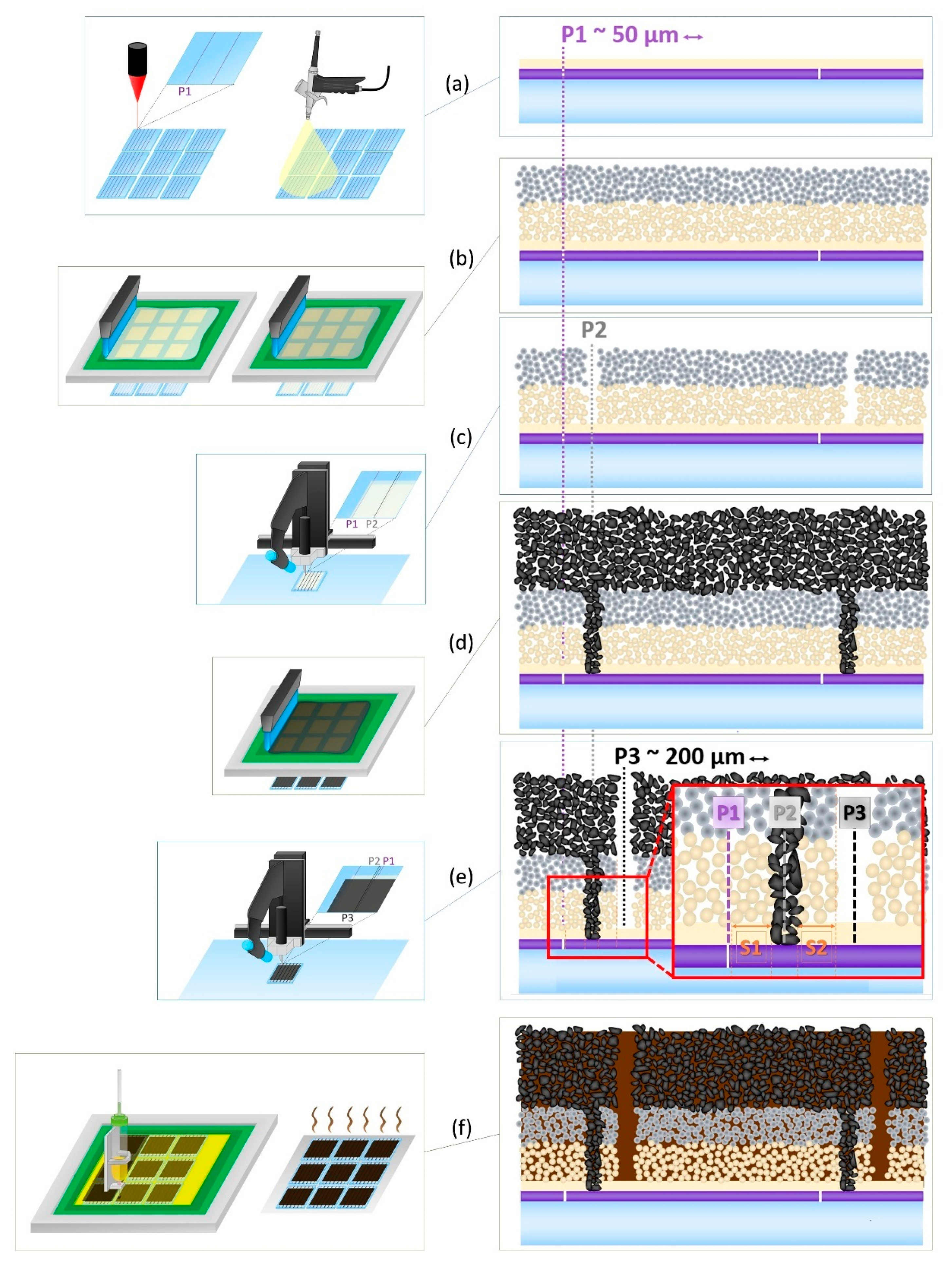
2.2. Device Fabrication

The P1 scribe on FTO was carried out using a Nd:YVO4 laser (diode end-pumped, 532 nm wavelength, pulsed at 50 kHz, average output power 30 W at 170 mm/s, pulse width 10.0 µs). The cleaning of the substrate, deposition of the compact TiO2 (bLayer) by spray (solution of TAA in IPA 10% vol), the screen-printing of the mesoporous TiO2, ZrO2 and carbon layers, and the relative annealing processes, followed our previous work [26]. The thickness of the mesoporous layers was around 0.8, 1.2, and 12 µm for TiO2, ZrO2, and carbon, respectively. The variation of the thickness depends on the screen-printing parameters, and the more difficult to control is the pressure of the squeegee. For a proper reproducibility of the process, it is important to control the thickness for each batch of prints. The AVA-MAPI precursors solution was prepared with 439.0 mg, 151.4 mg, and 6.7 mg of, respectively, PbI2, MAI, and 5-AVAI in 1 mL of GBL. The solution was then deposited with the so-called Robotic Mesh (RbM) method [26]. In this RbM method, a robotic dispenser moves a syringe to continuously deliver the precursor solution at 12 m/s to a mesh which is on the top of the device to homogeneously spread the liquid on the surface. The wet devices were kept in a closed Petri dish for 10 min at room temperature and then heated at 50 °C in oven. After 60 minutes, the Petri dish was opened, and the devices were left in the oven for another hour to complete the drying step. The devices were then placed in a humidity oven at 70% RH and 25 °C for 24 hours [17]. The scribes were made mechanically with a steel blade for the P2 and P3 scribes as shown in Figure 1. The material removal occurred with an automated X-Y stage. The blade is attached to a 31 mm steel alloy spring which can be compressed to 0.54 N/mm. A compression of 14 mm (for P2) and 5 mm (for P3) was applied. P2 was either scribed with a single passage (or with two separate lines for the 1 and 1.85 mm contacts) at a given distance apart with the interspace material manually removed with a blade.

2.3. Characterization

IV measurements were carried out using a Newport Oriel solar simulator (class AAA) calibrated with a KG5 filtered silicon reference cell. A Keithley 2400 source meter was used at a scan rate of 200 mV/s between −0.2 V and 5 V for the 5-cells, or 6 V for 6 cells, in forward and reverse directions after 3 min light soaking. The active area was defined by the width and length of each cell multiplied by the number of cells. Raman measurements were performed with a Renishaw Invia Raman system in backscattering configuration. A laser excitation of 532 nm, and a 50× long objective was used. Raman maps were obtained by measuring several points of the sample with an X-Y scanning stage. The maximal intensity of spectra in the Raman shift in the range of the observed peak over the baseline was used to determine the signal intensity. The measurements were carried out through the glass side. Scanning electron microscopy was obtained using a Hitachi tabletop microscope TM3030 with EDX Quantax70 (SEM/EDX) for lower resolution, rapid imaging. Cross-sections were prepared after lass cutting using a Hitachi IM4000 Plus Ar broad beam ion miller with a probe current of 4 kV for 1.5 h. Samples were mounted onto a conductive holder and coated in 5 nm Pt to provide conductivity for the glass substrate. Imaging was undertaken on a Jeol JSM-7800F FEG-SEM at 15 kV using secondary electron imaging, with EDX analysis provided using an Oxford Instruments detector. XRD measurements were carried out using a Bruker diffractometer with Bragg-Brentano geometry. Cu kα radiation was applied as X-ray source. Scans in 2θ were collected using a step size of 0.01°.

3. Results and Discussion

The conductive glass substrate can be patterned with the laser to obtain a P1 scribe of just above 50 µm wide, as it was already reported [17,26]. The process is very well established and enables quick patterning of the FTO without damaging the glass substrate. This is ideal for the preparation of a substrate that will be exposed to a significant thermal stress during the fabrication process.
After the deposition of the bLayer all over the substrate, a functionalized and patterned substrate is obtained. Once the glass/patterned FTO/bLayer substrate is ready, the next manufacture steps are based on the low-capital cost screen-printing and mechanical scribing methods. The scribes through the screen-printed layers will be discussed below.

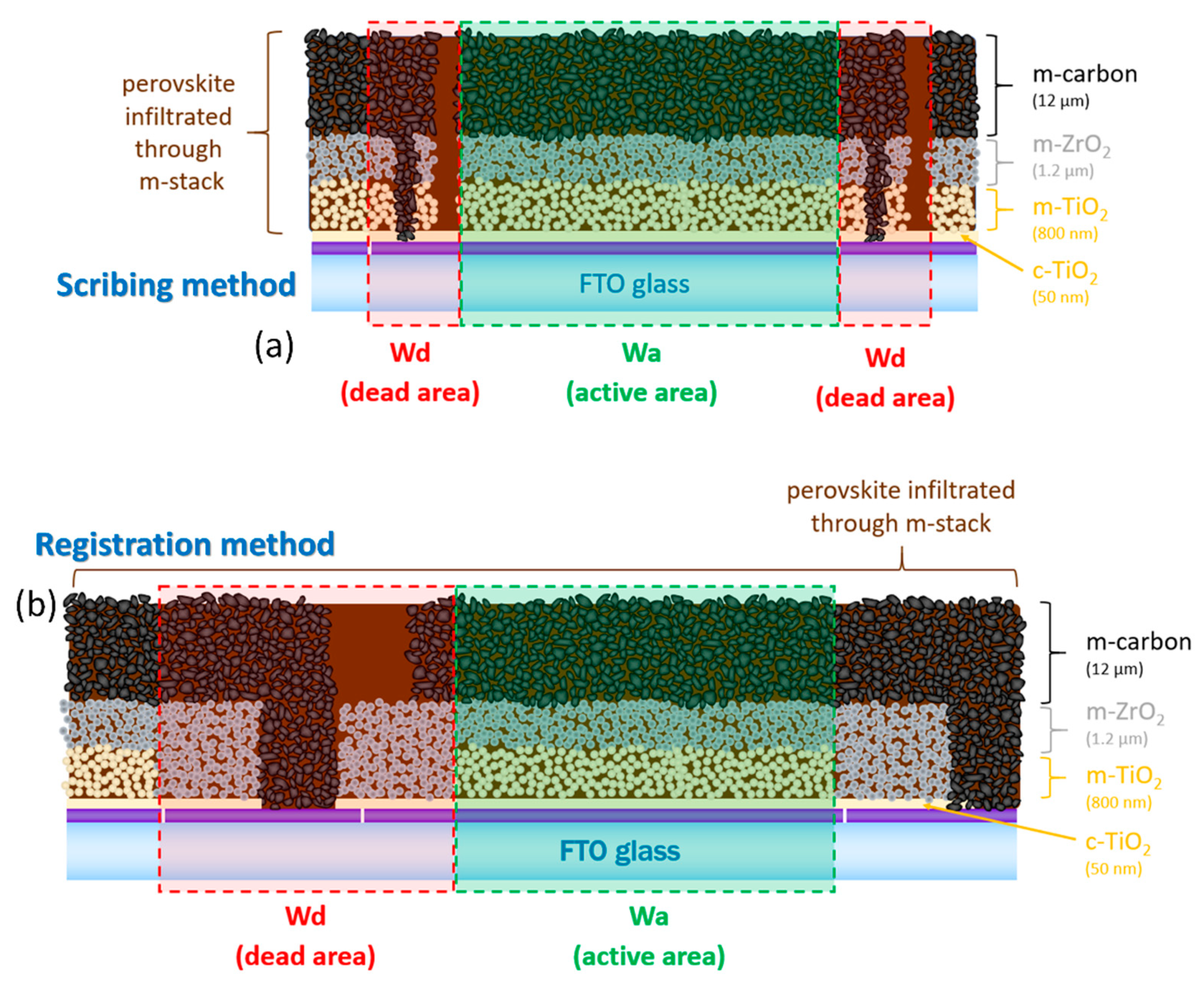
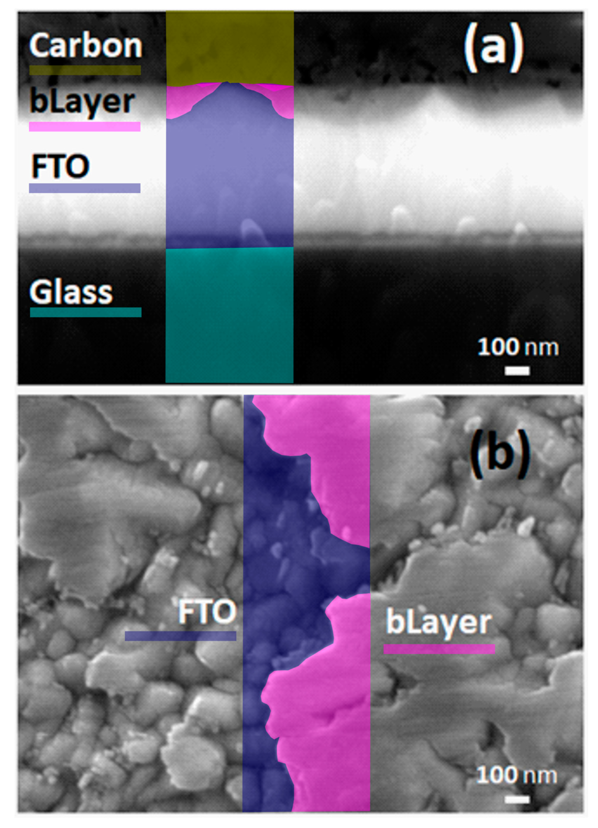
3.1. P2: TiO2/ZrO2 Removal

Mechanical scribing of the P2 is performed using a metal blade after the deposition and heating of the mTiO2 and mZrO2 layers. The P2 could be made with the same green laser that is used for the P1, as reported for other architectures [22]. However, perovskite is not infiltrated in the C-PSC at this stage, thus, no material can absorb visible light and protect the FTO layer. Furthermore, the combined use of screen-printing and mechanical scribing unlocks the possibility to produce modules in large scale with low-capital cost. This is because functionalized glass substrates with patterned FTO and bLayer are commercially available [27], whereas the further layer depositions of mTiO2, mZrO2 and carbon and the relative P2 and P3 scribes can be carried out via inexpensive techniques, i.e., screen-printing and mechanical scribing.
The selectivity of the material removal is ensured mostly by the hardness of the blade in the mechanical approach. A metal (steel) tip can be adopted without affecting the FTO layer for a complete material removal, including the bLayer [21,25]. The tip of the blade is scraped along the device surface creating the P2 scribe. The P2 scribe removes both the mTiO2 and mZrO2 as well as the underlying bLayer, creating an aperture for the final deposited carbon layer to contact with the FTO of the next cell. It is crucial that this scribe completely removes all the layers but not FTO, which is the bottom electrode of the adjacent cell (Figure 1c,d). The P2 scribe must be as close as possible to the P1, but a safe S1 area is necessary to avoid any overlapping and, thus, the possibility of any short circuit between cells. The positioning of the P2 scribe is a trade-off between maximising the g-FF and ensuring the interconnects are large enough to ensure proper electric contact between adjacent cells.
Raman and EDX mapping were used to verify the successful removal of material in the P2 scribe. The Raman signal of TiO2 (peak at 144 cm−1) [28] was used to monitor the material removal, because ZrO2 does not show any characteristic peak (for the characterization of each layer by XRD and Raman, Figure S1). Raman and EDX show that the scribe completely removes the mesoporous layers but not the FTO layer (Figure S2), making the scribe suitable for creating interconnects. Furthermore, the bLayer appears removed, or partially removed, in the Raman analysis (Figure S2). This is observed by high resolution SEM. The cross-sectional image (Figure 3a) shows that the FTO is in direct contact with the carbon layer while only partial bLayer material remains trapped in the roughness of the FTO surface. This is further confirmed by the top view of a glass/FTO/bLayer sample after mechanical scribing, where the FTO appears completely free from the bLayer (Figure 3b). At this stage, it is possible to proceed with the P3 scribe.

3.2. P3: TiO2/ZrO2/carbon Removal

The P3 scribe penetrates the porous layers and defines, with the P1 scribe, the single cell active and dead width (Wa, Wd, Figure 1e). The scribe is a balance between achieving complete material removal and ensuring a sufficiently narrow line to maximise the g-FF. Since the P3 scribe must not damage the underlying FTO layer, the mechanical scribing approach with metal blade can be used, as already observed for the P2 scribe. Therefore, a similar approach based on the use of a metallic scriber was used for a P3 scribe of around 200 µm wide (Figure S3), making possible the manufacture of the modules via low-capital cost methods. After the P3, the stack can be infiltrated with AVA-MAPI solution to complete the module fabrication.

3.3. Module Design: the Effect of the Contact Area

In series connected modules, the contact resistance (Rc) of the interconnects between adjacent cells links the series resistance (Rs) component of the individual cells, as shown in Figure S4. In a typical architecture with a metal top electrode, the effect of Rc can be negligible due to the higher conductivity of metals over porous carbon, and tiny P2 scribes can ensure enough low Rc. Due to the resistance of carbon and its porosity, which reduces the effective contact area between cells, the required width of the P2 scribe to achieve efficient C-PSC modules can be relatively large. To explore the influence of the P2 width on the module PCE, a set of modules was prepared using three different widths: 0.15 mm (similar to the P2 scribe employed for metal contacts), 1 mm and 1.85 mm. The P1 and P3 scribes were kept fixed at around 50 µm and 200 µm, respectively. The complete cell-to-cell distance was fixed to 3 mm for all P2 widths. This width was set to fit even the larger scribe and avoid any variation of the other design parameters. As the only variable is the P2 width, which is included in the fixed dead area Wd, the g-FF does not change (62.5%), as well as the cell number (Nc), for all the different module layouts. These modules are named M1, M2, and M3 (Table 1, Figure 4a and Figure S5a–c). The optimisation of the g-FF will be discussed in the next section.
The power conversion efficiency (PCE) increases when the P2 scribe is enlarged, from the M1 to the M3 layouts (Figure 4b, Table S1 and Figure S6). On average, the PCE increases from around 5.8% to 8.3% from M1 to M2 and goes to 8.9% from M2 to M3. The Isc increases slightly from M1 to M2 (from 34.3 mA to 39.7 mA) but it remains roughly constant from M2 to M3 (39.7 and 39.1 mA, respectively). The use of larger contact areas at the interconnects is beneficial especially on the fill factor (FF). The FF is strongly affected by both the Rs and the Rc, but only the Rc can vary in these sets of modules because the cell-to-cell distance is kept constant. The average FF is 45.6% for M1 modules, it increases in M2, 49.6%, and continues to grow in the M3 modules, to 52.4%. The improvement in FF that is observed with the increase in the P2 size width is a strong sign of a decrease in the Rc that is added in the total resistance in the device. The open circuit voltage Voc increases with the increase in the P2 size. The Voc of a series connected module is the sum of the Voc of each cell. The averaged Voc of the cells (Voc/Nc) is as follows: 732 mV for M1, 819 mV for M2 and 845 mV for M3. The observed trends, especially the Voc/Nc, can be further discussed alongside the results that will be presented in the next section.

3.4. Module Design: Geometric Fill Factor Optimisation

The previous section showed that a wider P2 scribe improves the C-PSC module performance when Wd is constant. Further improvements in PCE can be made by decreasing the Wd, which decreases the current path, thus the Rs, with a consequent increase in g-FF. A set of modules was prepared with the aim of exceeding 62.5% g-FF, demonstrated previously, by modifying the M1 and M2 layouts. However, the reduction in Wd is limited by the size of the P2 width and, for a given P2, a different g-FF can be achieved. A detailed schematic of each module layout can be found in Figure 5a and Figure S5d–f. Keeping Wa constant and equal to 5 mm, two module designs were tested, namely M1max (P2 = 0.15 mm, Wd = 1 mm) and M2max (P2 = 1 mm, Wd = 2 mm). The primary purpose of these new modules (M1max and M2max) were to investigate the effect of reducing the dead area (Wd) whilst keeping both the active area (Wa) and the P2 scribe width the same as the original designs (M1 and M2). These modules were also compared with M3.
The modules improve significantly with minimisation of Wd. Considering the averaged values of each set of modules, M1 improves from 5.8% (Wd = 3 mm) to 7.6% of M1max (Wd = 1 mm), whereas M2 goes from 8.3% (Wd = 3 mm) to 9.1% of M2max (Wd = 2 mm). The improvement can be mostly attributed to the reduced distance between cells and the relative effect on Rs. It is expected, therefore an improvement in FF, as it can be modelled with a simple diode equation. However, the FF does not change significantly when the Wd is minimised. The FF of M1 and M1max are both around 45.5%, while M2 and M2max are 50%, reflecting the effect of the improved contact area when the P2 size is increase, as discussed previously and not the reduction in the cell-to-cell distance.
High Rs and Rc can affect Isc when it is particularly high. The Isc is comparable between M1max, M2max and M3, in spite of the trend observed for M1, M2 and M3. In detail, the Isc of M2 was similar to that to M3 as well as M2max. The only set of modules that presented a striking low Isc was M1, which was 3 mA lower than M1max according to the averaged values (from 34.3 to 37.1 mA/cm2). The low Isc could reflect the internal resistance which is particularly high in the M1 layout, due to the small contact area and the large cell-to-cell distance. The reduction in Wd could partially compensates the poor contact with the narrow P2 scribe, resulting in a comparable overall effect on Rs overall when compared to the M1max layout. The Voc increased significantly when the cells were brought closer together. The improvement in Voc/Nc from M1 to M1max was by 140 mV. The same trend was observed from M2 to M2max, where the improvement was around 50 mV. It should be noted that Voc/Nc was comparable in M1max, M2max, and M3 modules, i.e., when Wd was reduced for the relative P2 width.
In this case the width of the P2 scribe, related to Rc, balanced out the reduction in Wd, which is related to Rs. However, Voc should not be affected by Rs but by recombination phenomena [29]. The fact that the Voc improved with the increase in the P2 scribe and the decrease in the Wd may have different reasons. The size of the S2 area was very different for M1, M2 and M3 layouts, but was comparable for M1max, M2max and M2, as described in Table 1 and Table 2, and shown in Figure 4a and Figure 5a. S1 and S2 are the spaces between the scribes and might act as active cells that generate current, but are not connected in series with the principal cells of the device. This current generation might cause recombination and, therefore, a reduction in Voc. The mechanism might not be negligible when S1 and S2 are large, as in the case of M1 and M2 modules. The minimisation of S1 and S2 is beneficial for the minimisation of the recombination phenomena. In other words, the reduction in Wd has multiple effects on the module performance, including the reduction in recombination phenomena occurring in the areas between the scribes.
It was observed that the minimisation of the Wd and a large P2 improves the device performance. However, g-FF depends on Wd. The PCE × g-FF is the main parameter when considering the performance of a module. In the case of M3 modules, the g-FF is 62.5%, which nearly halves the PCE × g-FF product. Much higher g-FF is for M1max, i.e., 83.3%, but the PCE is not as high as M2max and M3. M2max modules have comparable performance to M3 and the g-FF is 71.4% and it represents the optimal design in terms of PCE × g-FF in this set of experiments (Figure 6).
The M2max layout was adopted to prepare a 10 × 10 cm2 device with 12 cells connected in series and 84 mm long (P2 = 1 mm, Wd = 2 mm, Wa = 5 mm). Regardless of the increasing size of the device, the same design shows comparable performance from the 5 × 5 cm2 to the 10 × 10 cm2, i.e., 10.37% (Figure 7). This result demonstrates that the C-PSC modules can be easily scaled-up when homogeneous and defect-free layers can be deposited.

4. Conclusions

Series connected triple mesoscopic C-PSC modules were successfully prepared by scribing for the first time. The champion modules reached 10.29% PCE on 5 × 5 cm2 and 10.37% PCE on 10 × 10 cm2. The scribes to create the interconnects were characterized, showing the possibility of removing the compact TiO2 layer (bLayer) mechanically at the contact area. The results showed that a critical element in achieving appropriate interconnects is the contact resistance at the FTO/carbon interface. The poor conductivity of the porous carbon layer, compared to typical metal contacts, can be compensated with a slightly larger contact area. The g-FF can be maximised with the reduction in safe space between the scribes. This increases the generated power of the device, especially due to the Voc. The possibility that the safe areas between the scribes (S1 and S2) can affect the recombination was discussed. An optimal design that maximises both PCE and g-FF should consider the use of a P2 width of the order of hundreds of µm and the minimization of the safe spaces S1 and S2. The comparable performance between the 5 × 5 cm2 and 10 × 10 cm2 modules demonstrates the simplicity of up-scaling C-PSC. The combined use of screen-printing and scribing methods on pre-fabricated patterned substrates can unlock the possibility of fabricating perovskite solar modules with low-capital cost.

Supplementary Materials

The following are available online at https://www.mdpi.com/1996-1073/13/7/1589/s1, Figure S1: Characterization of each layer of the C-PSC stack after the sequential deposition on the same substrate by XRD and Raman. Figure S2: P2 characterization. Figure S3: P3 characterization. Figure S4: Equivalent circuit of a 2-cell series connected module. Figure S5: Dimensions of the modules. Figure S6: Statistical analysis of JV data. Table S1: Measured data from JV measurement of the modules under study.

Author Contributions

Conceptualization, S.M.P.M. and T.M.W.; Data curation, S.M.P.M.; Formal analysis, S.M.P.M., K.E.A.H., T.D., J.A.B. and C.C.; Funding acquisition, D.W. and T.M.W.; Supervision, D.W., C.C. and T.M.W.; Writing—original draft, S.M.P.M.; Writing—review & editing, K.E.A.H., T.D., D.W., C.C. and T.M.W. All authors have read and agreed to the published version of the manuscript.

Funding

This work was made possible by support from the UKRI Global Challenge Research Fund project SUNRISE (EP/P032591/1) and through the funding of the SPECIFIC Innovation and Knowledge Centre by the Engineering and Physical Science Research Council [EP/N020863/1], Innovate UK [920036], and the European Regional Development Fund [c80892] through the Welsh Government. This work was supported by a an institutional links grant, ID 332397170, under the Newton Mexico partnership. The grant is funded by the UK. We would also like to acknowledge the assistance provided by Swansea University College of Engineering AIM Facility, which was funded in part by the EPSRC (EP/M028267/1), the European Regional Development Fund through the Welsh Government (80708) and the Ser Solar project via Welsh Government.

Conflicts of Interest

The authors declare no conflict of interest.

References

  1. Kojima, A.; Teshima, K.; Shirai, Y.; Miyasaka, T. Organometal halide perovskites as visible-light sensitizers for photovoltaic cells. J. Am. Chem. Soc. 2009, 131, 6050–6051. [Google Scholar] [CrossRef] [PubMed]
  2. Liu, M.; Johnston, M.B.; Snaith, H.J. Efficient planar heterojunction perovskite solar cells by vapour deposition. Nature 2013, 501, 395–398. [Google Scholar] [CrossRef] [PubMed]
  3. Baikie, T.; Fang, Y.; Kadro, J.M.; Schreyer, M.; Wei, F.; Mhaisalkar, S.; Graetzel, M.; White, T.J. Synthesis and crystal chemistry of the hybrid perovskite (CH3NH3)PbI3 for solid-state sensitised solar cell applications. J. Mater. Chem. A 2013, 1, 5628. [Google Scholar] [CrossRef]
  4. Ku, Z.; Rong, Y.; Xu, M.; Liu, T.; Han, H. Full Printable Processed Mesoscopic CH3NH3PbI3/TiO2 Heterojunction Solar Cells with Carbon Counter Electrode. Sci. Rep. 2013, 3, 3132. [Google Scholar] [CrossRef] [Green Version]
  5. Chen, H.; Yang, S. Carbon-Based Perovskite Solar Cells without Hole Transport Materials: The Front Runner to the Market? Adv. Mater. 2017, 29, 1603994. [Google Scholar] [CrossRef]
  6. Li, X.; Tschumi, M.; Han, H.; Babkair, S.S.; Alzubaydi, R.A.; Ansari, A.A.; Habib, S.S.; Nazeeruddin, M.K.; Zakeeruddin, S.M.; Grätzel, M. Outdoor Performance and Stability under Elevated Temperatures and Long-Term Light Soaking of Triple-Layer Mesoporous Perovskite Photovoltaics. Energy Technol. 2015, 3, 551–555. [Google Scholar] [CrossRef]
  7. Grancini, G.; Roldán-Carmona, C.; Zimmermann, I.; Mosconi, E.; Lee, X.; Martineau, D.; Narbey, S.; Oswald, F.; De Angelis, F.; Graetzel, M.; et al. One-Year stable perovskite solar cells by 2D/3D interface engineering. Nat. Commun. 2017, 8, 15684. [Google Scholar] [CrossRef]
  8. Baker, J.; Hooper, K.; Meroni, S.M.P.; Pockett, A.; McGettrick, J.; Wei, Z.; Escalante, R.; Oskam, G.; Carnie, M.J.; Watson, T. High throughput fabrication of mesoporous carbon perovskite solar cells. J. Mater. Chem. A 2017, 5, 18643–18650. [Google Scholar] [CrossRef] [Green Version]
  9. Péan, E.V.; De Castro, C.S.; Dimitrov, S.; De Rossi, F.; Meroni, S.; Baker, J.; Watson, T.; Davies, M.L. Investigating the Superoxide Formation and Stability in Mesoporous Carbon Perovskite Solar Cells with an Aminovaleric Acid Additive. Adv. Funct. Mater. 2020, 30, 1909839. [Google Scholar] [CrossRef] [Green Version]
  10. Liu, L.; Mei, A.; Liu, T.; Jiang, P.; Sheng, Y.; Zhang, L.; Han, H. Fully Printable Mesoscopic Perovskite Solar Cells with Organic Silane Self-Assembled Monolayer. J. Am. Chem. Soc. 2015, 137, 1790–1793. [Google Scholar] [CrossRef]
  11. Tian, C.; Mei, A.; Zhang, S.; Tian, H.; Liu, S.; Qin, F.; Xiong, Y.; Rong, Y.; Hu, Y.; Zhou, Y.; et al. Oxygen management in carbon electrode for high-performance printable perovskite solar cells. Nano Energy 2018, 53, 160–167. [Google Scholar] [CrossRef]
  12. Liu, S.; Huang, W.; Liao, P.; Pootrakulchote, N.; Li, H.; Lu, J.; Li, J.; Huang, F.; Shai, X.; Zhao, X.; et al. 17% efficient printable mesoscopic PIN metal oxide framework perovskite solar cells using cesium-containing triple cation perovskite. J. Mater. Chem. A 2017, 5, 22952–22958. [Google Scholar] [CrossRef]
  13. Yates, H.; Meroni, S.; Raptis, D.; Hodgkinson, J.; Watson, T. Flame assisted chemical vapour deposition NiO hole transport layers for mesoporous carbon perovskite cells. J. Mater. Chem. C 2019, in press. [Google Scholar] [CrossRef] [Green Version]
  14. Yates, H.M.; Hodgkinson, J.L.; Meroni, S.M.P.; Richards, D.; Watson, T.M. Flame Assisted Chemical Vapour Deposition of NiO hole transport layers for planar perovskite cells. Surf. Coat. Technol. 2020, 385, 125423. [Google Scholar] [CrossRef]
  15. Priyadarshi, A.; Haur, L.J.; Fu, D.; Kulkarni, S.; Xing, G.; Mhaisalkar, S.; Murray, P.; Sum, T.C.; Mathews, N. A large area (70 cm2) monolithic perovskite solar module with a high efficiency and stability. Energy Environ. Sci. 2016, 9, 3687–3692. [Google Scholar] [CrossRef]
  16. Hu, Y.; Si, S.; Mei, A.; Rong, Y.; Liu, H.; Li, X.; Han, H. Stable Large-Area (10 × 10 cm2) Printable Mesoscopic Perovskite Module Exceeding 10% Efficiency. Sol. RRL 2017, 1, 1600019. [Google Scholar] [CrossRef]
  17. De Rossi, F.; Baker, J.; Beynon, D.; Hooper, K.; Meroni, S.M.P.; Williams, D.; Wei, Z.; Yasin, A.; Charbonneau, C.; Jewell, E.; et al. All Printable Perovskite Solar Modules with 198 cm2 Active Area and Over 6% Efficiency. Adv. Mater. Technol. 2018, 3, 1800156. [Google Scholar] [CrossRef] [Green Version]
  18. Mouhamad, Y.; Meroni, S.M.P.; De Rossi, F.; Baker, J.; Watson, T.; Searle, J.; Jewell, E. Geometrical optimization for high efficiency carbon perovskite modules. Sol. Energy 2019, 187, 129–136. [Google Scholar] [CrossRef]
  19. Razza, S.; Di Giacomo, F.; Matteocci, F.; Cinà, L.; Palma, A.L.; Casaluci, S.; Cameron, P.J.; D’Epifanio, A.; Licoccia, S.; Reale, A.; et al. Perovskite solar cells and large area modules (100 cm2) based on an air flow-assisted PbI2blade coating deposition process. J. Power Sources 2015, 277, 286–291. [Google Scholar] [CrossRef]
  20. Moon, S.J.; Yum, J.-H.; Lofgren, L.; Walter, A.; Sansonnens, L.; Benkhaira, M.; Nicolay, S.; Bailat, J.; Ballif, C. Laser-scribing patterning for the production of organometallic halide perovskite solar modules. IEEE J. Photovolt. 2015, 5, 1087–1092. [Google Scholar] [CrossRef]
  21. Rakocevic, L.; Gehlhaar, R.; Merckx, T.; Qiu, W.; Paetzold, U.W.; Fledderus, H.; Poortmans, J. Interconnection Optimization for Highly Efficient Perovskite Modules. IEEE J. Photovolt. 2017, 7, 404–408. [Google Scholar] [CrossRef]
  22. Palma, A.L.; Matteocci, F.; Agresti, A.; Pescetelli, S.; Calabro, E.; Vesce, L.; Christiansen, S.; Schmidt, M.; Di Carlo, A. Laser-Patterning Engineering for Perovskite Solar Modules with 95% Aperture Ratio. IEEE J. Photovolt. 2017, 7, 1674–1680. [Google Scholar] [CrossRef]
  23. Calabrò, E.; Matteocci, F.; Palma, A.L.; Vesce, L.; Taheri, B.; Carlini, L.; Pis, I.; Nappini, S.; Dagar, J.; Battocchio, C.; et al. Low temperature, solution-processed perovskite solar cells and modules with an aperture area efficiency of 11%. Sol. Energy Mater. Sol. Cells 2018, 185, 136–144. [Google Scholar] [CrossRef]
  24. Matteocci, F.; Cinà, L.; Di Giacomo, F.; Razza, S.; Palma, A.L.; Guidobaldi, A.; D’Epifanio, A.; Licoccia, S.; Brown, T.M.; Reale, A.; et al. High efficiency photovoltaic module based on mesoscopic organometal halide perovskite. Prog. Photovolt. Res. Appl. 2016, 24, 436–445. [Google Scholar] [CrossRef]
  25. Qiu, W.; Merckx, T.; Jaysankar, M.; De La Huerta, C.M.; Rakocevic, L.; Zhang, W.; Paetzold, U.W.; Gehlhaar, R.; Froyen, L.; Poortmans, J.; et al. Pinhole-free perovskite films for efficient solar modules. Energy Environ. Sci. 2016, 9, 484–489. [Google Scholar] [CrossRef]
  26. Meroni, S.M.P.; Mouhamad, Y.; De Rossi, F.; Pockett, A.; Baker, J.; Escalante, R.; Searle, J.; Carnie, M.J.; Jewell, E.; Oskam, G.; et al. Homogeneous and highly controlled deposition of low viscosity inks and application on fully printable perovskite solar cells. Sci. Technol. Adv. Mater. 2018, 19, 1–9. [Google Scholar] [CrossRef] [Green Version]
  27. Smith, B.; Troughton, J.; Lewis, A.; McGettrick, J.; Pockett, A.; Carnie, M.; Charbonneau, C.; Pleydell-Pearce, C.; Searle, J.; Warren, P.; et al. Mass Manufactured Glass Substrates Incorporating Prefabricated Electron Transport Layers for Perovskite Solar Cells. Adv. Mater. Interfaces 2019, 6, 1801773. [Google Scholar] [CrossRef]
  28. Hooper, K.E.A.; Lee, H.K.H.; Newman, M.J.; Meroni, S.M.P.; Baker, J.; Watson, T.; Tsoi, W.C. Probing the degradation and homogeneity of embedded perovskite semiconducting layers in photovoltaic devices by Raman spectroscopy. Phys. Chem. Chem. Phys. 2014, 19, 5246–5253. [Google Scholar] [CrossRef] [Green Version]
  29. Tress, W.; Yavari, M.; Domanski, K.; Yadav, P.; Niesen, B.; Baena, J.P.C.; Hagfeldt, A.; Graetzel, M. Interpretation and evolution of open-circuit voltage, recombination, ideality factor and subgap defect states during reversible light-soaking and irreversible degradation of perovskite solar cells. Energy Environ. Sci. 2018, 11, 151–165. [Google Scholar] [CrossRef]
Figure 1. The carbon perovskite solar cell (C-PSC) module based on the scribing method. (a) P1 on a substrate (fixed at around 50 µm) of glass/FTO/bLayer via laser scribing and, then, deposition of the bLayer. (b) Deposition of mTiO2 and mZrO2 via screen-printing. (c) P2 via mechanical scribing to open an aperture for the interconnects. Three different P2 sizes were tested in this work. (d) Deposition of the top carbon electrode. (e) P3 (fixed at around 200 µm) to insulate the cells in series. In the inset, a magnification of the interconnection area shows the three scribes and the distance between them, i.e., S1 and S2. (f) Perovskite infiltration.
Energies 13 01589 g001
Figure 2. Schematic representation of C-PSC modules prepared with the (a) scribing method and (b) registration method with the same active area width (Wa). The registration method requires extra space to properly register each layer and the minimisation of dead area width (Wd) is limited by the deposition accuracy.
Energies 13 01589 g002
Figure 3. False colour SEM image of the P2 scribe interconnect. (a) Cross-sectional image showing the conductive FTO (bright-blue) in direct contact with the carbon layer (dark-yellow). The remaining bLayer (violet) that cannot be removed mechanically appears trapped in the roughness of the FTO layer. (b) Top view of the scribe showing that the bLayer is partially removed, leaving an open area where the carbon area can enter into contact.
Energies 13 01589 g003
Figure 4. (a) Schematic representation of the interconnection areas for the three modules M1, M2 and M3 with different P2 width and same Wd. (b) Current-voltage characteristic in reverse scan of representative modules with increasing P2 size, 0.15, and 1.85 mm for, respectively, M1, M2, and M3 (Table 1 and Figure S5a–c). The full set of data can be seen in Table S1 and Figure S6. In the inset, the table describing the average values of the device parameters for each kind of device. The full set of data is shown in Table S1.
Energies 13 01589 g004
Figure 5. (a) Schematic representation of the interconnection areas for the three modules M1max, M2max and M3 with different P2 width and minimised Wd. (b) Current-voltage characteristic in reverse scan of representative modules with increasing P2 size and maximised g-FF (M1max, M2max, and M3, Table 2 and Figure S5c–d). In the inset, the table describing the average values of the device parameters for each kind of device. The full set of data are in Table S1 and Figure S6.
Energies 13 01589 g005
Figure 6. Top: The PCE of the best modules with varying P2 size. The modules improve with an increase in the P2 scribe width and minimisation of Wd. Bottom: The PCE over the total area (PCE × g-FF) of the best modules from M1max, M2max, and M3.
Energies 13 01589 g006
Figure 7. The 10 × 10 cm2 module with M2max design. On the left, current-voltage characteristic. In the inset, the table describing the device parameters.
Energies 13 01589 g007
Table 1. Module designs for studying the contact area effect. PCE is the highest of the 3 modules. Full set of data in Table S1.
ModulesP2
mm
g-FF
%
Wa
mm
Wd
mm
S1
mm
S2
mm
NcPCE
%
PCE Average
%
M10.1562.5530.32.356.225.82 ± 0.32
M2162.5530.31.4558.708.33 ± 0.33
M31.8562.5530.30.6510.298.96 ± 0.84
Table 2. Module designs with maximised g-FF at a given P2 width. PCE is the highest of the 3 modules. Full set of data in Table S1.
ModulesP2
mm
g-FF
%
Wa
mm
Wd
mm
S1
mm
S2
mm
NcPCE
%
PCE Average
%
M1max0.1583.3510.30.368.337.61 ± 0.81
M2max171.4520.30.4559.889.12 ± 0.94
M31.8562.5530.30.6510.298.96 ± 0.84

