Abstract
Impedance source converters as single-stage power conversion alternatives can boost and regulate the output voltages of renewable energy sources. Nevertheless, they, also known as Z-source inverters (ZSIs), still suffer from limited voltage gains and higher stresses across the components. To tackle such issues, extra diodes, passive components, and active switches can be utilized in the basic ZSIs. In this paper, a modified switched-quasi-Z-source inverter (S-qZSI) is proposed, which features continuous input currents and high boosting capability to boost output voltage by minor modifications of a prior-art topology. Furthermore, the voltage stress of the active switches is reduced, which contributes to a lower cost. The operation principles are discussed comprehensively. The performance of the proposed ZSI in terms of conversion ratio, voltage gain, and stresses on the power switches and capacitors is benchmarked with selected ZSIs. Finally, simulations and experimental tests substantiate the theoretical analysis and superior performance.
1. Introduction
Impedance source converters have gone through rapid development in the last few decades since the first Z-source inverter (ZSI) proposed by Peng in [1]. It is known that the traditional voltage source inverter (VSI) only has buck characteristics so that it is usually not directly applied in the power conversion applications. That is, a front-end stage is commonly adopted. However, the extra DC–DC converters may lead to higher costs and lower efficiency [2]. Furthermore, the power switches of the VSI may be damaged if the inverter leg is short-circuited due to wrong drive signals. To address these issues, the Z-source network, as shown in Figure 1a, which features buck-boost characteristics, can be adopted. However, the basic ZSI still suffers from certain limitations, such as discontinuous input currents and high voltage stresses across the components. The quasi-ZSI (q-ZSI), as shown in Figure 1b, provides an effective solution to the above limitations [3]. Based on the basic ZSI/qZSI structure, many attempts have been made to enhance the performance of impedance source converters in terms of high boost capability, low voltage stresses across the components, and high efficiency [4,5,6,7,8,9,10,11,12,13,14,15,16,17].
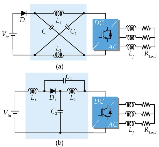
Figure 1.
Circuit schematics of impedance-source-fed three-phase inverters: (a) Z-source inverter [1], and (b) quasi-Z-source inverter [3].
The principle of enhancing the boost capability in the impedance source networks is to add more passive components or power switches into the basic ZSI/qZSI networks. For example, the inductors in the ZSI/qZSI can be replaced by the switched-inductor (SI) cells in Figure 2, in which a higher boost voltage gain can be obtained [8,9,10]. Compared with the SI-ZSI, the SI-qZSI can achieve a continuous input current and lower stresses across the components. Moreover, switched-capacitor (SC) cells can be employed to obtain low voltage stress, small inductors, high voltage gains, and efficiency [11,12].
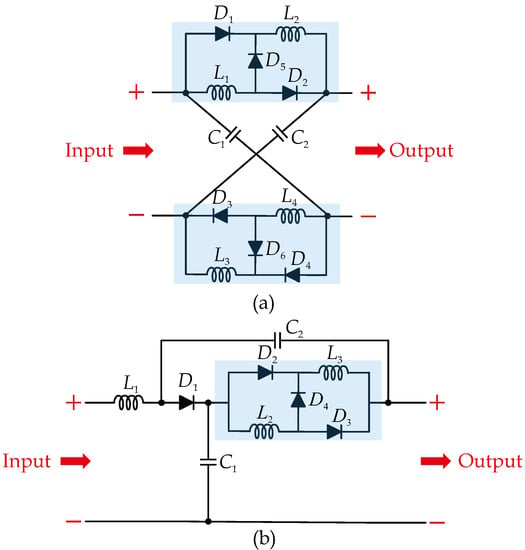
Figure 2.
Modified impedance networks based on switched-inductor: (a) switched-inductor Z-source inverter [8], and (b) switched-inductor quasi-Z-source inverter [9].
Nevertheless, the limitation of these modified converters based on extra components is that many passive devices lead to a higher cost and larger volume of the converter. To tackle this, modified ZSI topologies based on switched-boost networks have been proposed in the literature. The switched-boost inverter (SBI) and embedded-qSBI are shown in Figure 3 [13,14]. The SBI features a lower number of components and the same boost capability by adding one power switch compared to the ZSI. Moreover, the q-SBI and embedded-qSBI have additional advantages, such as reduced voltage stresses on the capacitors, higher voltage gains, and continuous input currents, which makes them appropriate for renewable energy applications. Similarly, the SI or SC cells can be utilized in the SBI/qSBI for a higher boost capability, as presented in [15]. In addition, a diode-assisted SBI (DA-SBI) was proposed in [16]. This modified topology is a combination of the SBI and diode-assisted network, which provides a high voltage gain and continuous input currents. Furthermore, the modified topology quasi-ZSI with continuous input current (CC-qZSI) in [17] shows the improved boost capabilities and less voltage stresses by adding a switched boost network to the original qZSI.
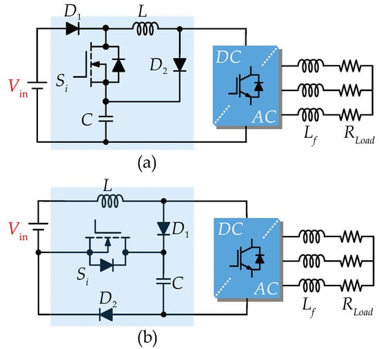
Figure 3.
Impedance-source inverter with active power switches: (a) switched boost inverter (SBI) [13], and (b) embedded-qSBI [14].
Inspired by the above, this paper proposes a modified qZSI with a switched-boost network (S-qZSI), which can achieve continuous input currents and higher boost capability compared with selected switched-boost inverters and modified ZSIs. The rest of this paper is organized as follows. The detailed analysis of the proposed S-qZSI is presented in Section 2. Furthermore, in Section 3, a comprehensive comparison with selected switched-boost ZSIs is carried out and the benchmarking results are provided. The theoretical analysis is verified by simulation and experimental tests in Section 4. Finally, the paper is concluded in Section 5.
2. Operation Principle of the Proposed S-qZSI
The schematic of the proposed S-qZSI is presented in Figure 4. It consists of three capacitors (, , and ), three diodes (, , and ), two inductors ( and ), one power switch (), and a traditional two-level VSI (–). The input voltage is defined as . The voltages across the capacitors (, and ) are defined as , , and , and the diode voltages can be expressed as , , and , and the inductor currents are denoted as and . Moreover, the load current of phase a is defined as .
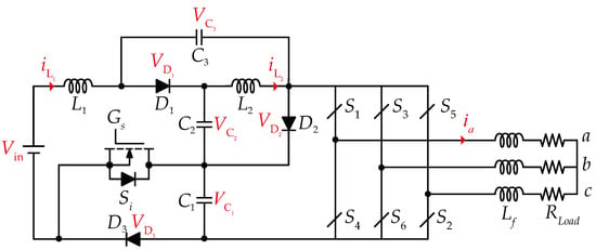
Figure 4.
Schematic of the proposed switched-quasi-Z-source inverter.
Similar to the prior-art ZSIs, the boost capability of the proposed S-qZSI can be achieved by utilizing the shoot-through state of the inverter, in which the inverter leg is short-circuited by turning on two switches simultaneously. Therefore, the operation modes of the proposed S-qZSI can be considered as shoot-through mode and non-shoot-through mode, as presented in Figure 5. The corresponding steady-state waveforms are given in Figure 6. In order to simplify the analysis, the capacitors or inductors in the proposed topology are identical.
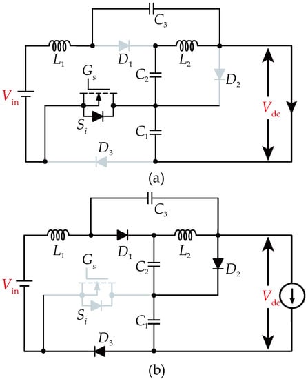
Figure 5.
Operation principles of the proposed S-qZSI: (a) equivalent circuit during the shoot-through state, and (b) equivalent circuit during the non-shoot-through state.
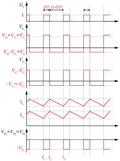
Figure 6.
Steady-state waveforms of the proposed S-qZSI.
As shown in Figure 5a, if the switches in one of the inverter legs receive the same turn-on signal, the inverter side is short-circuited and the DC-link voltage is zero. The power switch is in the conduction state due to the turn-on gate signal , as can be seen in Figure 6. Moreover, the diodes , , and are in OFF-state and the diodes sustain the negative voltage, as presented in Figure 6. Meanwhile, the energy from the input source can be stored in the inductors and the capacitors charge the inductors. Figure 6 shows the inductor currents increase from the minimum to maximum value during the time interval to . On the other hand, Figure 5b shows the non-shoot-through mode and the corresponding time interval is to . In this mode, the operation principle of the inverter is the same as traditional VSI. It can be seen in Figure 6 that the inverter bridge is equivalent to a current source viewed from the DC side [18]. Meanwhile, the switch is turned OFF and the switch voltage is equal to the voltage of the capacitor . Additionally, all three diodes are ON-state and the voltages of the diodes become zero in Figure 6. Moreover, the inductors can release the stored energy to the load or grid side by controlling the inverter switches. That is, the inductor currents decrease from maximum to minimum value as expected in Figure 6. Accordingly, the voltage and currents across the components can be derived by applying the Kirchhoff’s law, as given in Table 1.

Table 1.
Voltage of the components in shoot-through and non-shoot-through modes.
The time intervals in the shoot-through mode and non-shoot-through mode can be expressed as and , where D and T represent the duty cycle and switching period. By applying the volt-second balance principle to the inductors and , the following can be obtained:
where is the peak DC-link voltage. Subsequently, the capacitor voltages can be derived as
Furthermore, and boost factor B can be obtained as
with
being the boost factor. Consequently, the voltage gain G in respect to the modulation index M can be expressed as
3. Comparison with Prior-Art ZSI Topologies
In order to show the performance of the proposed S-qZSI, the component count, boost factor, voltage gain, and component stresses of the proposed S-qZSI and selected topologies are investigated in detail. Firstly, the number of the components in the proposed S-qZSI and selected ZSI topologies is presented in Table 2. According to Table 2, the DA-SBI, CC-qZSI, and the proposed topology all employ two inductors, but the basic SBI and embedded-qSBI only utilize one inductor. Moreover, the quantity of the capacitors in the proposed S-qZSI is higher than the other selected topologies, but it has the same component-count with the DA-ZSI by replacing one diode with a capacitor to construct a quasi-Z-source network.
Table 2.
Comparison of the number of the components in the proposed Sq-ZSI.
Furthermore, Table 3 benchmarks the boost factor, voltage gain, and component stresses among the proposed S-qZSI and selected topologies. Figure 7 compares the boost capability of the proposed topology with other selected ZSI/SBIs. In Figure 7a, the comparison between the duty cycle D and the boost factor B for these topologies is presented. It can be seen in Figure 7a that the basic SBI and embedded-qZSI have relatively lower boost capability due to their small component-count. Furthermore, the boost capability of the DA-SBI and CC-qZSI is greatly enhanced by adding more passive components. It is noteworthy that the proposed S-qZSI can achieve a higher boost factor compared with selected topologies in a certain range of shoot-through duty cycles (i.e., 0–0.3), but the component-count of the proposed topology is the same as that of the DA-SBI. Similarly, Figure 7b shows the relationship between the voltage gain and the modulation index. The proposed S-qZSI has the highest voltage gain among the selected topologies if the modulation indexes are identical within the range of 0.68–1. Therefore, the higher modulation index of the proposed S-qZSI results in better power quality for the same voltage output.
Table 3.
Benchmarking of boost factor, voltage gain, and voltage stresses among selected impedance source inverters.
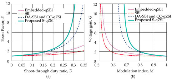
Figure 7.
Comparative analysis: (a) comparison of the boost factor versus the shoot through duty ratio D among the selected topologies, and (b) comparison of the voltage gain versus the modulation index M among the selected topologies.
In addition to the advantage of the high boost capability, as demonstrated above, the proposed S-qZSI can also achieve lower voltage stresses on the power switches. The detailed voltage stresses expressions for the active switch in the network, inverter bridge switch, the capacitors, and the diodes are presented in Table 3. The voltage stress on the components can be defined as the ratio of voltage across the components to . As shown in Figure 8a, the switch stress of the proposed S-qZSI (see in Figure 6) is lower than that of the SBI and DA-SBI, although the component-count of the proposed S-qZSI and DA-SBI is the same. Moreover, it is noteworthy that the ratio of the CC-qZSI for switch stress is a constant value, which means that the ratio is independent of voltage gain and input voltage. As for the stress comparison of inverter bridge switches (–) as presented in Figure 8b and Table 3, the DA-SBI and CC-qZSI have the same inverter bridge switch stress, and the proposed S-qZSI has the best performance compared with other selected topologies, which allow lower ratings of the switches and reduce the cost to some extent. Moreover, Figure 9a compares the capacitor stress. According to Table 3, two of the capacitors in the proposed S-qZSI have the same voltage stress. Moreover, although the proposed topology utilizes one more capacitor, this additional capacitor has low voltage stress compared with other capacitors based on Table 3. Considering all the topologies in Figure 9a, the CC-qZSI has the lowest capacitor voltage among all the topologies, but the proposed S-qZSI shows better performance than the SBI, the embedded-qSBI, and the DA-SBI. Finally, the comparison of diode stress is presented in Figure 9b. Similarly, the diode stress of the proposed S-qZSI is much lower than most of the selected topologies, except the embedded-qSBI.
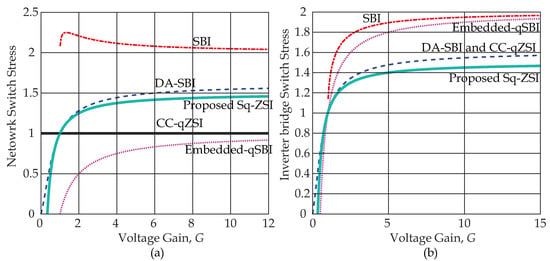
Figure 8.
Switch stress comparison among the selected topologies with various voltage gains: (a) network switch stress comparison, and (b) inverter bridge switch stress comparison.
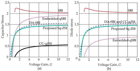
Figure 9.
Stress comparison among the selected topologies with various voltage gains: (a) capacitor () stress comparison, and (b) diode () stress comparison.
4. Simulation and Experimental Results
In this section, simulations and experimental tests are provided to verify the performance of the proposed S-qZSI. As shown in Figure 4, the output stage is achieved by a three-phase system for verification. Table 4 presents the system parameters applied in the simulations and experimental prototype.
Table 4.
Parameters of the proposed S-qZSI.
4.1. Simulation Results
The simulations are executed in the PLECS and Matlab/Simulink platform. The simulation results are given in Figure 10. The output voltage and load current of the whole system are shown in Figure 10a. According to Equation (6), the boost factor B is equal to four when D is 0.25, and thus the DC-link peak voltage can be boosted to 120 V. Figure 10a shows that the DC-link peak voltage is the same as the theoretical value, which equals 120 V. Moreover, the peak load current is about 2 A. Additionally, the DC-link voltage and inductor currents are presented in Figure 10b. It can be seen that the characteristics of the inductor currents match well with the steady-state analysis, where the inductor currents increase during the shoot-through state and decrease during the non-shoot-through state. It can be observed in Figure 10b that the inductor current is continuous DC currents. In Figure 10c, the gate signal and diode voltage , and are presented, where the peak diode voltage is the same as the peak DC-link voltage. Figure 10d presents the capacitor voltage of the proposed topology. The voltage of the capacitor is 120 V, which is equal to the DC-link peak voltage. Moreover, the voltages of the capacitors and are only 30 V, which is consistent with the input DC voltage.
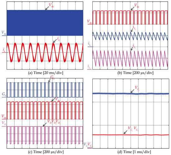
Figure 10.
Simulation results of the proposed S-qZSI: (a) DC-link voltage [50 V/div] and output phase-a current [2 A/div], (b) DC-link voltage [100 V/div] and inductor currents , [5 A/div], (c) gate signal , DC-link voltage [50 V/div] and diode voltages , , [50 V/div], and (d) capacitor voltages , , [50 V/div].
4.2. Experimental Results
The prototype of the proposed S-qZSI is designed based on the previous analysis, as presented in Figure 11. The parameters of the prototype are the same as the parameters applied in the simulations. The control signals applied in the proposed S-qZSI are generated from a digital signal processor (DSP) TMS320F28335 from Texas Instrument and field-programmable gate array (FPGA) Altera Cyclone 4. The DSP is used to generate the complementary signals and the FPGA board can perform the logical operation based on the output signals from the DSP.
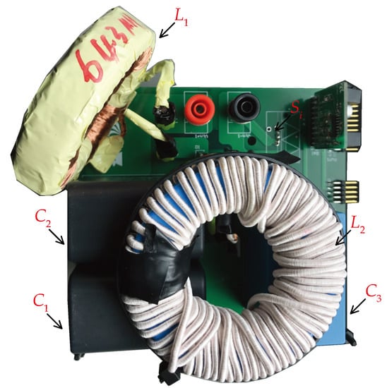
Figure 11.
Photograph of the prototype of the proposed S-qZSI.
Figure 12 presents the experimental results of the proposed S-qZSI under the condition that M is 0.83 and D is 0.25. As shown in Figure 12a, the boosted DC-link voltage is approximately 3.88 times as large as the input voltage (30 V) and the load current is about 1.8 A. It can be observed in Figure 12 that the obtained boost factor from the experimental result is slightly lower than the theoretical value due to the parasitic components associated with diodes, switches, capacitors, or inductors applied in the prototype. Moreover, Figure 12b shows the experimental results for the DC-link voltage and inductor currents. It can be observed in Figure 12b that the inductor currents increase linearly in the shoot-through state and decrease linearly in the non-shoot-through state, which is in correspondence with theoretical analysis and simulation results. Meanwhile, the DC-link voltage is zero in the shoot-through state and nonzero in the non-shoot-through state, which matches well with the simulation results. Furthermore, the continuous input current can be ensured in the proposed topology by observing the inductor current . Additionally, the gate signal and diode voltages are shown in Figure 12c. The peak diode voltage is equal to the peak DC-link voltage. Finally, the capacitor voltages of the proposed topology are shown in Figure 12d. It can be seen that the capacitor voltage is boosted to 116 V, and it is the same as the DC-link peak voltage. Nevertheless, the capacitor voltages and are the same and almost equal to the input voltage (30 V).
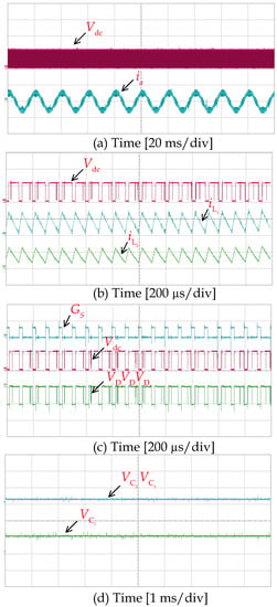
Figure 12.
Experimental results of the proposed S-qZSI: (a) DC-link voltage [100 V/div] and output phase-a current [2 A/div], (b) DC-link voltage [100 V/div] and inductor currents , [5 A/div], (c) gate signal [20 V/div], DC-link voltage [100 V/div] and diode voltages , , [100 V/div], and (d) capacitor voltages , , [100 V/div].
In summary, the simulations and experimental results have validated the superior performance of the S-qZSI in terms of high voltage gain, continuous input current, and low voltage stresses on the capacitors.
5. Conclusions
This paper has presented a modified switched quasi-Z-source inverter (S-qZSI) based on a switched-impedance network. In the proposed S-qZSI, the boost capability is enhanced by minor modifications compared with other switched-based Z-source networks. Moreover, the proposed S-qZSI features a continuous input current, which makes it suitable for renewable energy applications. In order to show the effectiveness of the proposed S-qZSI, a benchmarking with selected topologies was carried out. The comparison reveals that the voltage stresses of the inverter bridge power switches are lower than the other selected topologies, while the stress of the capacitor remains low. Therefore, the lower rating devices can be utilized to decrease the cost. Finally, the simulation and experimental results shows the superior performance in terms of high boost capability, lower voltage stresses of switches and capacitors, and continuous input currents.
Author Contributions
Conceptualization, J.Y., and Y.Y.; Formal analysis, J.Y.; Software, J.Y.; Validation, J.Y.; Writing—review and editing, J.Y., Y.Y., and F.B. All authors have read and agreed to the published version of the manuscript.
Funding
This research was funded by Reliable Power Electronic based Power Systems (REPEPS) by THE VELUX FOUNDATIONS (Award Ref. No.: 00016591).
Conflicts of Interest
The authors declare no conflict of interest.
References
- Peng, F.Z. Z-source inverter. IEEE Trans. Ind. Appl. 2003, 39, 504–510. [Google Scholar] [CrossRef]
- Yu, Y.; Zhang, Q.; Liang, B.; Liu, X.; Cui, S. Analysis of a single-phase Z-source inverter for battery discharging in vehicle to grid applications. Energies 2011, 4, 2224–2235. [Google Scholar] [CrossRef]
- Anderson, J.; Peng, F.Z. Four quasi-Z-Source inverters. In Proceedings of the 2008 IEEE Power Electronics Specialists Conference, Rhodes, Greece, 15–19 June 2008; pp. 2743–2749. [Google Scholar]
- Yuan, J.; Mostaan, A.; Yang, Y.; Siwakoti, Y.P.; Blaabjerg, F. A Modified Y-Source DC/DC Converter with High Voltage-Gains and Low Switch Stresses. IEEE Trans. Power Electron. 2020. [Google Scholar] [CrossRef]
- Mostaan, A.; Yuan, J.; Siwakoti, Y.P.; Esmaeili, S.; Blaabjerg, F. A Trans-Inverse Coupled-Inductor Semi-SEPIC DC/DC Converter With Full Control Range. IEEE Trans. Power Electron. 2019, 34, 10398–10402. [Google Scholar] [CrossRef]
- Serhii, S.; Husev, O.; Vinnikov, D.; Roncero-Clemente, C.; Pimentel, S.; Santasheva, E. Experimental Comparison of Two-Level Full-SiC and Three-Level Si–SiC Quasi-Z-Source Inverters for PV Applications. Energies 2019, 12, 2509. [Google Scholar]
- Honarmand, S.; Rajaei, A.; Shahparasti, M.; Luna, A.; Pouresmaeil, E. A Modified Partial Power structure for Quasi Z-Source Converter to Improve Voltage Gain and Power Rating. Energies 2019, 12, 2139. [Google Scholar] [CrossRef]
- Zhu, M.; Yu, K.; Luo, F.L. Switched Inductor Z-Source Inverter. IEEE Trans. Power Electron. 2010, 25, 2150–2158. [Google Scholar]
- Nguyen, M.; Lim, Y.; Cho, G. Switched-Inductor Quasi-Z-Source Inverter. IEEE Trans. Power Electron. 2011, 26, 3183–3191. [Google Scholar] [CrossRef]
- Li, D.; Loh, P.C.; Zhu, M.; Gao, F.; Blaabjerg, F. Generalized Multicell Switched-Inductor and Switched-Capacitor Z-Source Inverters. IEEE Trans. Power Electron. 2013, 28, 837–848. [Google Scholar] [CrossRef]
- Rostami, S.; Abbasi, V.; Kerekes, T. Switched capacitor based Z-source DC–DC converter. IET Power Electron. 2019, 12, 3582–3589. [Google Scholar] [CrossRef]
- Rostami, S.; Abbasi, V.; Blaabjerg, F. Implementation of a common grounded Z-source DC–DC converter with improved operation factors. IET Power Electron. 2019, 12, 2245–2255. [Google Scholar] [CrossRef]
- Ravindranath, A.; Mishra, S.K.; Joshi, A. Analysis and PWM Control of Switched Boost Inverter. IEEE Trans. Ind. Electron. 2013, 60, 5593–5602. [Google Scholar] [CrossRef]
- Nguyen, M.; Le, T.; Park, S.; Lim, Y. A Class of Quasi-Switched Boost Inverters. IEEE Trans. Ind. Electron. 2015, 62, 1526–1536. [Google Scholar] [CrossRef]
- Ho, A.; Chun, T.; Kim, H. Extended Boost Active-Switched-Capacitor/Switched-Inductor Quasi-Z-Source Inverters. IEEE Trans. Power Electron. 2015, 30, 5681–5690. [Google Scholar] [CrossRef]
- Nozadian, M.H.B.; Babaei, E.; Hosseini, S.H.; Asl, E.S. Steady-State Analysis and Design Considerations of High Voltage Gain Switched Z-Source Inverter with Continuous Input Current. IEEE Trans. Ind. Electron. 2017, 64, 5342–5350. [Google Scholar] [CrossRef]
- Ahmad, A.; Bussa, V.K.; Singh, R.K.; Mahanty, R. Switched-Boost-Modified Z-Source Inverter Topologies With Improved Voltage Gain Capability. IEEE J. Emerg. Sel. Top. Power Electron. 2018, 6, 2227–2244. [Google Scholar] [CrossRef]
- Liu, Y.; Abu-Rub, H.; Ge, B.; Blaabjerg, F.; Ellabban, O.; Loh, P.C. Impedance Source Power Electronic Converters; John Wiley & Sons: Hoboken, NJ, USA, 2016. [Google Scholar]


© 2020 by the authors. Licensee MDPI, Basel, Switzerland. This article is an open access article distributed under the terms and conditions of the Creative Commons Attribution (CC BY) license (http://creativecommons.org/licenses/by/4.0/).