Article

Numerical Study of 4H-SiC UMOSFETs with Split-Gate and P+ Shielding

1
Institute of Electronics Engineering, National Tsing Hua University, Hsinchu 30013, Taiwan
2
International College of Semiconductor Technology, National Chiao Tung University, Hsinchu 30010, Taiwan
3
School of Engineering and Computer Science, Washington State University, Vancouver, WA 98686, USA
*
Author to whom correspondence should be addressed.
Energies 2020, 13(5), 1122; https://doi.org/10.3390/en13051122
Submission received: 1 January 2020 / Revised: 25 February 2020 / Accepted: 26 February 2020 / Published: 2 March 2020
(This article belongs to the Special Issue Wide Bandgap Power Devices and Applications)

Abstract

:
In this paper, performances of a 4H-SiC UMOSFET with split gate and P+ shielding in different configurations are simulated and compared, with an emphasis on the switching characteristics and short circuit capability. A novel structure with the split gate in touch with the P+ shielding is proposed. The key design issues for 4H-SiC UMOSFETs are trench gate dielectric protection and reverse transfer capacitance Crss reduction. Based on simulation results, it is concluded that a UMOSFET with a gate structure combining split gate grounded to the trench bottom protection P+ shielding layer and a current spreading layer is achieved to yield the best compromise between conduction, switching, and short circuit performance. The split-gate design can effectively reduce Crss by shielding the coupling between the gate electrode and the drain region. The P+ shielding design not only protects the oxide at trench bottom corners but also minimizes the short channel effect due to drain-induced barrier lowing and the channel length modulation. Trade-off of the doping concentration of current spreading layer for UMOSFET is also discussed. A heavily doped current spreading layer may increase Crss and influence the switching time, even though RON,SP is reduced.

1. Introduction

SiC-based devices are promising candidates as power switches in various applications, thanks to the superior material properties of SiC, especially the wide bandgap, high critical electrical field, and excellent thermal conductivity [1]. Furthermore, gate dielectric of SiC devices can be formed by thermal oxidation with a good quality in a very similar way as in Si devices, which greatly facilitates the manufacturing of SiC devices. However, a high interface trap density (Dit) exists at the SiO2/SiC interface, which lowers the channel electron mobility and greatly increases RON,SP, particularly in the voltage range of 600–1700 V [2]. To reduce Dit in SiC MOSFETs, various gate oxide processes were developed, but the progress is still very limited as of today [3,4]. To circumvent the drawbacks brought by the low electron channel mobility, many approaches with different gate structures have also been proposed, and among them, the trench gate MOSFET (UMOSFET) is very promising. Unlike DMOSFETs, in which the cell density is limited by the horizontal JFET [5,6], UMOSFETs employ the very high cell density to minimize the contribution of channel resistance to the total on-state resistance. However, the electric field crowding at the trench gate bottom corner is a challenging issue in UMOSFETs [7,8], because the high critical electric field of 4H-SiC will bring a high electric field in the dielectrics and eventually cause long-term reliability concerns. One potential solution is to add a P+ shielding (PS) region at the bottom of the trench gate, so the electric field in the oxide at the trench gate corner can be reduced significantly [9,10]. However, such a design can introduce a parasitic JFET resistance along the current path and may require a current spreading layer to reduce it. Another important issue in the design of UMOSFETs is the large gate-to-drain capacitance (Cgd) which comes from the large cell density. Cgd plays an important role in MOSFETs since it corresponds to the reverse transfer capacitance Crss, which is related to dV/dt during hard switching and affects switching performance [11]. In a conventional gate structure of UMOSFETs, Cgd is large due to a large gate electrode area coupled with the N-drift region through trench bottom oxide. With a thick bottom oxide, this issue can be alleviated. The PS and split-gate (SG) structures in UMOSFET are shown to solve this problem even more effectively [12,13]. Cgd can be reduced by simply grounding SG or PS to the source electrode. Besides switching performance, another important characteristic of power-switching devices is the short-circuit capability, particularly in motor-drive applications. In short-circuit conditions, the current of a power device should be limited to prevent the device from experiencing thermal destruction and prolong its short-circuit withstand time. This paper is an extended study of a previous report [14], but it proposes a new gate structure of a SG under the control gate and in contact with the PS. All the critical issues associated with different gate structures are investigated and compared in this paper. Moreover, the short-circuit capability of SiC UMOSFETs affected by drain-induced barrier lowing (DIBL) is also explored for the first time. Finally, a new design is suggested, which can not only retain the advantages of conventional UMOSFETs such as low RON,SP and high blocking voltage, but also minimize the electric field in the oxide at the trench gate corner and possess a superior short-circuit capability.

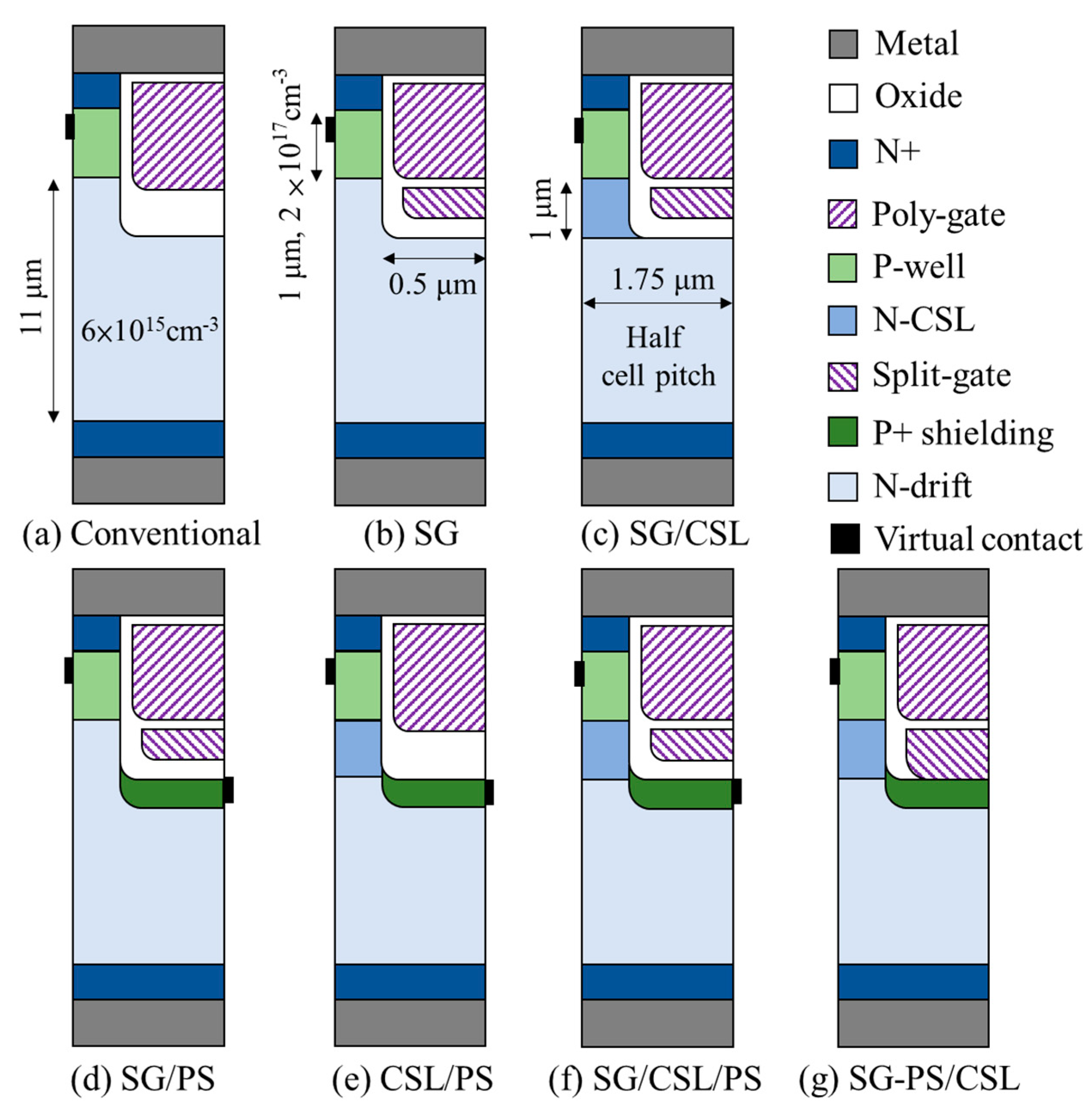
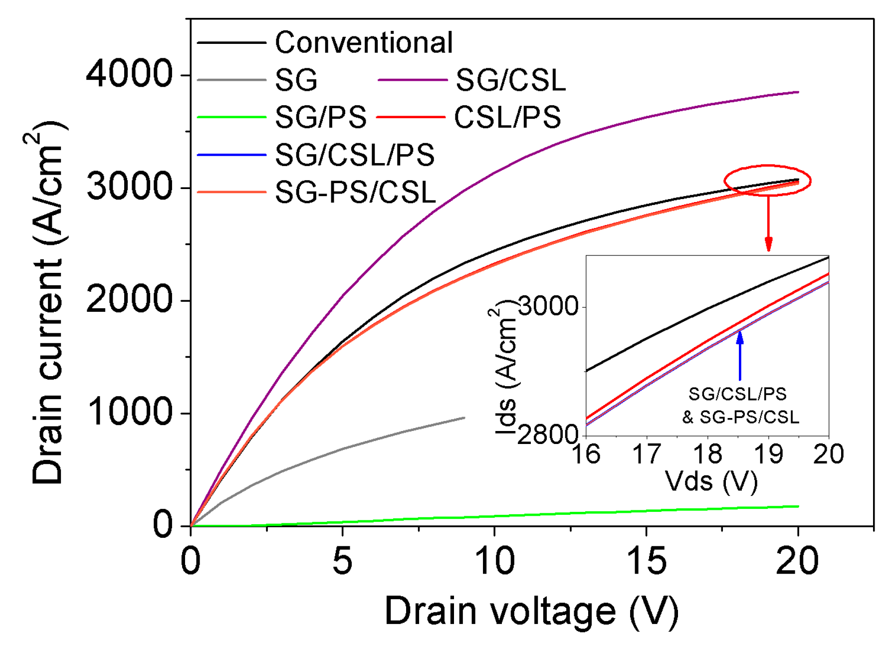
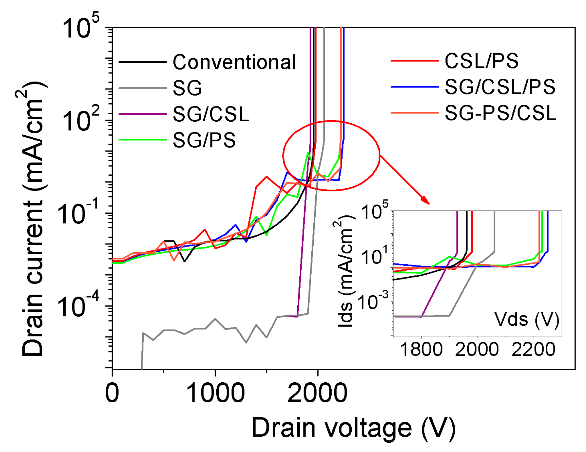
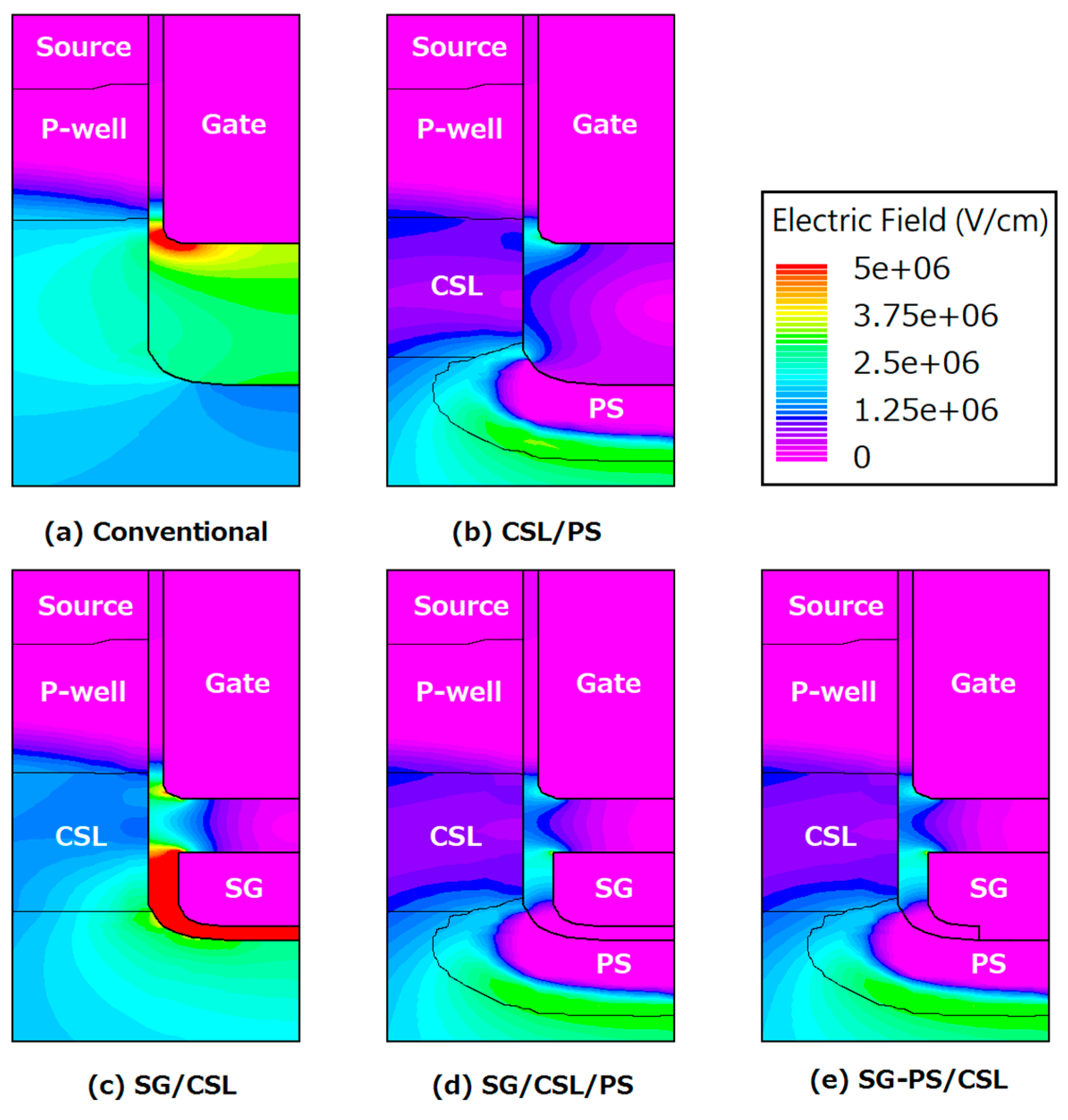
2. DC and Reverse Characteristics

Figure 1 is a summary of the gate structures simulated in this paper. Figure 1a shows a conventional gate structure of UMOSFET with a thick bottom oxide. In Figure 1b, a SG is inserted underneath the control gate. In Figure 1c, an N-type current spreading layer (CSL) is inserted between the N-drift layer and p-well layer. In Figure 1d, a heavily doped P-type layer created by ion implantation, i.e., the PS region, is placed underneath the trench gate of Figure 1b. In this case, CSL is not included. Figure 1e includes CSL and PS but without SG. Figure 1f shows a trench gate structure merging CSL, PS, and SG. At last, a novel structure with SG in direct contact to PS (SG–PS/CSL) is proposed as shown in Figure 1g. In all of the gate structures revealed above, SG and PS are both shorted to the source electrode hypothetically. In real device design and operation, PS needs a low resistive path to the source electrode, to minimize possible RC time delay during device switching, which is difficult to achieve in the device layout, since P-type 4H-SiC is resistive. This difficulty is usually overcome by complicated gate structures with some sacrifices of the device performance [10]. By simply removing the oxide between SG and PS, as shown in Figure 1g, PS can be shorted to source electrode through SG which is usually heavily doped and therefore highly conductive. In this case, SG has to be p-type doped to avoid a pn junction at the SG/PS interface. Although not shown in the two-dimensional schematics in Figure 1, the P-wells and PS of all these devices are assumed shorted to the source electrode through n+ source openings and other locations in the third dimension. In simulation, this is done with virtual contacts connected to the source electrode at appropriate locations on the symmetry plane, as depicted in Figure 1.
All of the aforementioned structures are designed for 1200 V applications, with an 11 μm thick and 6 × 1015 cm−3 doped drift layer. The gate width is assumed to be 1 μm, which is practical for current 6-inch and 8-inch foundry technologies. In order to take advantage of UMOSFETs for high cell density, the cell pitch is fixed to be 3.5 μm, which is smaller than state-of-the-art 4H-SiC DMOSFETs. CSL in the baseline structure has a thickness of 1 μm and N-type doping concentration of 9 × 1016 cm−3. The P-well is assumed to be epitaxially grown on top of the drift layer, with a 1 μm thickness and 2 × 1017 cm−3 doping concentration, followed by an epitaxial N+ source region of 0.5 μm in thickness and uniform 1 × 1020 cm−3 in concentration. The channel length of all UMOSFETs in Figure 1 is kept at 1 μm. The PS region is formed by ion implantation with the peak concentration of 1 × 1020 cm−3, the dose of 3.2 × 10¹⁵ /cm2, and the maximum energy of 180 keV. All the simulation parameters are default in Silvaco, except that the channel electron mobility is adjusted to be around 20 cm2/Vs, corresponding to the present status of SiO2/4H-SiC by nitridation treatment. The extracted threshold voltage is 6.5 V from Id-Vg curves. The gate trench is over-etched through the P-well to a depth of 1.2 μm. The SG region is assumed to be 0.5 μm thick. For SG–PS/CSL, the SG is assumed p-type, while for other structures, it is assumed n-type as the control gate. The simulations are carried out using Silvaco.
Figure 2 summarizes the simulated on-state characteristics of the SiC UMOSFET structures at room temperature. As can be observed, both structures without CSL exhibit much higher on-state resistances than that of the conventional structure, indicating that, in fine cell pitch structures, current spreading is important, especially when there is a parasitic JFET effect by PS and P-well. The specific on-resistance of the SG/CSL/PS structure and the proposed SG–PS/CSL structure is 2.33 mΩ-cm2 at Vgs = 20 V, comparable to that of the conventional structure. For SG/CSL, the specific on-resistance can be further reduced to 2.00 mΩ-cm2 since therefore is no PS and therefore no JFET effect. However, this structure suffers from other effects, as shown in the next discussion.
The room-temperature reverse characteristics of the above structures are simulated and displayed in Figure 3. They all satisfy the required 1200 V rated blocking voltage with sufficient margin. In real devices, the reverse blocking capability is mostly limited by the edge termination, but this is not the focus of this study. The largest breakdown voltage in cell structure by simulation is 2250 V achieved by SG/PS, SG–PS/CSL, and SG/CSL/PS structures. The insertion of CSL will not affect the static blocking capability if properly designed. Another critical issue to be considered is the electric field in the gate oxide, especially at the trench gate bottom corner. Such high electric field is detrimental to device reliability, as pointed out in previous reports [15,16]. Figure 4 depicts the electric field distribution in the gate oxide near the trench bottom of conventional, SG/CSL, CSL/PS, and SG/CSL/PS structures, all at a drain voltage of 1600 V in the off state and without severe RON,SP degradation. As can be observed in Figure 4, without PS underneath the trench bottom, high electric field exceeding 5 MV/cm appears in the oxide of the conventional and SG/CSL structures, even with a thick bottom oxide of 0.1 μm and rounded trench bottom corners, causing Vth and Id,lin degradation after long-term reverse stress. On the other hand, the maximum electric field is always in the semiconductor in CSL/PS and SG/CSL/PS structures under the same bias condition, while the electric field in gate oxide is well below 3 MV/cm. In this case, stable and reliable reverse operation can be expected. It is worth noting that the electric field in the oxide in SG–PS/CSL is basically identical to the oxide in SG/CSL/PS.

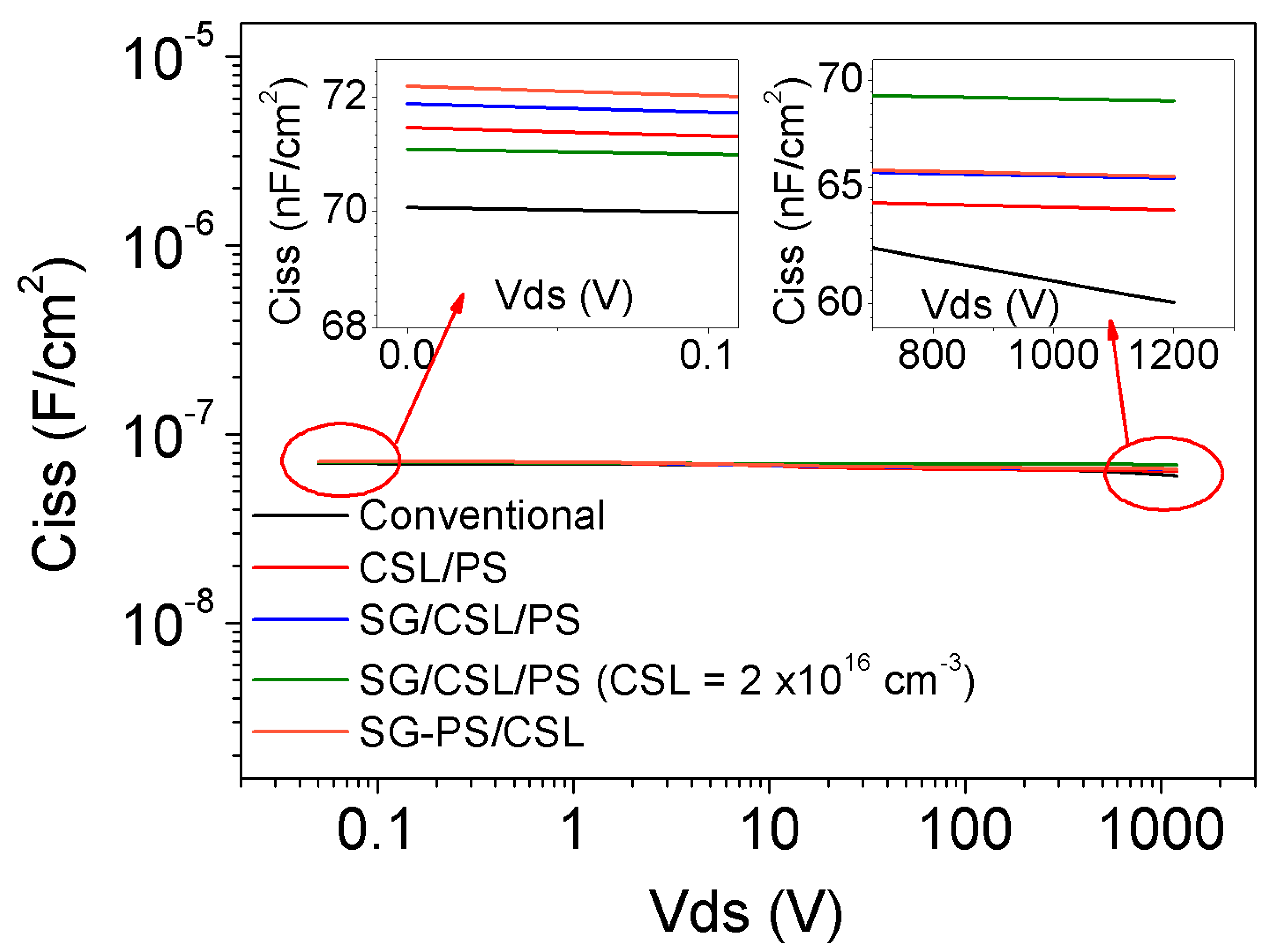
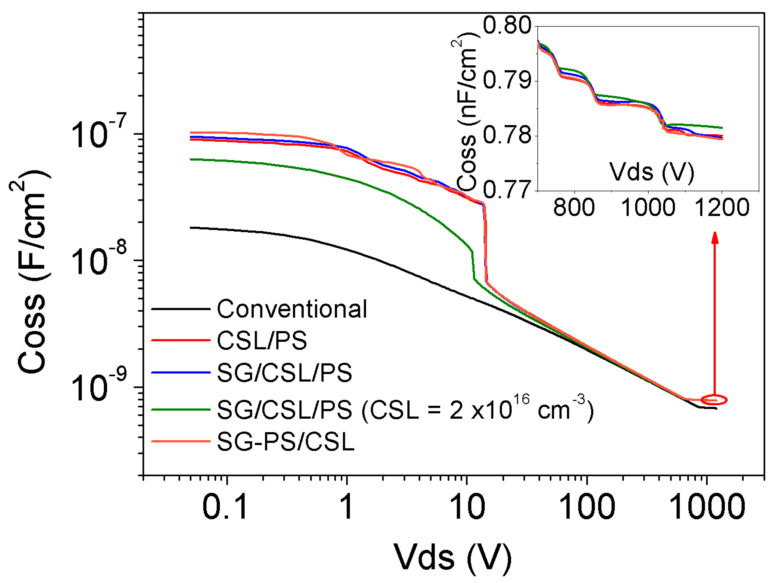
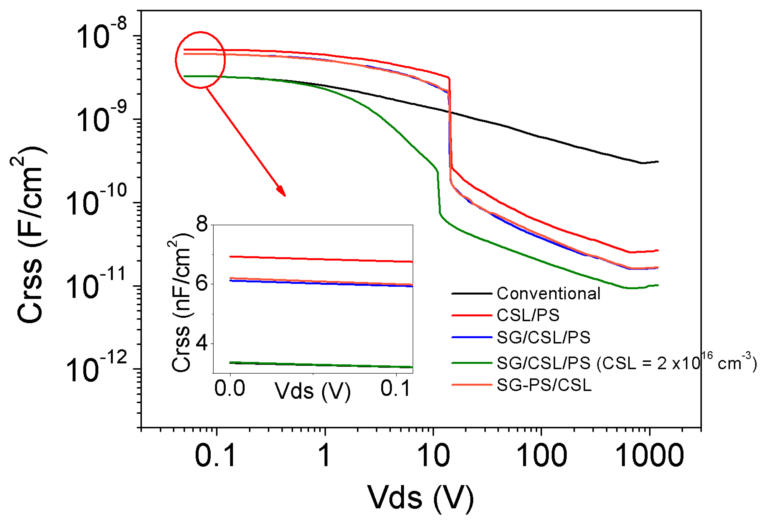
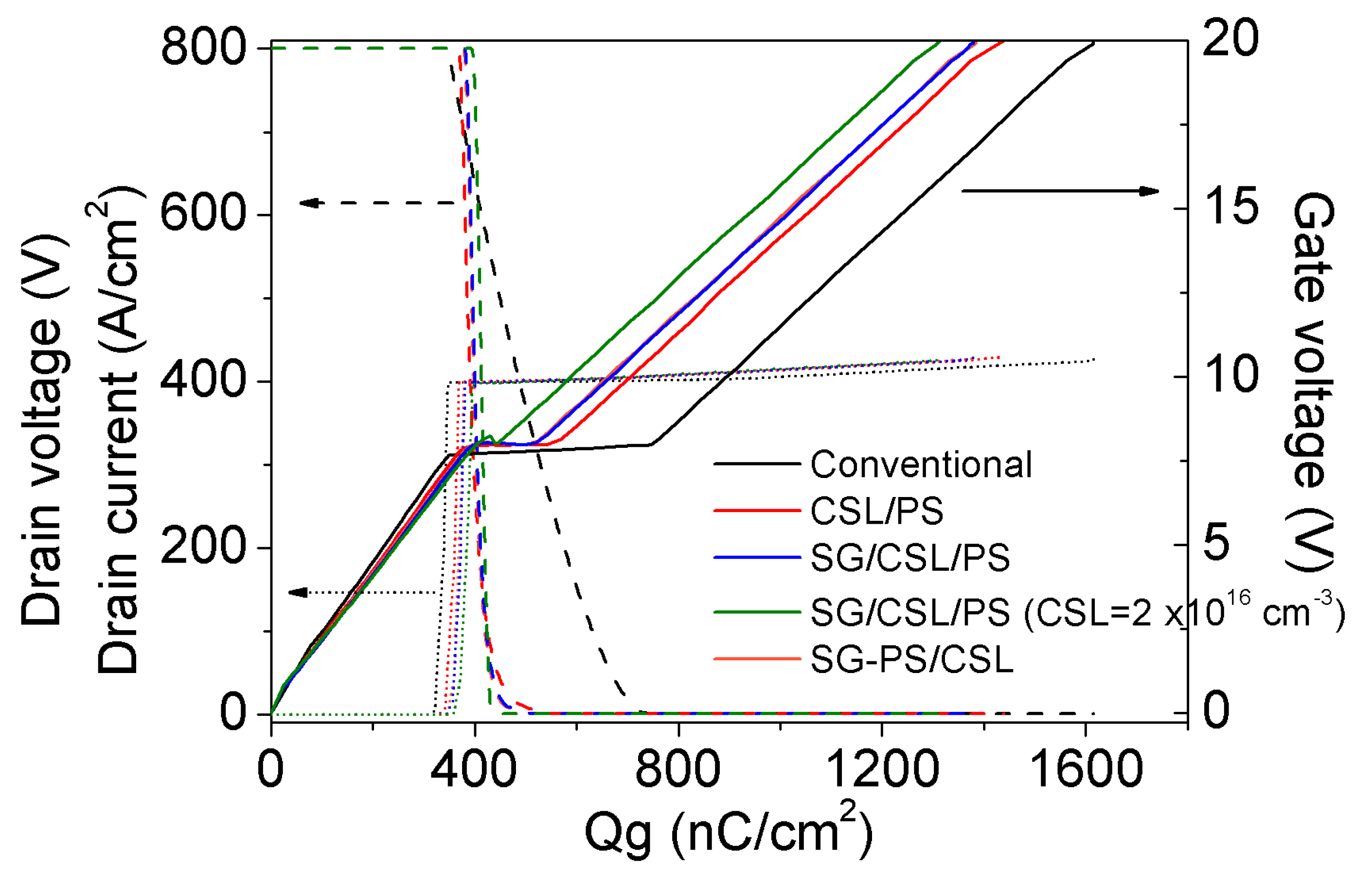
3. AC and Switching Characteristics

AC and switching performances are further investigated, with a focus on the most promising CSL/PS, SG/CSL/PS, and SG–PS/CSL structures in comparison with the conventional structure. Figure 5 shows the simulated Ciss versus Vds curves at the frequency of 1 MHz and biased at Vgs = 0 V. As in typical MOSFET structures, Ciss is mostly coming from Cgs and has a very weak dependence on Vds. Since there is no contribution from the capacitance between the control gate and SG which is grounded to source, or the capacitance between the control gate and PS, which is also grounded to source, Ciss of the conventional gate structure is the lowest. Luckily Ciss of other gate structures are not much larger either, since those capacitances are reduced by increasing the oxide thickness at the proper locations, for example, between the control gate and SG. Figure 6 summarizes Coss, with two main features observed. First, at a low Vds (< 10 V), Coss of the conventional structure is much lower than that of CSL/PS and SG/CSL/PS. This is attributed to the narrow depletion region of the PN junction due to the high doping concentration of CSL, which increases Csd and Cgd. Second, a distinct drop exists in Coss curves of CSL/PS and SG/CSL/PS but not the conventional gate structure. Such drop is a unique feature of superjunction or superjunction-like devices, and is attributed to the pinch-off of CSL at a high reverse bias, which is similar to the n-pillars in silicon superjunction MOSFETs. In the case of 4H-SiC split-gate UMOSFETs, in addition to the vertical depletion from the P-well, lateral depletion coming from SG or PS will fully deplete CSL at a pinch-off voltage and dramatically reduce Csd and Cgd. It is also clear that, with a lightly doped CSL of 2 × 1016 cm−3, the pinch-off occurs at a smaller Vds. To further elaborate on this, Crss (= Cgd) of conventional, CSL/PS, and SG/CSL/PS structures with different CSL doping concentrations are summarized in Figure 7, with the drop clearly demonstrated. Before pinch-off, the depletion capacitance in CSL contributes a significant amount to Cgd when the doping concentration is high in the case of 9 × 1016 cm−3, and therefore Crss is larger in CSL/PS and SG/CSL/PS than in the conventional. However, when the CSL concentration is low in the case of 2 × 1016 cm−3, the depletion capacitance is small enough, and Crss becomes very close to the value of the conventional structure. After pinch-off, because of the shielding from SG and PS underneath the control gate, Crss in CSL/PS and SG/CSL/PS is significantly reduced when compared to that in the conventional structure. The fact that CSL is more easily depleted with a lower concentration and the benefit of SG is also reflected by Crss values.
Figure 8 summarizes the gate-charge waveforms of the five gate structures in Figure 5, under clamped inductive load-switching tests at 800 V bias. The relationship between Qgd and Crss (Cgd) can be described as Equation (1) [17]:
Qgd = V o n V D D Cgd ( Vds ) d Vds
where Qgd is the gate charge in the gate plateau region (around Vgs = 7.5 V) and VDD = 800 V in Figure 8. From Figure 7, it is obvious that the Crss is larger for the conventional structure for most of the Vds range and is smaller for the split-gate structure. As expected from Equation (1), Qgd of SG/CSL/PS is much lower than that of conventional, and is further reduced when the doping concentration of CSL decreases. From the above simulation results, it is worth mentioning that the DC and AC performance of SG–PS/CSL is almost identical to that of SG/CSL/PS, which is reasonable since the main features of the two structures are very similar. It should be noted that in real applications parasitic inductances in such high dV/dt must be considered since they might induce a large voltage overshoot in the switching waveforms and raise EMI and reliability concerns [18]. Active gate drivers are required to achieve the best switching performance while overcoming these drawbacks, which is beyond the scope of this paper.

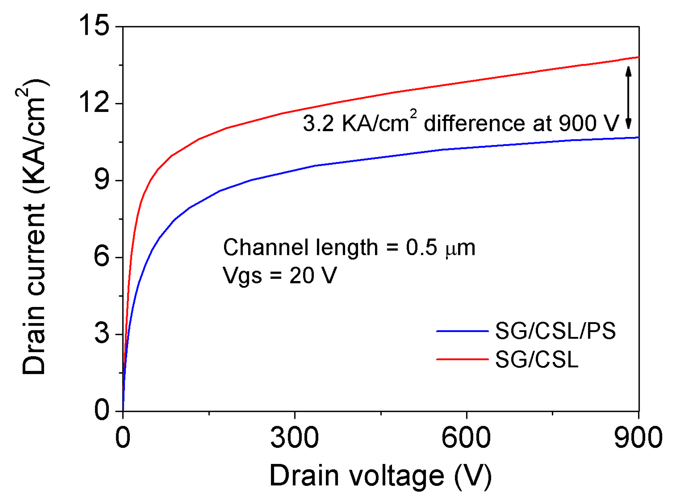
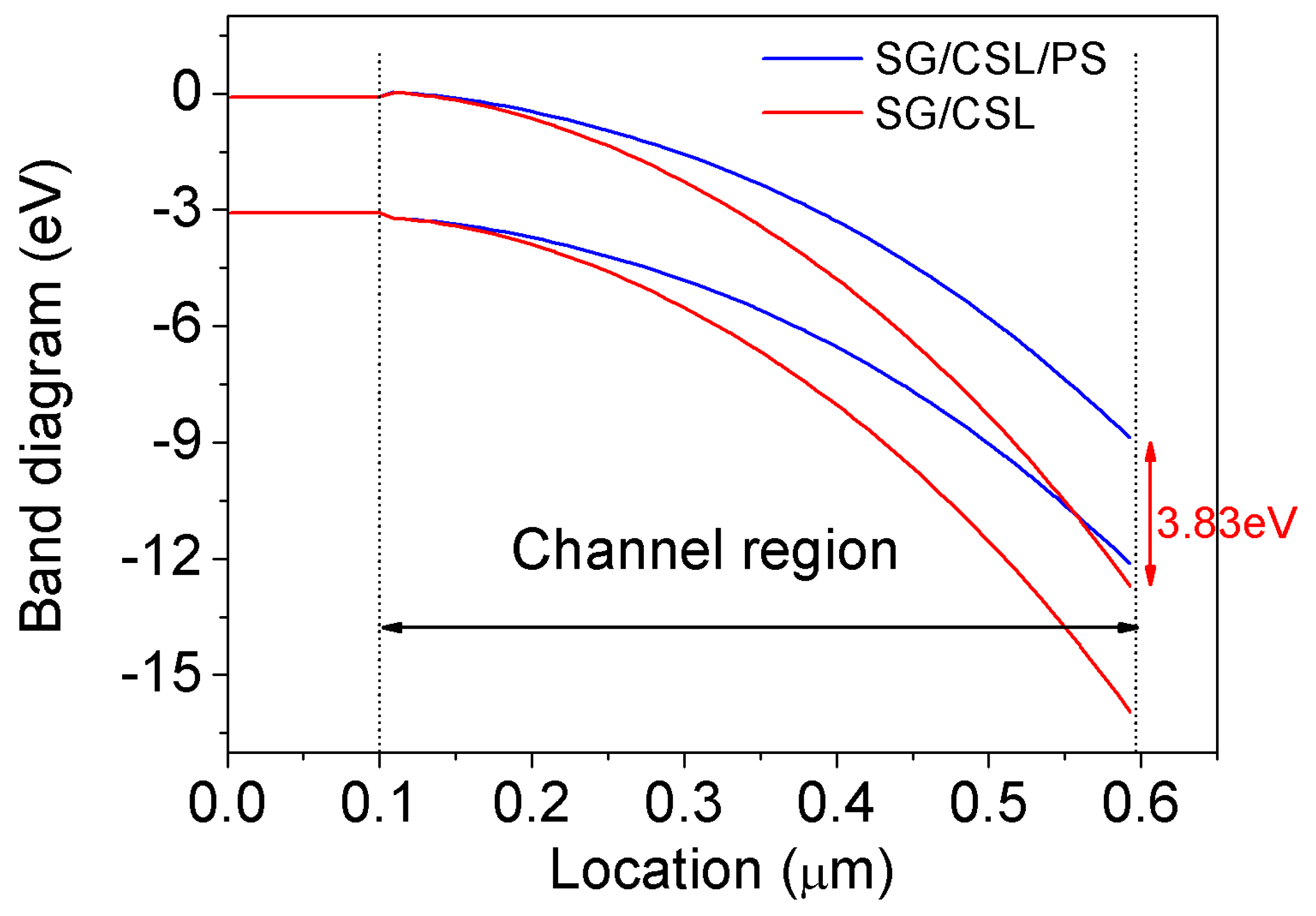
4. Short-Circuit Capability

The short-circuit capability of power-switching devices is of great importance, particularly for motor-drive applications. In this section, we discuss the importance of the PS region to the short-circuit capability of 4H-SiC UMOSFETs. A common approach to reduce channel resistance in 4H-SiC MOSFETs is to use submicron channel length, where short channel effects are inevitable [19,20]. In Figure 9, simulated Id-Vds curves in the saturation region of SG/CSL and SG/CSL/PS are compared. A channel length of 0.5 μm is used. It is clear that the insertion of PS can reduce the saturation current in the high Vds regime and therefore improve the short-circuit capability, which is limited by thermal constrains [21,22]. A band diagram along the vertical channel is plotted in Figure 10, when Vgs is 20 V and Vds is 900 V. With the PS region, the channel is shielded from the drain potential, even at such high drain bias, and therefore the channel length modulation, as well as the drain-induced barrier lowering (DIBL) effect in the device is relieved This reduces the saturation current and power dissipation during short-circuit duration, similar to what has been reported for silicon IGBT [23,24].
The key performance indexes of the potential gate structures investigated in this study are listed in Table 1. It is shown that a trench gate structure with SG/CSL/PS or SG–PS/CSL implemented can achieve very good DC and AC performance compared to conventional structure without suffering from high electric field in the gate oxide.

5. Conclusions

In this paper, different gate structures in 4H-SiC UMOSFETs are numerically studied with focus on their DC, AC, and short-circuit performances. From the simulation results, trench gate structure with SG/CSL/PS or SG–PS/CSL show better DC and AC performance without suffering from high electric field in the gate oxide or high specific on-resistance. In addition, with the P+ shielding underneath the trench gate, the channel length is allowed to shrink without the risk of poor short-circuit capability, owing to high saturation current from the channel length modulation and drain-induced barrier-lowering effect.

Author Contributions

Conceptualization, J.-Y.J. and C.-F.H.; formal analysis, J.-Y.J.; methodology, J.-Y.J. and C.-F.H.; validation, T.-L.W. and F.Z.; writing—original draft, J.-Y.J., F.Z. and C.-F.H.; writing—review and editing, T.-L.W. All authors have read and agreed to the published version of the manuscript.

Funding

This research is financially sponsored in part by MOST through project no. 107-2218-E-007-042 and 107-2923-E-007-008-MY2, as well as the WSU Vancouver External Mentoring Program.

Acknowledgments

The authors would like to thank Taiwan Semiconductor Research Institute for their support in device simulations. F. Zhao and C. F. Huang thank the WSU Vancouver External Mentoring Program for its support of this work.

Conflicts of Interest

The authors declare no conflict of interest.

References

  1. Kimoto, T.; Cooper, J.A. Fundamentals of Silicon Carbide Technology: Growth, Characterization, Devices and Applications; John Wiley & Sons: Hoboken, NJ, USA, 2014. [Google Scholar]
  2. Cheng, L.; Agarwal, A.K.; Dhar, S.; Ryu, S.; Palmour, J.W. Static performance of 20 A, 1200 V 4H-SiC power MOSFETs at temperatures of −187 °C to 300 °C. J. Electron. Mater. 2012, 41, 910–914. [Google Scholar] [CrossRef]
  3. Yano, H.; Hatayama, T.; Fuyuki, T. POCl3 annealing as a new method for improving 4H-SiC MOS device performance. ECS Trans. 2013, 50, 257–265. [Google Scholar] [CrossRef]
  4. Nanen, Y.; Kato, M.; Suda, J.; Kimoto, T. Effects of nitridation on 4H-SiC MOSFETs fabricated on various crystal faces. IEEE Trans. Electron Devices 2013, 60, 1260–1262. [Google Scholar] [CrossRef]
  5. Ryu, S.; Krishnaswami, S.; O’Loughlin, M.; Richmond, J.; Agarwal, A.; Palmour, J.; Hefner, A.R. 10-kV, 123-mΩ∙cm2 4H-SiC Power DMOSFETs. IEEE Electron Device Lett. 2004, 25, 556–558. [Google Scholar] [CrossRef]
  6. Saha, A.; Cooper, J.A. A 1-kV 4H-SiC power DMOSFET optimized for low on-resistance. IEEE Trans. Electron Devices 2007, 54, 2786–2791. [Google Scholar] [CrossRef]
  7. Nakamura, T.; Nakano, Y.; Aketa, M.; Nakamura, R.; Mitani, S.; Sakairi, H.; Yokotsuji, Y. High performance SiC trench devices with ultra-low Ron. In Proceedings of the 2011 International Electron Devices Meeting, Washington, DC, USA, 5–7 December 2011. [Google Scholar]
  8. Rashid, S.J.; Mihaila, A.; Udrea, F.; Amaratunga, G. Trench oxide protection for 10 kV 4H-SiC trench MOSFETs. In Proceedings of the Fifth International Conference on Power Electronics and Drive Systems, Singapore, 17–20 November 2003. [Google Scholar]
  9. Li, Y.; Cooper, J.A.; Capano, M.A. High-Voltage (3 kV) UMOSFETs in 4H-SiC. IEEE Trans. Electron Devices 2002, 49, 972–975. [Google Scholar] [CrossRef]
  10. Peters, D.; Siemieniec, R.; Aichinger, T.; Basler, T.; Esteve, R.; Bergner, W.; Kueck, D. Performance and ruggedness of 1200V SiC-Trench-MOSFET. In Proceedings of the 2017 29th International Symposium on Power Semiconductor Devices and IC’s (ISPSD), Sapporo, Japan, 28 May–1 June 2017. [Google Scholar]
  11. Barkhordarian, V. Application Note AN-1084, Infineon/IR. Available online: https://www.infineon.com/dgdl/an-1084.pdf?fileId=5546d462533600a401535595840d101e (accessed on 24 December 2019).
  12. Ebihara, Y.; Ichimura, A.; Mitani, S.; Noborio, M.; Takeuchi, Y.; Mizuno, S.; Yamamoto, T.; Tsuruta, K. Deep-P encapsulated 4H-SiC trench MOSFETs with ultra low RonQgd. In Proceedings of the 2018 IEEE 30th International Symposium on Power Semiconductor Devices and ICs (ISPSD), Chicago, IL, USA, 13–17 May 2018. [Google Scholar]
  13. Wei, J.; Zhang, M.; Jiang, H.; Wang, H.; Chen, K.J. Dynamic degradation in SiC trench MOSFET with a floating p-shield revealed with numerical simulations. IEEE Trans. Electron. Devices 2017, 64, 2592–2598. [Google Scholar] [CrossRef]
  14. Jiang, J.-Y.; Huang, C.-F.; Wu, T.-L.; Zhao, F. Simulation Study of 4H-SiC Trench MOSFETs with Various Gate Structures. In Proceedings of the Electron Devices Technology and Manufacturing Conference (EDTM), Singapore, 12–15 March 2019. [Google Scholar]
  15. Agarwal, A.K.; Siergiej, R.R.; Seshadri, S.; White, M.H.; McMullin, P.G.; Burk, A.A.; Rowland, L.B.; Brandt, C.D.; Hopkins, R.H. A critical look at the performance advantages and limitations of 4H-SiC power UMOSFET structures. In Proceedings of the 8th International Symposium on Power Semiconductor Devices and ICs, Maui, HI, USA, 23 May 1996. [Google Scholar]
  16. Tanaka, R.; Kagawa, Y.; Fujiwara, N.; Sugawara, K.; Fukui, Y.; Miura, N.; Imaizumi, M.; Yamakawa, S. Impact of grounding the bottom oxide protection layer on the short-circuit ruggedness of 4H-SiC trench MOSFETs. In Proceedings of the 2014 IEEE 26th International Symposium on Power Semiconductor Devices & IC’s (ISPSD), Waikoloa, HI, USA, 15–19 June 2014. [Google Scholar]
  17. Baliga, B.J. Fundamentals of Power Semiconductor Devices; Springer: Berlin/Heidelberg, Germany, 2008. [Google Scholar]
  18. Idir, N.; Bausiere, R.; Franchaud, J.J. Active gate voltage control of turn-on di/dt and turn-off dv/dt in insulated gate transistors. IEEE Trans. Power Electron. 2006, 21, 849–855. [Google Scholar] [CrossRef]
  19. Matin, M.; Saha, A.; Cooper, J.A. A self-aligned process for high-voltage, short-channel vertical DMOSFETs in 4H-SiC. IEEE Trans. Electron Devices 2004, 51, 1721–1725. [Google Scholar] [CrossRef]
  20. Noborio, M.; Kanzaki, Y.; Suda, J.; Kimoto, T. Experimental and theoretical investigations on short-channel effects in 4H-SiC MOSFETs. IEEE Trans. Electron Devices 2005, 52, 1954–1962. [Google Scholar] [CrossRef] [Green Version]
  21. Otsuki, M.; Onozawa, Y.; Kanemaru, H.; Seki, Y.; Matsumoto, T. A study on the short-circuit capability of field-stop IGBTs. IEEE Trans. Electron Devices 2003, 50, 1525–1531. [Google Scholar] [CrossRef]
  22. Knoll, L.; Mihaila, A.; Kranz, L.; Bellini, M.; Wirths, S.; Bianda, E.; Papadopoulos, C.; Rahimo, M. Dynamic switching and short circuit capability of 6.5kV silicon carbide MOSFETs. In Proceedings of the 2018 IEEE 30th International Symposium on Power Semiconductor Devices and ICs (ISPSD), Chicago, IL, USA, 13–17 May 2018. [Google Scholar]
  23. Eikyu, K.; Sakai, A.; Matsuura, H.; Nakazawa, Y.; Akiyama, Y.; Yamaguchi, Y.; Inuishi, M. On the scaling limit of the Si-IGBTs with very narrow mesa structure. In Proceedings of the 2016 28th International Symposium on Power Semiconductor Devices and ICs (ISPSD), Prague, Czech, 12–16 June 2016. [Google Scholar]
  24. Tanaka, M.; Nakagawa, A. Conductivity modulation in the channel inversion layer of very narrow mesa IGBT. In Proceedings of the 2017 29th International Symposium on Power Semiconductor Devices and IC’s (ISPSD), Sapporo, Japan, 28 May–1 June 2017. [Google Scholar]
Figure 1. Schematics of different gate structures studied in this paper. A novel proposed UMOSFET with SG in contact with PS structure is shown in (g). All devices have a cell pitch of 3.5 μm. (a). Conventional; (b). SG; (c). SG/CSL; (d). SG/PS; (e). CSL/PS; (f). SG/CSL/PS; (g). SG-PS/CSL.
Energies 13 01122 g001
Figure 2. The on-state characteristics of different gate designs at Vgs = 20 V. The RON,SP of the proposed SG/CSL/PS structure is 2.33 mΩ-cm2. © (2020) IEEE. Reproduced, with permission, from [14].
Energies 13 01122 g002
Figure 3. The reverse blocking characteristics between different gate designs. The breakdown voltages of the proposed SG–PS/CSL and SG/CSL/PS structure is 2250 V. © (2020) IEEE. Reproduced, with permission, from [14].
Energies 13 01122 g003
Figure 4. The electrical field distribution in different gate designs at Vds = 1600 V. The devices without PS (a,c) show a relative high electric field at the gate trench bottom corner. In simulation, P-well and SG are connected to the source electrode through virtual contacts at locations indicated in Figure 1. (a). Conventional; (b). CSL/PS; (c). SG/CSL; (d). SG/CSL/PS; (e). SG-PS/CSL.
Energies 13 01122 g004
Figure 5. Ciss of conventional, CSL/PS, SG–PS/CSL, and SG/CSL/PS, with different CSL doping concentrations. The frequency is at 1 MHz and Vgs is 0 V. If not otherwise specified, the CSL doping concentration is 9 × 1016 cm−3.
Energies 13 01122 g005
Figure 6. Coss of conventional, CSL/PS, SG–PS/CSL, and SG/CSL/PS, with different CSL doping concentrations. The frequency is at 1 MHz and Vgs is 0 V. If not otherwise specified, the CSL doping concentration is 9 × 1016 cm−3.
Energies 13 01122 g006
Figure 7. Crss of conventional, CSL/PS, SG–PS/CSL, and SG/CSL/PS, with different CSL doping concentrations. The frequency is at 1 MHz and Vgs is 0 V. If not otherwise specified, the CSL doping concentration is 9 × 1016 cm−3. © (2020) IEEE. Reproduced, with permission, from [14].
Energies 13 01122 g007
Figure 8. Gate-charge waveforms of conventional, CSL/PS, SG–PS/CSL, and SG/CSL/PS, under 800 V clamped inductive load switching. If not otherwise specified, the CSL doping concentration is 9 × 1016 cm−3. © (2020) IEEE. Reproduced, with permission, from [14].
Energies 13 01122 g008
Figure 9. Id-Vds curves in the saturation region of SG/CSL and SG/CSL/PS.
Energies 13 01122 g009
Figure 10. Energy band diagram of SG/CSL and SG/CSL/PS when Vgs = 20 V and Vds = 900 V.
Energies 13 01122 g010
Table 1. Key performance indexes of the gate structures studied in this paper.
CharacteristicsUnitConventionalCSL/PS
CSL = 9 × 1016 cm−3
SG/CSL/PS
CSL = 9 × 1016 cm−3
SG/CSL/PS
CSL = 2 × 1016 cm−3
SG–PS/CSL
CSL = 9 × 1016 cm−3
RON,SPmΩcm22.382.322.332.602.33
Maximum Eox at 1600 VMV/cm7.52.12.21.22.2
QgsnC/cm2339360374436371
QgdnC/cm240820914929149
Ciss at 800 VnF/cm261.8664.2665.6369.2165.72
Coss at 800 VpF/cm2714790791792790
Crss at 800 VpF/cm22992516916
RON x QGDmΩnC97148534775347

