Abstract
This work describes an efficient implementation in terms of computation time and resource usage in a Field-Programmable System-On-Chip (FPSoC) of a Finite Control Set Model Predictive Control (FCS-MPC) algorithm. As an example, the FCS-MPC implementation is used for the current reference tracking of a two-level three-phase power converter. The proposed solution is an enabler for using both complex control algorithms and digital controllers for high switching frequency semiconductor technologies. An original HW/SW (hardware and software) system architecture for an FPSoC is designed to take advantage of a modern operating system, while removing time uncertainty in real-time software tasks, and exploiting dedicated FPGA fabric for the most complex computations. In addition, two different architectures for the FPGA-implemented functionality are proposed and compared in order to study the area-speed trade-off. Experimental results show the feasibility of the proposed implementation, which achieves a speed hundreds of times faster than the conventional Digital Signal Processor (DSP)-based control platform.
1. Introduction
Voltage source inverters (VSI) are an industry standard for power conversion, and are extensively applied in different fields such as renewable energy integration, motor drives, or energy storage [1,2,3,4]. The general trend for these applications is the search for new and more ambitious control methods, and the use of new devices that allow higher switching frequencies with reduced power losses. Nonetheless, these improvements usually translate into a greater computational demand on control platforms.
Among all the types of control schemes proposed for these converters, Finite Control Set Model Predictive Control (FCS-MPC) has been developed in previous research [5,6,7,8], leading to an improved dynamic response and the capability to achieve simultaneous control targets. This result has led to growing attention for this type of control in the field of power electronics [9,10,11].
One of the main challenges hindering the penetration of these control strategies in the industry is indeed the great computational burden that they represent for most conventional digital platforms [12]. When it comes to digital control platforms, Microprocessors and Digital Signal Processing (DSPs) systems have become the standard in the field of power electronics [13]. This is due to their low cost, low consumption, well-known programming methods, and the presence of many dedicated peripherals that offer specialized and integrated solutions for the usual power electronics applications [14]. Nonetheless, the need for ever-increasing performance of digital systems calls for the exploration of new digital platforms that are capable of facing the high computational complexity of new control algorithms like FCS-MPC [12,15].
In addition to this, the introduction of wide band-gap semiconductors based on materials like Silicon Carbide (SiC) or Gallium Nitride (GaN) is allowing the development of power electronics applications with much higher switching frequencies (in the range of hundreds of kilohertz) [16], in comparison to conventional silicon-based semiconductors. This allows the arrival of new, high-performance power converters with reduced size that are capable of achieving very high quality output voltages and currents. These characteristics represent great advantages for many industries like aeronautics [17,18]. Nonetheless, they represent an important challenge for any control platform that would need to perform the required calculations in a much shorter period of time [19,20].
Field-Programmable Gate Array (FPGA) devices are becoming considered in state-of-the-art applications in the field of power electronics [21]. Works with FPGA-based control have been published through the years [15,22,23,24]. In these designs, FPGAs are usually used as external peripherals that generate the switching signals for the converter or help the DSP with some calculations. Beyond these research efforts, DSP and microcontrollers are still the main players in power electronics applications.
Some of the main difficulties when it comes to the growth of FPGA-based control architectures in this field are the proficiency requirement for designers in hardware description languages (HDL) and the need to establish a communication channel between the FPGA and the rest of the digital hardware [25]. To solve these issues, the arrival of new technologies like High-Level-Synthesis (HLS) tools that allow the compilation of high level programming languages into HDL have made FPGA devices a more accessible solution for designers [26,27]. Allowing working at a higher level of abstraction, HLS has also helped to greatly reduce the required time-to-market of these solutions, at the expense of increasing the area consumption compared to HDL designs [28,29,30,31].
In addition to this, the arrival of FPSoC platforms that combine the calculation power of FPGA fabric with the high-level solutions of hard processing systems are greatly helping the introduction of these digital platforms in power electronics applications [28,32]. These platforms offer a wide range of powerful resources combined with the advantages of System-on-Chip platforms such as reduced size and consumption and better reliability and performance. The availability of all these resources in a single chip presents great opportunities to reduce the execution times of control algorithms by parallelizing tasks and using the programmable logic to accelerate calculations. Also, the usual bottleneck that would appear in the digital communication of these components is reduced due to the availability of low latency interface solutions in a SoC. These features make FPSoCs promising platforms for the control implementation of applications in the field of power electronics, especially with the arrival of the aforementioned high switching frequency semiconductor technologies based on Wide Band-gap materials. However, designing for these platforms compounds the complexity of FPGA technology with the intricacies of multiprocessor parallel programming and the design of efficient HW/SW interfaces to transfer data.
In this paper, the implementation of an FCS-MPC algorithm for an FPSoC is carried out. In particular, this work is implemented in a Xilinx Zynq 7000 FPSoC [33]. This platform offers a programmable logic side which is interconnected to two ARM cores that can also work in parallel. A simple case of current reference tracking for the two-level VSI is chosen to keep the focus in the configuration of the FPSoC platform, specially the FPGA implementation of the algorithm. A HW/SW design for this FPSoC platform is presented and experimentally validated. Two HW implementations for the control algorithm are also presented and compared, with special emphasis in the area-speed trade-off. Finally, the FPSoC implementation is also compared with a conventional DSP solution to highlight the advantages of the proposal in terms of speed.
2. System Model and FCS-MPC Controller
2.1. System Equations
In an FCS-MPC strategy, the values of the system state variables in future instants need to be calculated. These values can be predicted using a mathematical model that describes the behavior of the VSI, represented in Figure 1. System variables for the inverter are found in Table 1.
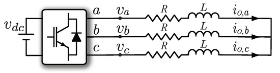
Figure 1.
Three-phase two-level inverter with RL (resistive-inductive) load diagram.

Table 1.
System variables and parameters.
The system dynamic equations in the -frame are the following,
where and . Here, , where is the switching state of the inverter expressed in the -frame.
In state-space representation, this model can be summarized with the expression
where ; ; ; . Here, is the identity matrix with dimension.
2.2. Control Algorithm
Using the discrete state space representation of the continuous model presented in Section 2.1 as basis, the FCS-MPC algorithm is applied in each sampling interval. First, measurements are obtained and variables are transformed to the -frame. The output voltage generated by the VSI can be known from the measurement of the dc-link voltage and the currently applied switching state. When all the values for the state variables and the inputs of the system are known, a prediction for the next sampling interval () can be calculated. This first prediction is performed to compensate for the digital implementation delay [34].
Then, an Exhaustive Searching Algorithm (ESA) is applied to check all the possible switching states in the interval, which are the input to the system. For the proposed FCS-MPC scheme and the VSI in this application, the control input can be considered as a discrete variable with a finite number of possible values. In particular, there are eight possible switching states, where two of them are identical. Computing predictions for the possible switching states in the interval, the possible values for the system state variables in the instant are found. The optimal switching state for the interval can be chosen and stored to be applied in the instant. The selection of the optimal switching state is based in the evaluation of a cost function that can be formulated to take many factors into account. In this case, as the target will be to accomplish the tracking of an output current reference, the first term in the cost function consists in the calculation of the error in the output current. Also, a switching limiting term is considered in the cost function. The goal of this term is to penalize the switching effort of the FCS-MPC algorithm. Therefore, a possible switching state that might be optimal according to the first term may be discarded due to the additional cost introduced by the second term. As a consequence of the algorithm formulation, the resulting switching frequency is not a fixed value, as the same switching state can be the optimal in consecutive sampling instants. Thus, the cost function is designed as
where is the -frame current reference in the sampling interval ; is the -frame current prediction for the sampling interval ; and are the switching states in the sampling intervals k and , respectively. The parameter is a weighting factor which adjusts the importance of the second term in the cost function [9,10]. Higher values provide a greater penalization of the switching effort over the current tracking error. In consequence, they will generate a lower switching frequency in average.
3. Digital Design
This section presents the proposed HW/SW design for the selected FPSoC platform. The Xilinx Vivado software is used to design the hardware and software applications [35].
3.1. Configuring FPSoC Resources
As explained in Section 1, the target platform for this work is a Xilinx Zynq 7000 FPSoC running on a Zedboard evaluation kit [36]. Care must be taken to distribute tasks between the different resources available in this platform. Basically, the system is composed of a dual-core ARM Cortex-A9 processing system (PS) that can run up to 667 MHz and an Artix-7 FPGA-based programmable logic (PL). Shared memory resources, such as DDR3 Memory and On-Chip Memory (OCM), are available to share information between the FPGA side and the two processors. The data sharing process between the components is handled by a low latency AXI interface [37].
In this implementation, three main tasks are executed periodically: First, measurements of the electrical magnitudes are sampled in every control interval. An external analog-to-digital converter (ADC) is used for this purpose. Specifically, the 12-bit, 16 sequential channels, SAR, Texas Instruments ADS7953 [38]. Communications between the ADC and the control platform are based on the SPI protocol. Therefore, management of the ADC through the SPI protocol becomes one of the main tasks to be performed by the system. When all the measurements are available, the second task can be executed, which is the control algorithm itself. Finally, a third task consisting of external communications, which permit the interaction and data transfers from and to the system, has to be performed. The way these three main tasks are addressed is not trivial, as critical tasks like measurements and control algorithm calculations require real-time execution, not ensured by an operating system in general. External communications are not a critical task, thus being able to take advantage of an operating system-based solution without suffering its drawbacks.
To solve this, the structure depicted in Figure 2 is proposed. One of the ARM cores executes a baremetal application that has access to the SPI peripheral and handles communication with the external ADC. A different design alternative would be to implement a custom peripheral in the programmable logic to handle the SPI communications. This option would be interesting if many parallel ADCs were used in this application, as the FPGA would be capable of implementing many of these SPI blocks in parallel. The decision to use the built-in peripheral in the ARM processor was made to highlight the usefulness of an FPSoC system compared to just an FPGA. Not everything must be designed in the hardware by the programmer, as peripherals included in the SoC can be used, which is usually a simpler solution for the designer and does not occupy extra resources in the FPGA. Also, only one SPI interface is used in this application, which the built-in SPI peripheral is perfectly capable of handling.
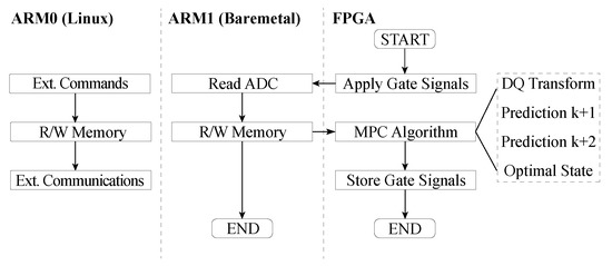
Figure 2.
Flowchart of the general implementation.
The CPU in charge of the baremetal application is interrupted by means of its private interruption channels by a signal from the FPGA. This event triggers the execution of an interrupt service routine where readings from the ADC are performed. When measurements are completed, they are written to specific registers in the shared DDR3 memory through an AXI4-Lite protocol implemented in one of the two 32-bit Master AXI ports available. This interface allows low latency and high bandwidth communications between the PS and the PL. These memory registers are then directly wired to internal signals in the FPGA.
After this, the control algorithm must be calculated. This task is performed by the FPGA. All calculations in the algorithm are performed as fixed point operations; this is because using floating point arithmetics in a FPGA design is much more demanding when it comes to power and resources consumption [39]. 16-bit word length is used for the calculations of the implemented algorithm. Our quantization error is mostly defined by the 12-bit measurements that can be obtained from the system with the selected ADC. 16-bit fixed-point variables are used to have enough overhead in the calculations, avoiding the introduction of extra errors. The stability and accuracy of the algorithm is tested through MATLAB simulations, before the VHDL implementation for the FPGA. For these simulations, a C-code version of the algorithm is also executed using 16-bit integers. The basic methodology is to internally work with every variable in the algorithm within a desired integer scale, and latter obtain their real number correspondence by re-scaling, only when needed for graphical representation. Using 16-bit variables allows an efficient use of the 32-bit bus width used for memory sharing, as two variables may exactly fit in one register.
The programmable logic side also implements a hardware counter that governs the system’s timing and which is used to interrupt the CPU every sampling interval. The firing pulses are stored in the FPGA when the optimal switching state is selected and applied at the beginning of the next sample interval. A simple Finite-State Machine (FSM) implemented in the FPGA is in charge of operating the system, executing commands sent through a graphical user interface running in a PC.
The other ARM core available in the system takes care of communications. To make full use of the system, a Linux distribution supplied by Xilinx, called Petalinux [40], is compiled and built making the necessary customizations to work along with the other CPU with no problems. This configuration is called “Asymmetric Multiprocessing” (AMP) and allows each core to run independent software stacks and executables [41]. Beyond the guidelines proposed in [41], special care must be taken when configuring the devicetree of the Petalinux OS. Default compilations supplied by Xilinx are made aware of peripherals included in the SoC. In particular, modifications to reserve exclusive access for ARM1 (baremetal application) to the software side GPIOs and one of the SPI controllers were necessary in this case. Detailed instructions to compile and modify the Petalinux OS can be found in [42].
By running AMP with both a Petalinux OS in CPU0 and a baremetal application in CPU1, this platform becomes a great embedded solution that combines the flexibility of low-level baremetal applications to easily control peripherals and high level solutions provided by an operating system. In particular, an application executes in the Petalinux OS to communicate through TCP/IP protocol, transferring data using an Ethernet connection to the user interface executed in a PC. This user interface is built in order to allow the monitoring of the system and sending commands to the FSM implemented in the FPGA.
3.2. FPGA Implementation
In this case, an HDL-based solution is carried out to perform the control algorithm. A block diagram of the proposed hardware design is offered in Figure 3. This diagram includes the FSM block and the counter described in Section 3.1, together with the rest of the designed blocks.
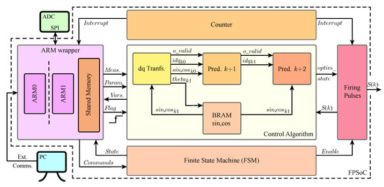
Figure 3.
Block diagram of the proposed architecture.
The first step in the design is to include a wrapper block (“ARM Wrapper”) for the processing system (PS) in the hardware design. In this wrapper, the Zynq PS from the intellectual property cores (IP) library in Vivado must be added alongside all the auxiliary I/O blocks that can be used to interconnect PS ports with FPGA signals. Within this wrapper we define a customized peripheral, created using Vivado’s IP tools, which will be used to solve the data sharing between the PS and PL. This peripheral consists of a series of 32-bit memory registers that are associated to specific addresses in shared memory space, so they can also be read and written by applications executed in the ARM. This peripheral is accessed from both the PL and the PS through an AXI4-Lite interface [37].
As it was described in Section 3.1, the FPGA has access to every measurement once they are written to the shared memory. In this application, the FPGA notices this event by toggling a bit of a register in memory (“”), which triggers a chain of operations until the optimal switching state for the next sampling interval is achieved.
These operations can be organized in three main blocks that must work sequentially as the calculations of the previous block are needed for the next one. These three blocks are shown in Figure 3. They are from first to last: Clarke and Park’s transformation (“dq Transf.”, see Figure 4 for more details), Prediction to (“Pred. k+1”), and Prediction to (“Pred. k+2”). A valid data signal (“”) is propagated through the datapath to indicate that output data from each block is ready.
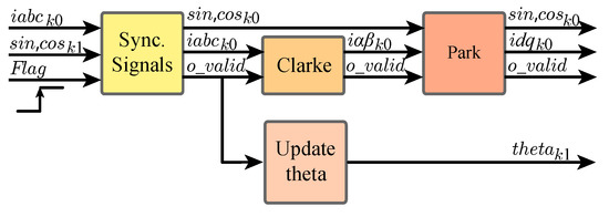
Figure 4.
Block diagram of the hardware design for transformation block (dq Transf).
Transformation and Prediction to blocks are performed in order to obtain the -frame representation of the system variables and to compensate for the digital delay, respectively.
The implementation of these blocks is straightforward as they consist solely of a series of arithmetic operations. In our fixed-point algorithm, these operations are reduced to a series of simple sums, subtractions and multiplications between 16-bit integer numbers. To calculate sine and cosine functions for the corresponding phase angle, many different alternatives are at the designer’s disposal. IP cores that implement CORDIC algorithms are available in the Xilinx IP library. This option is discarded because of the extra latency introduced in the calculations by this method and because of the extra need for FPGA logic resources. Another option could be the use of a polynomial approximation of these functions, which could simplify the calculation of these trigonometric functions to a series of more simple calculations, but FPGA logic resources should also be spent on these calculations. The proposed solution in this paper is the use of RAM block resources. In particular, a RAM block with 4095 16-bit values is implemented (“BRAM sin,cos”). Several simulations were run through Matlab/Simulink to achieve the minimum number of values to be stored in memory that does not translate into a noticeable degradation of the resulting waveforms due to loss of accuracy. This block is fed with a 12 bits binary radians angle, which corresponds with the phase for the sampling interval, therefore obtaining sine and cosine values for (“”). For the k sampling interval, sine and cosine (“”) are obtained introducing a one step digital delay as shown in Figure 4.
With this solution, we infer a block RAM to store these values, instead of using other types of FPGA resources that would be preferably saved for other tasks. Coding guidelines for RAM blocks proposed in [43] must be followed to achieve this. Note that logic slices can also be inferred by the synthesis tool to store data (this is known as “distributed RAM”). Therefore, following the [43] guidelines, it is necessary to help the synthesizer select the required type of resource for our memory block.
The remaining operations can be expressed as a set of sums and multiplications that can be performed as a combinational circuit within each block. A synchronous flip-flop in the output of each block ensures synchronization of the datapath between blocks. The latency for the implemented blocks allows for the calculation of each one of these blocks in one clock cycle, when a 10 ns period clock is used. This ensures the availability of the results for the operation of the following block in the next clock cycle.
The implementation of the prediction is not so immediate. The optimal state (“”) must be selected by minimizing the cost function (4). This optimization is performed by an ESA, which computes the necessary predictions for the instant and their associated cost. Then, the value of the cost function for every possible candidate state is compared so the minimum can be selected. It is the need for this iteration what causes the high computational burden in the control algorithm, as the number of calculations grow exponentially as the number of prediction horizons increases. Two possible solutions are discussed here.
3.2.1. Parallel Prediction
In this case, a completely parallel implementation for the prediction will be described. As depicted in Figure 5, this approach consists of dividing every iteration of the loop that checks every possible state into hardware blocks that are in charge of calculating one prediction for one given state. Therefore, if eight predictions must be made for , there will be eight identical blocks. Every block calculates the value for the cost function. A combinational comparator reads these values and selects the optimal switching state. Due to the architecture for this method, there is no need for pipelining and synchronous flip-flops placed in the output of every calculation block can be eliminated. This avoids the wait for a clock cycle after each block, decreasing calculation time. Opposed to that, all calculation blocks are inferred as combinational circuits whose results are propagated until a final optimal state for the next sampling interval is achieved.
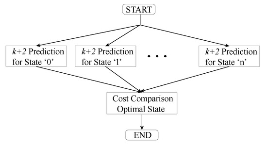
Figure 5.
Flowchart of the Parallel Field-Programmable Gate Array (FPGA) Implementation for the Exhaustive Searching Algorithm (ESA).
This is the fastest solution when it comes to calculation time, but a great area consumption is expected from this implementation. Further statistics can be found in Section 5.
3.2.2. Sequential Prediction
In opposition to the previously described solution, a completely sequential design for the prediction with only one prediction block could be adopted. Now, a pipeline structure that controls the access to the aforementioned block is necessary to ensure its availability and the validity of the results. This method is implemented with an FSM which is responsible of sequentially checking every possible state by feeding the state to be calculated to the prediction block. Unlike the parallel solution, synchronous processes must be used to synchronize results with the clock signal. A flowchart for this method can be seen in Figure 6.
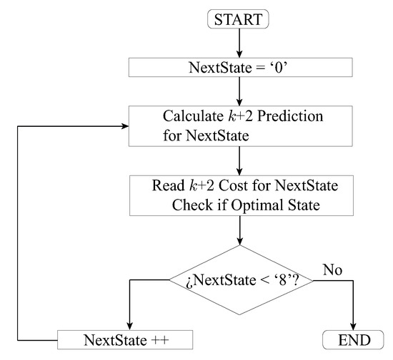
Figure 6.
Flowchart of the Sequential FPGA Implementation for the ESA.
With this solution, area consumption can be greatly reduced by decreasing the number of blocks to just one. Also, a comparator block with eight inputs is not necessary now since one of the states in the FSM can be used to compare every cost to the current optimal cost. The main drawback of this implementation is the longer time required to compute every prediction.
Finally, when the optimal switching state for the next control interval is obtained, this state is stored in a register until the counter, in charge of the system timing, signals the end of the control interval. The block “Firing Pulses” ensures the synchronization of the gate signals, and feeds the system with its current state (“”).
4. Experimental Results: Verification of the Proposed Implementation
This section is dedicated to the verification of the actual performance for the designed controller running in the Zedboard evaluation kit, which can be seen in Figure 7. Experiments are carried out with a two-level three-phase inverter connected to a fixed load. Parameters of the system for these experiments are shown in Table 2.
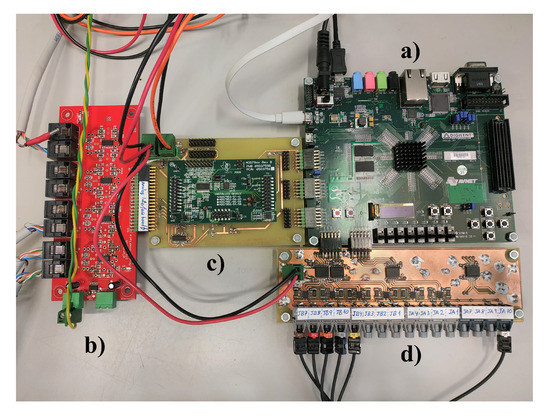
Figure 7.
Zedboard evaluation module (a) for Zynq 7000 SoC with custom daughter board for sensors level shifter (b), ADS7953 interface board (c), and fiber optics board for gate signals (d).
Table 2.
System variables and parameters.
As it can be seen in Figure 8, the designed controller for both implementations achieves steady-state operation with fast dynamic response and low distortion when the reference amplitude for the abc-frame output currents is changed from 1 A to 2 A. Results for the parallel method appear in Figure 8a,b and in the sequential method, so that the equivalency of both implementations can be checked. Measurements for the spectrum magnitude achieved in the output currents are also made with the Fluke 434 Series II power quality analyzer. The resulting THD is for both methods. Also, the average switching frequency is 7 kHz (with switching limiting term equal to zero). This value is measured by counting the number of switch events in one grid cycle (20 ms). Finally, calculation times for the implemented algorithm in the FPGA are measured. This information is obtained by toggling a digital output port in the FPGA when calculations for the algorithm start and end. The achieved calculation times are 50 ns for the parallel design and 400 ns for the sequential implementation. As expected, the behavior of both implementations is the same when the output current quality and control performance are considered. Nonetheless, calculation time is reduced by a great margin with the parallel implementation, when compared to the sequential design.
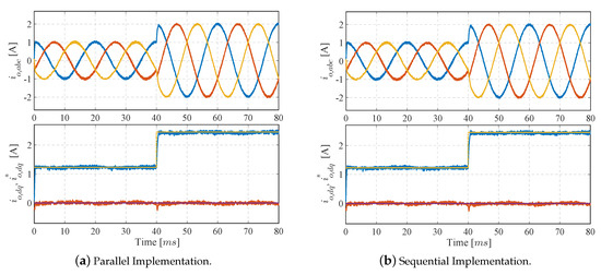
Figure 8.
Experimental results: Output currents in abc and dq-frame. At ms, the reference amplitude for the abc-frame current changes from 1 A to 2 A.
5. Area, Calculation Time, and Consumption discussion
In this section, different statistics for the proposed hardware designs are analyzed. A comparison between the parallel and the sequential implementations is carried out to check the main differences between both proposed solutions. The availability of different resources in the Artix-7 FPGA give designers the flexibility to decide in what proportion they are used by configuring synthesis settings. Among these resources, we can find configurable logic blocks (CLB), DSP cells, and RAM blocks.
A CLB is the basic logic block resource to implement logic operations in an FPGA design. In Xilinx’s Artix-7 FPGAs, these blocks are composed of two slices. There are two different types of slices: SLICEL and SLICEM. SLICEL can only be used to implement logical and arithmetic operations. SLICEM can also be used as data storage (“distributed RAM”). Within these slices there are logic elements like Look-up tables (LUT), which implement combinatorial logic and flip-flop registers (FF cells), allowing clock synchronization to implement sequential logic [44]. These resources are automatically inferred by the synthesis tool for most basic operations.
DSP blocks (DSP48E1 in Artix-7 Xilinx FPGAs) are dedicated slices for the implementation of arithmetic operations [45]. They are intended for intense digital signal processing applications. Without DSP blocks, designs for these types of applications would quickly run out of other resources like LUTs or FF Cells. By default, the synthesizer infers DSP blocks for operations such as multiplication, multiplication–addition, multiplication–subtraction, and multiplication–accumulate. Different options for the synthesis tool may be used to alter this default behavior [43].
BRAM are memory resources provided in the Artix-7 FPGAs that allow data storage of up to 36 Kb [46]. Inferring these resources to store large amounts of data reduces the consumption of CLB resources that may be used for logic operations.
In the utilization reports, we will measure the area consumption in terms of utilized LUT, FF Cells, DSP blocks, and BRAM. A greater number of utilized resources means a higher area consumption for the FPGA implementation. A hierarchical utilization report is offered in Table 3 for the parallel design and in Table 4 for the sequential design. Vivado default settings are used for this first approach. For the prediction block, resource consumption for auxiliary blocks (like a secondary FSM for the sequential method, or a comparator for the parallel method) are included. Resources for other secondary blocks are offered under the term “Miscellaneous”. Also note that most of the resource utilization by the ARM wrapper block are fixed by proprietary designs provided by Xilinx in their IP cores.
Table 3.
Hierarchical utilization for parallel method.
Table 4.
Hierarchical utilization for sequential method.
As it can be seen, sequential implementation reduces FPGA resources consumption at the expense of a greater calculation time. In consequence, power consumption and temperatures are also reduced with the sequential alternative. Reduction in FPGA resources allows the same architecture to be implemented in a more affordable FPGA. In addition, there is more room to increase the complexity of the control algorithm with a higher number of states or more prediction horizons.
Another interesting fact that can be appreciated in the implementation results is the high usage of DSP Cells. Many multiplications are calculated during the FCS-MPC algorithm, so this behavior is expected. Nonetheless, as the usage of DSP Cells gets closer to the FPGA limit for this specific resource, the synthesizer decides to perform some of these operations with LUT resources. Therefore, a comparison between both designs is not so straightforward. For this reason, another implementation is performed by forcing the synthesizer to infer LUT resources to perform all these operations. Restricting the synthesis process to force no usage of DSP cells, a better and easier to extrapolate measurement of the area consumption for both designs can be obtained. This is also helpful to extrapolate the resource consumption of the proposed design to FPGAs with no DSP cells. Results for this implementation are offered in Table 5 for the parallel design and in Table 6 for the sequential design. High area optimization directive was used in this case.
Table 5.
Hierarchical utilization for parallel method. No Digital Signal Processing (DSP) cells.
Table 6.
Hierarchical utilization for sequential method. No DSP cells.
Finally, to put into perspective the achieved calculation times in both proposed designs, the same algorithm implemented in the FPGA was also implemented in a DSP. Particularly, the Texas Instruments, Delfino C2000 TMS320F28335 digital signal microcontroller was used. Executing the same algorithm with a 150 MHz clock, and compiling the application with all the compiler optimizations configured for maximum speed, a 12 s calculation time for the FCS-MPC algorithm was achieved, which is 30 times the calculation time than the slowest proposed FPGA design and 240 times the calculation time when compared to the fastest proposed design, as it can be seen in Table 7. The execution time is not accounting the need for external communications. This fact benefits the FPSoC solution, as one of the ARM cores executes this task in parallel, as the other core runs critical tasks for the control algorithm. In the DSP, there is no such possibility and some time must be allocated to execute non-critical tasks. Thus, the achievable sampling frequency with a DSP-based solution is much more limited. Note that the FPGA design has been tested with a 100 MHz clock.
Table 7.
Calculation time for proposed methods.
6. Experimental Results: High Sampling Frequency Evaluation
To better illustrate the capabilities of the proposed solution, additional experiments are shown in this section. The idea is to demonstrate the benefits that can be achieved by being able to increase the sampling frequency at which the control algorithm is executed. The sequential solution proposed in this work is used for the experiments presented in this section, as both solutions achieve the same results, as demonstrated in Section 4. In these experiments, we use the switching effort term to obtain a desired steady-state average switching frequency (). The corresponding tuning parameter used in each experiment is specified in each figure. First, two experiments limiting the switching frequency to kHz are provided to compare these results with higher sampling frequency experiments.
As can be seen in Figure 9, the steady-state performance for the current error tracking is deteriorated and the harmonic distortion is increased as the switching effort is more penalized in the experiment. In Figure 10, the same experiment is repeated for a sampling frequency of 80 kHz and 140 kHz. Note that for an equal average switching frequency, a higher sampling frequency can improve the results of the generated currents while maintaining the same switching effort, i.e., the switching losses remain identical while improving the FCS-MPC performance.
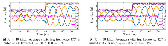
Figure 9.
Experimental results at sampling frequency kHz: Output currents in abc and dq-frame. At ms, the reference amplitude for the abc-frame current changes from 1 A to 2 A.
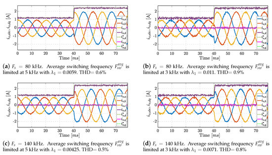
Figure 10.
Experimental results at high sampling frequency: Output currents in abc and dq-frame. At ms, the reference amplitude for the abc-frame current changes from 1 A to 2 A.
7. Conclusions
In this paper, an FCS-MPC strategy implementation for an FPSoC platform has been developed and validated as proof of all the possibilities that these platforms offer for new power electronics applications. First, a new general HW/SW architecture for the programming of the FPSoC resources has been proposed. This architecture takes full advantage of all the possibilities of the system by efficiently distributing the execution of all the necessary tasks. Also, two methods for the implementation of the control algorithm in the FPGA have been discussed and compared. Their advantages and drawbacks have been contrasted when it comes to variables like calculation time or area consumption. Both proposals were proven to be feasible solutions. Each of them could be better suited depending on the application and system restrictions and requirements. For the two proposed alternatives, the results show that in order to facilitate the adoption of complex control algorithms with a high bandwith and Wide Band-gap semiconductors in most modern power electronics designs, migrating from conventional DSP platforms to new FPSoC devices is as a really interesting approach, as calculation times can be greatly reduced. As proof of the benefits of this reduction, the proposed design is tested with additional experiments with sampling frequency values that are unattainable by the DSP counterpart. It is demonstrated that for identical switching frequencies (switching losses remaining the same), the steady-state performance of the FCS-MPC is improved by reducing the harmonic distortion of the resulting output currents.
Future works will be focused in the development of new designs that combine the advantages from both types of designs, optimizing the area–speed trade-off. Testing the capabilities of the proposed implementation with more complex control strategies and with new power converter prototypes based in modern semiconductor technologies for high switching frequency applications will also be the focus of the authors’ attention.
Author Contributions
Conceptualization, E.Z., S.V., H.G.M.; Methodology, E.Z., S.V., H.G.M., J.A.S., A.M.; Software, E.Z., S.V., H.G.M., J.A.S., A.M.; Validation, E.Z., S.V., H.G.M.; Investigation, E.Z., S.V., H.G.M., J.A.S., A.M., J.I.L., L.G.F.; Resources, E.Z., S.V., A.M., J.I.L., L.G.F.; Writing-Original Draft Preparation, E.Z.; Writing-Review and Editing, E.Z., S.V., H.G.M., A.M., J.I.L., L.G.F.; Supervision, S.V., H.G.M., A.M., J.I.L. and L.G.F.; Project Administration, S.V., J.I.L. and L.G.F. All authors have read and agreed to the published version of the manuscript.
Funding
The authors gratefully acknowledge the financial support provided by Spanish Ministry of Economy and Competitivity under the project TEC2016-78430-R. Section 4 and Section 5 were made possible by NPRP 9-310-2-134 from the Qatar National Research Fund (a member of Qatar Foundation). The statements made herein are solely the responsibility of the authors.
Conflicts of Interest
The authors declare no conflicts of interest.
References
- Leon, J.I.; Vazquez, S.; Franquelo, L.G. Multilevel Converters: Control and Modulation Techniques for Their Operation and Industrial Applications. Proc. IEEE 2017, 105, 2066–2081. [Google Scholar] [CrossRef]
- Romero-Cadaval, E.; Spagnuolo, G.; Franquelo, L.G.; Ramos-Paja, C.A.; Suntio, T.; Xiao, W.M. Grid-Connected Photovoltaic Generation Plants: Components and Operation. IEEE Ind. Electron. Mag. 2013, 7, 6–20. [Google Scholar] [CrossRef]
- Vazquez, S.; Marquez, A.; Aguilera, R.; Quevedo, D.; Leon, J.I.; Franquelo, L.G. Predictive Optimal Switching Sequence Direct Power Control for Grid-Connected Power Converters. IEEE Trans. Ind. Electron. 2015, 62, 2010–2020. [Google Scholar] [CrossRef]
- Wang, G.; Konstantinou, G.; Townsend, C.D.; Pou, J.; Vazquez, S.; Demetriades, G.D.; Agelidis, V.G. A Review of Power Electronics for Grid Connection of Utility-Scale Battery Energy Storage Systems. IEEE Trans. Sustain. Energy 2016, 7, 1778–1790. [Google Scholar] [CrossRef]
- Baidya, R.; Aguilera, R.P.; Acuna, P.; Vazquez, S.; du Toit Mouton, H. Multistep Model Predictive Control for Cascaded H-Bridge Inverters: Formulation and Analysis. IEEE Trans. Power Electron. 2018, 33, 876–886. [Google Scholar] [CrossRef]
- Vazquez, S.; Leon, J.I.; Franquelo, L.G.; Rodriguez, J.; Young, H.A.; Marquez, A.; Zanchetta, P. Model Predictive Control: A Review of Its Applications in Power Electronics. IEEE Ind. Electron. Mag. 2014, 8, 16–31. [Google Scholar] [CrossRef]
- Majmunovic, B.; Dragicevic, T.; Blaabjerg, F. Multi Objective Modulated Model Predictive Control of Stand-Alone Voltage Source Converters. IEEE J. Emerg. Sel. Top. Power Electron. 2019. [Google Scholar] [CrossRef]
- Bordons, C.; Montero, C. Basic Principles of MPC for Power Converters: Bridging the Gap Between Theory and Practice. IEEE Ind. Electron. Mag. 2015, 9, 31–43. [Google Scholar] [CrossRef]
- Vazquez, S.; Rodriguez, J.; Rivera, M.; Franquelo, L.G.; Norambuena, M. Model Predictive Control for Power Converters and Drives: Advances and Trends. IEEE Trans. Ind. Electron. 2017, 64, 935–947. [Google Scholar] [CrossRef]
- Karamanakos, P.; Geyer, T. Guidelines for the Design of Finite Control Set Model Predictive Controllers. IEEE Trans. Power Electron. 2019. [Google Scholar] [CrossRef]
- Vazquez, S.; Acuna, P.; Aguilera, R.P.; Pou, J.; Leon, J.I.; Franquelo, L.G. DC-Link Voltage Balancing Strategy Based on Optimal Switching Sequences Model Predictive Control for Single-Phase H-NPC Converters. IEEE Trans. Ind. Electron. 2019. [Google Scholar] [CrossRef]
- Stellato, B.; Geyer, T.; Goulart, P.J. High-Speed Finite Control Set Model Predictive Control for Power Electronics. IEEE Trans. Power Electron. 2017, 32, 4007–4020. [Google Scholar] [CrossRef]
- Kouro, S.; Perez, M.A.; Rodriguez, J.; Llor, A.M.; Young, H.A. Model Predictive Control: MPC’s Role in the Evolution of Power Electronics. IEEE Ind. Electron. Mag. 2015, 9, 8–21. [Google Scholar] [CrossRef]
- Mekonnen, E.T.; Katcha, J.; Parker, M. An FPGA-based digital control development method for power electronics. In Proceedings of the IECON 2012—38th Annual Conference on IEEE Industrial Electronics Society, Monteral, QC, Canada, 25–28 October 2012; pp. 222–226. [Google Scholar] [CrossRef]
- Gulbudak, O.; Santi, E. FPGA-Based Model Predictive Controller for Direct Matrix Converter. IEEE Trans. Ind. Electron. 2016, 63, 4560–4570. [Google Scholar] [CrossRef]
- He, N.; Chen, M.; Wu, J.; Zhu, N.; Ge, D.X. 20 kW Zero-Voltage-Switching SiC-MOSFET Grid Inverter with 300 kHz Switching Frequecny. IEEE Trans. Power Electron. 2018. [Google Scholar] [CrossRef]
- Yin, S.; Tseng, K.J.; Liu, Y.; Simanjorang, R.; Tong, C.F.; Gupta, A.K. Demonstration of a 50 kW and 100 kHz SiC high power density converter for aerospace application. In Proceedings of the 2016 IEEE Region 10 Conference (TENCON), Singapore, 22–25 November 2016; pp. 2888–2891. [Google Scholar] [CrossRef]
- Tarisciotti, L.; Costabeber, A.; Linglin, C.; Walker, A.; Galea, M. Evaluation of isolated DC/DC converter topologies for future HVDC aerospace microgrids. In Proceedings of the 2017 IEEE Energy Conversion Congress and Exposition (ECCE), Cincinnati, OH, USA, 1–5 October 2017; pp. 2238–2245. [Google Scholar] [CrossRef]
- Qian, W.; Zhang, X.; Jin, F.; Bai, H.; Lu, D.; Cheng, B. Using High-Control-Bandwidth FPGA and SiC Inverters to Enhance High-Frequency Injection Sensorless Control in Interior Permanent Magnet Synchronous Machine. IEEE Access 2018, 6, 42454–42466. [Google Scholar] [CrossRef]
- Jin, F.; Bai, H.; Lu, D.; Cheng, B. Maximizing Potentials of SiC Inverters for Permanent Magnet Synchronous Motor Control By Using FPGA. In Proceedings of the 2018 IEEE 6th Workshop on Wide Band-gap Power Devices and Applications (WiPDA), Atlanta, GA, USA, 31 October–2 November 2018; pp. 259–263. [Google Scholar] [CrossRef]
- Monmasson, E.; Cirstea, M.N. FPGA Design Methodology for Industrial Control Systems A Review. IEEE Trans. Ind. Electron. 2007, 54, 1824–1842. [Google Scholar] [CrossRef]
- Zhang, Y.; Yuan, X.; Wu, X.; Yuan, Y.; Zhou, J. Parallel Implementation of Model Predictive Control for Multilevel Cascaded H-Bridge STATCOM with Linear Complexity. IEEE Trans. Ind. Electron. 2019. [Google Scholar] [CrossRef]
- Naouar, M.; Monmasson, E.; Naassani, A.A.; Slama-Belkhodja, I.; Patin, N. FPGA-Based Current Controllers for AC Machine Drives: A Review. IEEE Trans. Ind. Electron. 2007, 54, 1907–1925. [Google Scholar] [CrossRef]
- Monmasson, E.; Idkhajine, L.; Naouar, M.W. FPGA-based Controllers. IEEE Ind. Electron. Mag. 2011, 5, 14–26. [Google Scholar] [CrossRef]
- Navarro, D.; Lucia, O.; Barragan, L.A.; Urriza, I.; Jimenez, O. High-Level Synthesis for Accelerating the FPGA Implementation of Computationally Demanding Control Algorithms for Power Converters. IEEE Trans. Ind. Inform. 2013, 9, 1371–1379. [Google Scholar] [CrossRef]
- Velazquez, R.; Lucia, O.; Navarro, D.; Barragan, L.A.; Artigas, J.I.; Sagues, C. Design of an FPGA-based full-state feedback controller using high level synthesis tools. In Proceedings of the 2014 IEEE 15th Workshop on Control and Modeling for Power Electronics (COMPEL), Santander, Spain, 22–25 June 2014; pp. 1–6. [Google Scholar] [CrossRef]
- Martin, G.; Smith, G. High-Level Synthesis: Past, Present, and Future. IEEE Des. Test Comput. 2009, 26, 18–25. [Google Scholar] [CrossRef]
- Molanes, R.F.; Rodriguez-Andina, J.J.; Farina, J. Performance Characterization and Design Guidelines for Efficient Processor-FPGA Communication in Cyclone V FPSoCs. IEEE Trans. Ind. Electron. 2018, 65, 4368–4377. [Google Scholar] [CrossRef]
- Stanciu, A.; Gerigan, C. Comparison between implementations efficiency of HLS and HDL using operations over Galois Fields. In Proceedings of the 2017 IEEE 23rd International Symposium for Design and Technology in Electronic Packaging (SIITME), Constanta, Romania, 26–29 October 2017; pp. 171–174. [Google Scholar] [CrossRef]
- Pelcat, M.; Bourrasset, C.; Maggiani, L.; Berry, F. Design productivity of a high level synthesis compiler versus HDL. In Proceedings of the 2016 International Conference on Embedded Computer Systems: Architectures, Modeling and Simulation (SAMOS), Samos, Greece, 17–21 July 2016; pp. 140–147. [Google Scholar] [CrossRef]
- Sanchez, F.M.; Mateos, R.; Bueno, E.J.; Mingo, J.; Sanz, I. Comparative of HLS and HDL implementations of a grid synchronization algorithm. In Proceedings of the IECON 2013—39th Annual Conference of the IEEE Industrial Electronics Society, Vienna, Austria, 10–13 November 2013; pp. 2232–2237. [Google Scholar] [CrossRef]
- Bahri, I.; Idkhajine, L.; Monmasson, E.; Benkhelifa, M.E.A. Hardware/Software Codesign Guidelines for System on Chip FPGA-Based Sensorless AC Drive Applications. IEEE Trans. Ind. Inform. 2013, 9, 2165–2176. [Google Scholar] [CrossRef]
- Xilinx. Zynq-7000 SoC Data Sheet: Overview. Available online: https://www.xilinx.com/support/documentation/data_sheets/ds190-Zynq-7000-Overview.pdf (accessed on 30 January 2020).
- Cortes, P.; Rodriguez, J.; Silva, C.; Flores, A. Delay Compensation in Model Predictive Current Control of a Three-Phase Inverter. IEEE Trans. Ind. Electron. 2012, 59, 1323–1325. [Google Scholar] [CrossRef]
- Xilinx. Vivado Design Suite. Available online: https://www.xilinx.com/products/design-tools/vivado.html (accessed on 30 January 2020).
- Avnet. Zedboard Hardware User’s Guide. Available online: http://zedboard.org/sites/default/files/documentations/ZedBoard_HW_UG_v2_2.pdf (accessed on 30 January 2020).
- ARM. AMBA Specification. Available online: https://www.arm.com/products/silicon-ip-system/embedded-system-design/amba-specifications (accessed on 30 January 2020).
- TexasInstruments. ADS 7953 Datasheet. Available online: http://www.ti.com/lit/ds/symlink/ads7953.pdf (accessed on 30 January 2020).
- Finnerty, A.; Ratigner, H. Reduce Power and Cost by Converting from Floating Point to Fixed Point; Xilinx Inc.: Austin, TX, USA, 2017; pp. 1–14. [Google Scholar]
- Xilinx. Petalinux Tools. Available online: https://www.xilinx.com/products/design-tools/embedded-software/petalinux-sdk.html (accessed on 30 January 2020).
- Xilinx. Simple AMP Running Linux and Bare-Metal System on Both Zynq SoC Processors. Available online: https://www.xilinx.com/support/documentation/application_notes/xapp1078-amp-linux-bare-metal.pdf (accessed on 30 January 2020).
- Xilinx. Xilinx Wiki. Available online: https://xilinx-wiki.atlassian.net/wiki/spaces/A/overview (accessed on 30 January 2020).
- Xilinx. Vivado Design Suite User Guide: Synthesis. UG901. Available online: https://www.xilinx.com/support/documentation/sw_manuals/xilinx2017_1/ug901-vivado-synthesis.pdf (accessed on 30 January 2020).
- Xilinx. 7 Series FPGAs Configurable Logic Block. Available online: https://www.xilinx.com/support/documentation/user_guides/ug474_7Series_CLB.pdf (accessed on 30 January 2020).
- Xilinx. 7 Series DSP48E1 Slice. Available online: https://www.xilinx.com/support/documentation/user_guides/ug479_7Series_DSP48E1.pdf (accessed on 30 January 2020).
- Xilinx. 7 Series FPGAsMemory Resources. Available online: https://www.xilinx.com/support/documentation/user_guides/ug473_7Series_Memory_Resources.pdf (accessed on 30 January 2020).
© 2020 by the authors. Licensee MDPI, Basel, Switzerland. This article is an open access article distributed under the terms and conditions of the Creative Commons Attribution (CC BY) license (http://creativecommons.org/licenses/by/4.0/).