Article

A High-Efficiency and Wide-Input Range RF Energy Harvester Using Multiple Rectenna and Adaptive Matching †

1
Department of Electrical and Computer Engineering, University of California at San Diego, La Jolla, CA 92093, USA
2
Department of Electrical and Computer Engineering, Sungkyunkwan University, Suwon 16419, Korea
3
Nanoelectronics Group, Department of Informatics, University of Oslo, 0316 Oslo, Norway
*
Author to whom correspondence should be addressed.
This paper is an extended version of our paper published in 2018 IEEE 61st International Midwest Symposium on Circuits and Systems Conference, Windsor, ON, Canada, 5–8 August 2018; pp. 436–439.
Energies 2020, 13(5), 1023; https://doi.org/10.3390/en13051023
Submission received: 15 January 2020 / Revised: 12 February 2020 / Accepted: 18 February 2020 / Published: 25 February 2020

Abstract

:
In this paper, a Radio Frequency (RF) energy harvester (EH) system for Internet of Things (IoT)-related applications is presented. The proposed EH architecture operates at 5.2 GHz band and utilizes multiple rectenna. This approach enhances the efficiency of the whole system over a wide dynamic RF input range. In the presented circuit, configuration of the rectenna is controlled by Field-Programmable Gate Array (FPGA) with respect to the input power level of the received RF input signal. In addition, an automatic adaptive matching based on the configuration of the rectenna, level of the received signal, and load current adjusts the matching network. The rectenna is realized through the Radio Frequency-Direct Current (RF-DC) converter composed of two Schottky diodes and generates the output DC voltage. Finally, a buck-boost converter provides the flattened and fixed voltage for the IoT and wearable devices. The 5.2 GHz band reconfigurable system demonstrates 67% high efficiency and 6.1 V output DC voltage where the power level of RF input is +20 dBm. The main application of the proposed structure is for charging wearable smart devices such as a smart watch and bracelet.

Graphical Abstract

1. Introduction

Nowadays, the Internet-of-Things (IoT) and Bluetooth low-energy (BLE) devices have made a smart environment by using wireless sensors and communication protocols. These technologies transmit data for making decisions related human issues, health cares, and automation of the facilities. Communication without any interruptions and long battery life are the most challenging requirements for these aims. Wireless sensors need continuous power, which, with the conventional methods, suffer from the short lifetime of the batteries. In addition, an energy harvester (EH) and low-power devices may not be installed under normal conditions, and their batteries cannot be changed easily [1,2]. Longer battery life and a system with no need to recharge demands a low-power and high-efficiency power management-integrated circuit (PMIC). In addition, chip area and external passive components such as inductors and capacitors are other design challenges. Generally, parasitic elements, printed circuit boards (PCBs), and line losses are the targets of improvements, while recent trends have focused on the integration of an energy harvester power management system, especially an Radio Frequency (RF) EH system with an IoT/wearable or RF transceiver system [3,4].
Due to problems associated with the replacement or recharging of batteries, self-powering based on an energy harvesting communication network is a critical demand for these wireless devices. The main focus of recent work is remote charging via an EH from a renewable source and optimizing the processing methods [1,2,3,4,5,6,7,8]. Besides thermal, solar, and wind energy sources for EH, recently, the presence of ambient radio frequency (RF) signals is becoming an appealing source for EH in portable devices. The capability of the RF signals in carrying information in wireless devices introduces the concept of simultaneous wireless information and power transfer (SWIPT). SWIPT offers a noticeable concept in the field of communication systems, which provides efficient energy and information transfer in addition to powering an RF EH system.
Figure 1 shows the top block diagram of an RF EH system for IoT/wearable applications. The antenna, rectifier, DC-DC converter, and load are the main building blocks of an RF EH system. The overall efficiency of the whole system is determined by the RF-to-DC and DC-DC converter efficiency. Based on the received power and converted DC voltage level, buck or boost modes would be selected. Providing a higher output DC voltage and using a simple highly efficient buck converter are preferable in comparison to a buck-boost converter. In contrast, enhancing the RF EH system overall efficiency requires the design of a high-output DC voltage rectifier with high power conversion efficiency (PCE).
This paper is organized as follows: The top system architecture and detailed building blocks of the proposed RF EH system are described in Section 2. Section 3 focuses on the implementation and experimental result. Section 4 concludes the paper.

2. Architectural and Detailed Building Blocks of the EF EH System
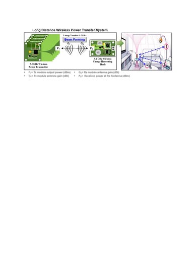
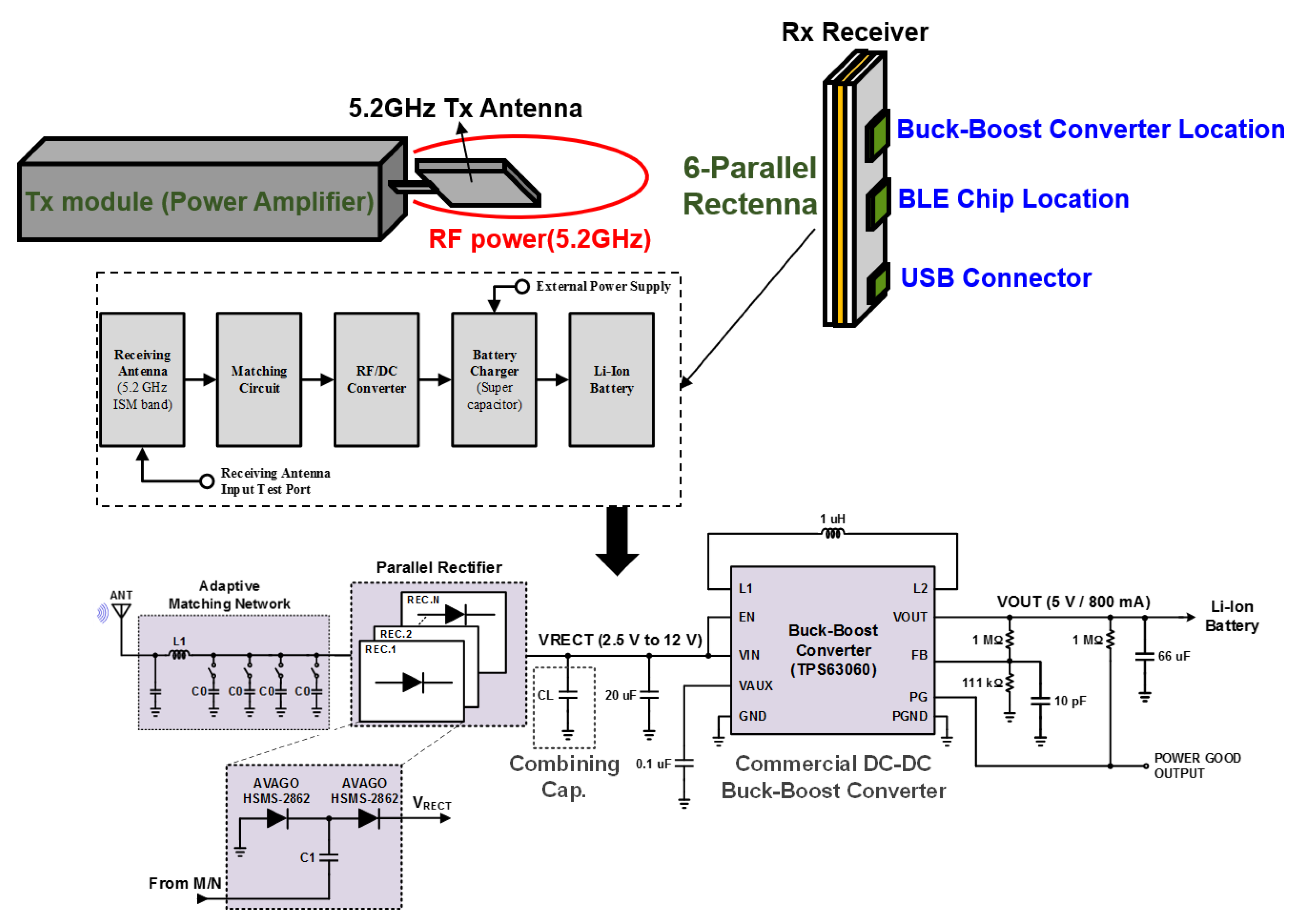
2.1. Architecture

Figure 2 indicates the system budget and path loss measurement vs. the distance of the RF EH system. The maximum available power at the Receiver (Rx) antenna is given by
P R = P T + G T + G R P a t h   l o s s
where, in the Tx module, PT and GT are the respective output power and antenna gain, and in the Rx module, GR and PR are the respective antenna gain and received power. Path loss is the air loss of the measured environment. Table 1 demonstrates the system budget considering an ideal system structure, the distance between Tx and Rx modules, and the free space path loss (FSPL) equation. To maximize the RF power level for RF-DC conversion and eliminate the air here, a 6-array antenna is designed. An automatically adapted and reconfigurable multiple rectenna architecture depending on the RF input signal level is presented.
Figure 3 illustrates a block diagram of the proposed RF EH system [8]. It comprises a 2 × 3 array patch antenna, 6-parallel RF-DC converter in the front side, DC-DC converter, BLE module, and Universal Serial Bus (USB) connector on the back side of the Rx module PCB board. The front view of the PCB has a rectenna composed of five RF-DC converters and five patch antennas; one RF-DC converter and one patch antenna are configured for the pilot signal only. The proposed RF-DC converter of each rectenna is fabricated based on a Dickson charge pump structure. A six-array rectenna with two Schottky diodes was adopted to produce high efficiency and high-output DC voltage. It has an optimized third harmonic source termination for an improved conversion efficiency, and the implemented RF-DC converter includes series transmission lines and open-stubs for the third harmonic inductive termination and fundamental impedance matching. The simulated third harmonic contour using the harmonic source-pull simulation shows an optimum region near jX75 Ω with a maximum efficiency of 69.45%. The optimum third harmonic impedance is inductive due to the junction capacitance of the Schottky diodes, and the input capacitance and inductive source impedance produce parallel resonance for an appropriate Class-F third harmonic termination. Compared to the efficiency of the rectifier without harmonic control, the proposed rectifier with harmonic control exhibits a 5.2% higher efficiency at an input power of about +20 dBm. Using the optimum third harmonic termination, the voltage waveforms across the Schottky diodes of RF-DC converters become closer to the square waves of an ideal RF-DC converter. The rectenna is the first block at the input of the Rx module to rectify the RF signal. A combining capacitor at the output of the rectenna is also used as a low-pass filter to remove ripples at the output. The output of the rectenna is fed to the buck-boost converter. In order to eliminate voltage variation, a buck-boost converter is used to produce constant output voltage. When the input voltage level reduces due to the weak RF signals, the boosting operation of the buck-boost converter is performed to maintain the output voltage level and vice-versa. A low drop-out (LDO) regulator can be used to maintain a constant output voltage. A super capacitor is connected at the output of the buck-boost converter to store energy and provides power for IoT/wearable devices and charging the battery.
The front and back sides of the EH system are implemented using RF-35 and FR4 with four layers through the commercial components to maximize the board efficiency. The multiple rectenna configuration is automatically selected with respect to the input power level. The sensitivity and input range of the RF EH system are from 0 dBm to +30 dBm, while the peak power efficiency is 67% when the received RF input power level considering the air loss is +20 dBm at 5.2 GHz. The RF EH system charges the IoT/wearable devices at a distance of 78 cm with a single 5.2 GHz Tx antenna charging station with a 1 W transmit power and a distance of 5.5 m with a 48-array antenna charging station with 3.6 W transmit power [9].

2.2. Reconfigurable Rectenna

The nonlinear behavior of the antenna and transistor in both the on and saturation regions determines the saturation effects, while the efficiency of the SWIPT decreases when the RF input signal level exceeds a certain value. The reconfigurable parallel rectenna eliminates the saturation nonlinearity. This reconfigurable approach using rectenna to split the RF input power of the RF-DC converter among parallel rectennas (antennas, and RF-DC converters) ensures its reliable operation beyond the saturation region [10].
The proposed NEH (Number of rectenna circuits) multiple rectenna basic structure is depicted in Figure 4. The RF-DC circuits can be implemented in parallel and series to maximize the efficiency of the system. The RF-DC circuits in this work are implemented in parallel and are followed by a DC combiner capacitor to limit the complexity of the system. The nonlinear EH is reconfigured adaptively based on the received signal power and is controlled by FPGA. An identical nonlinear EH model for each rectenna, especially the RF-DC circuit, is assumed [11,12,13]. Hence, the harvested power of the ith rectenna circuit, denoted by PEH,i, is expressed as
P E H , i ( α ,   P R ) =   α P s a t ( 1 e c 1 P R ) 1 + e c 1 ( P R c 0 )    
where PEH,i is the RF EH power and Psat is the maximum RF EH power due to device saturation. α is the receive mode indicator variable being set to 1 to obtain the maximum power, and PR is the receive power. Here, c0 and c1 are the constants related to the specifications and shape of the input signal in the energy harvesting circuit.
All the received signals from antennas are fed to the EH when α = 1 and then split evenly among NEH (#of RF-DC circuits) multiple rectenna circuits. We assume an ideal EH with no energy loss in energy conversion from parallel rectenna circuits to the DC combining capacitor and during power splitting. With the assumption of an ideal EH, the harvested power at the DC combining capacitor is linearly increased to
P E H , t o t a l =   i = 1 N E H P E H , i ( ρ i P R )
where ρ i is the power-splitting ratio for the ith rectenna circuit. As each rectenna circuit is modeled by the identical nonlinear function with ρ i = 1/NEH and PEH,i = PEH,1 for ∀i, the total harvested power becomes
P E H , t o t a l =   N E H P E H , 1 ( P R N E H )  
For understanding the effect of the power-splitting ratio ρ = [ ρ 1 , ρ 2 ,   ..., ρ N E H ], consider an example with two rectennas in the simplest energy harvester system. In this case, drop the circuit index of the power-splitting ratio and simplify the total harvested power to
P E H , t o t a l ( ρ ,   P R ) = P E H , 1 ( ρ P R ) + P E H , 1 [ ( 1 ρ ) P R ) ]
where ρ ∈ [0, 1]. PEH,total varies as the received power PR or the power-splitting ratio ρ changes. With fixed PR, PEH,total can be maximized by optimizing ρ .
The optimal ratio ρ changes with the received signal power PR. When PR is low, only a single rectenna circuit is activated by controlling   ρ = 0 or 1. For high PR, we would better activate both rectenna circuits by splitting the received power evenly ( ρ = 0.5). This is the direct consequence of the nonlinear behavior of the rectenna circuit. The EH efficiency becomes very low for low PR, and thus, it is more appropriate to use a single rectenna circuit instead of both. For high PR, using a single rectenna circuit causes saturation, and it is desired to activate both rectenna circuits. Splitting the received power evenly reduces the excess power due to the saturation. Based on these observations, the total harvested power can be expressed as
P E H , t o t a l = max   { P E H , 1 ( P R ) ,   2 P E H , 1   ( P R 2 ) }      
With the increase in the number of rectenna circuits, the energy harvester can reconfigure in a similar way according to the received power with an even split. The total harvested power is PEH,total = NEH* PEH,1 (PR/NEH*), where NEH* is the number of activated rectenna circuits based on the received power. NEH* can be determined by NEH* = arg maxNEH {PEH,1 (PR), ..., NEH PEH,1 (PR/NEH)}, yielding the optimal power-splitting ratio ρ i * = 1/NEH*, i ∈ {1, ..., NEH*}.
The reconfigurable EH with multiple rectenna circuits implemented in parallel at a high input power level always perform better than the EH with fixed multiple rectenna circuits.
Find the maximum power conversion efficiency (PCE) of the reconfigurable rectenna: The reconfigurable EH is proposed, where multiple rectenna circuits are implemented in parallel at a high input power level while being implemented in series at a low input power level. The reconfigurable EH certainly brings higher PCE than the EH with fixed multiple rectenna circuits.
Case I: High input signal power level ( P R > P R ,   o p t . )
In this case, we have to divide the high input power among multiple rectenna circuits in parallel such that
P R N E H < P R ,   o p t .
where NEH is the number of rectenna circuits depending on the received signal power. In this case, the rectenna design in parallel structure is preferred.
Case II: Low input signal power level ( P R P R ,   o p t . )
In this case, we have to power-up the low input signal power level or use low Vth devices such that
P R < P t h ,       O N .      
The rectenna design in series structure can be a good candidate. In this paper, to prevent PCE degradation, the proposed structure can be made reconfigurable, which can be controlled by FPGA both in parallel and series. For example, in the parallel structure, to find the optimal value of NEH based on the measurement performance of single rectenna circuit as shown in Figure 5, P R ,   o p t . should be first determined. Then, based on the two conditions below, the optimum NEH can be determined as follows:
{ P R N E H 1 > P R ,   o p t . P R N E H < P R ,   o p t .
Therefore, the PCE can be written as follows:
η =   i = 1 N E H C i N E H f i ( P R N E H )   { f i ( P R N E H ) = f ( P R N E H )   i C i = C   ( c o u p l i n g   l o s s   a n d   c o n s t a n t )
where C i   is the coupling loss factor proportional to the number of rectenna circuits (NEH). C i can slightly change the slope of the PCE curve and   P s a t . As a result, the simplified optimization problem for maximum PCE over the two factors P R and N E H can be formulated as follows:
η   ( P C E ) :   max N E H   C N E H f ( x ) .  
Based on the peak PCE of a single-stage rectenna and the above equation, we can determine the maximum PCE = Psat = f(x) for x =   P R ,   o p t . N E H .
η   ( P C E ) :   max N E H   C N E H f ( P R ,       o p t . N E H )   ;   0 < C 1   a n d   C N E H
To obtain the optimal PCE, we first determine f(x) that is proportional to P R ,   o p t . and NEH. NEH can be determined by (9). Moreover, to find the coupling loss factor value, which is proportional to NEH, the peak PCE of the single-stage rectenna in the measured point of view is needed. Similarly, the series structure can be described with the necessary changes.

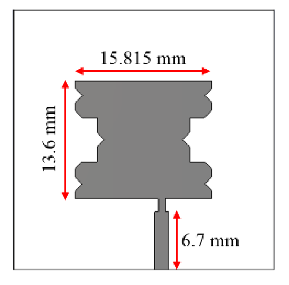
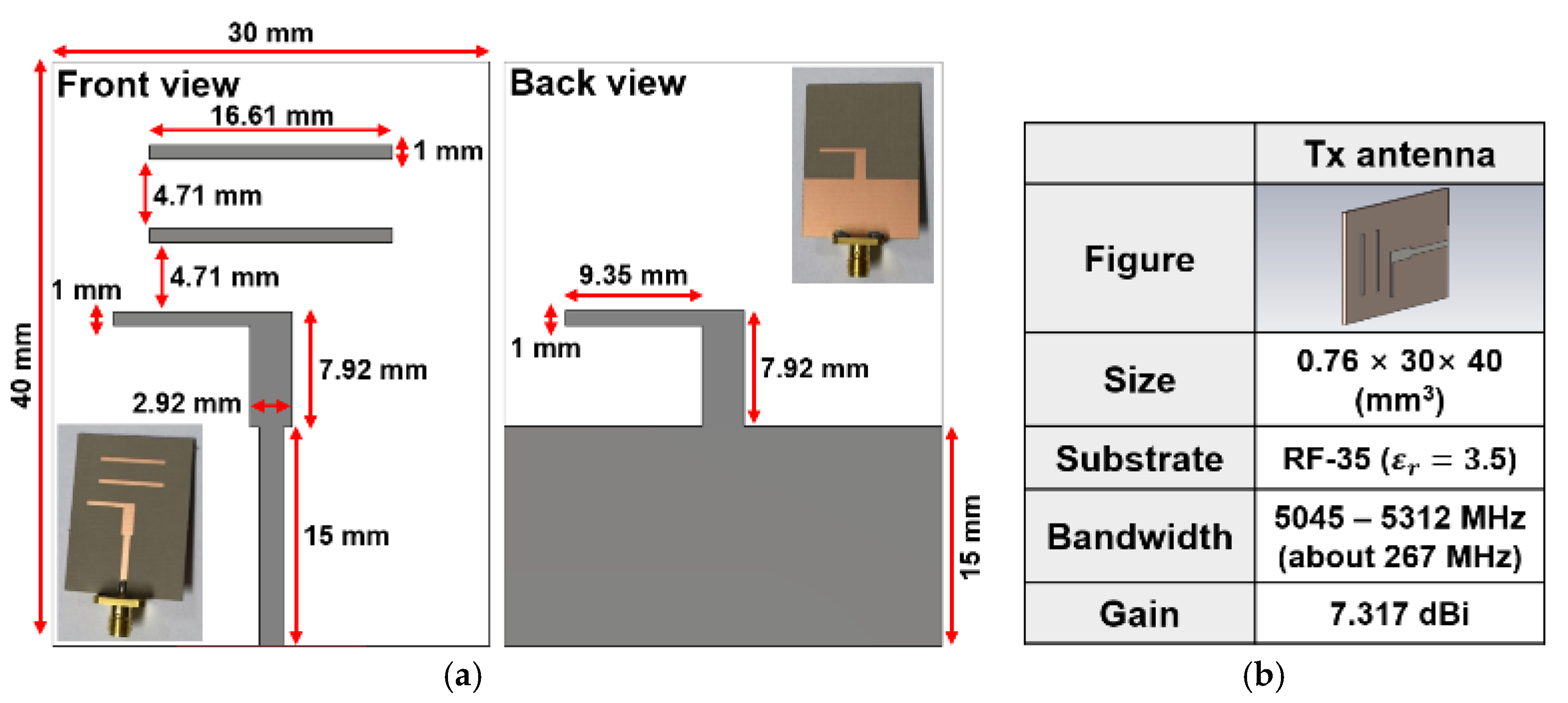
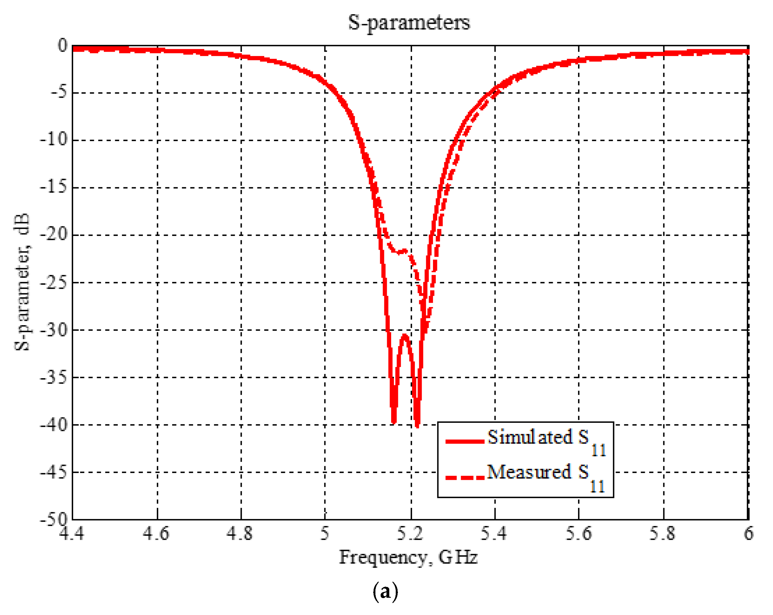
2.3. Tx and Rx Antenna Design

The antenna takes the RF signal (5.2 GHz) from the Tx power amplifier and feeds it to the EH system and memory cell. A Koch fractal patch antenna with high reflection co-efficiency and gain and an inter-element spacing equal to 0.5λ (at the design frequency of 5.2 GHz, λ is the wavelength in free space) as a compact size for the Rx module side is implemented as shown in Figure 6.
Figure 7a,b illustrate a 5.2 GHz Quasi-Yagi antenna configuration on the substrate of Taconic RF-35 (0.76 mm) to transmit a total power of 3 W, being used as a wireless power transmitter and its specification.
An Rx module designed by a 2 × 3 array antenna is located at a distance up to around 1 m (the distance can vary to harvest more RF input power) from the transmitter to harvest the transmitted power as shown in Figure 8a. The broadside gain of each port Rx antenna is shown in Figure 8b.

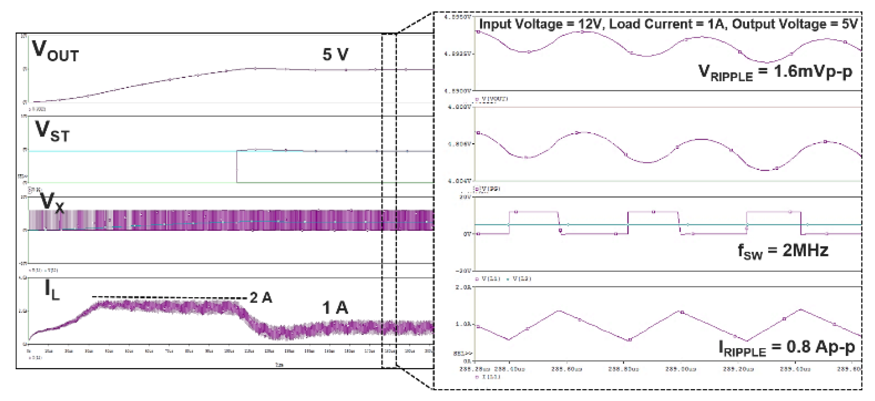
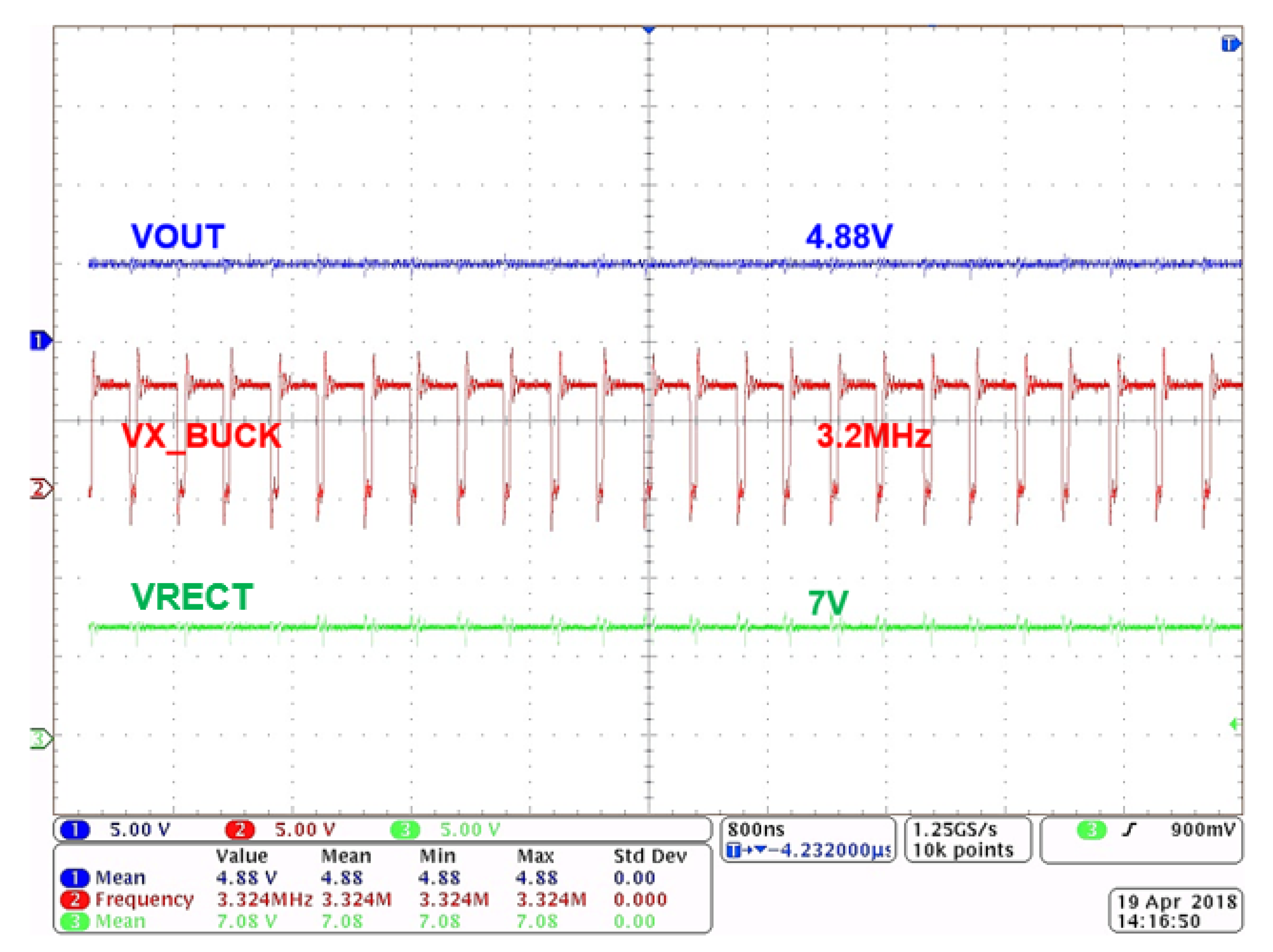
3. Implementation and Experimental Results

The module of the proposed RF EH including reconfigurable scheme and third harmonic control with the information of the PCB layers is shown in Figure 9a,b. The 6-parallel rectenna shows 67% conversion efficiency and higher than 6.1 V output DC voltage at the input power level of +20 dBm. 4% improvement in efficiency is achieved in compared with the case without the third harmonic control circuit and efficiency.
The presented RF-DC converter simultaneously provides both higher output DC voltage and conversion efficiency, and this results in a higher overall conversion efficiency and simpler system configuration of the whole RF EH system. Figure 10a–c show measurement environments of RF EH systems. During the measurement in two setups, a 5.2 GHz RF signal via the power amplifier and Tx antenna is transmitted, which charges the wearable device, chip Light Emitting Diode (LED), mobile phone, and LG products at respective distances of 65 cm, 80 cm, 90 cm, and 25 cm, with a transmission power of 34.77 dBm for the wearable device, chip LED, and mobile phone and 30 dBm for LG products. Figure 11a,b show the measured reflection coefficient (S11) of Tx antenna and Rx antennas, respectively. The −10 dB reflection bandwidth of the designed Tx antenna is 7.4% (5.08‒5.32 GHz). The measurement results for power conversion efficiency of the RF EH system are illustrated in Figure 12. The rectenna provides a maximum 6.1 V output DC voltage in the frequency band of over 5 GHz, and high conversion efficiency is also observed. By increasing the number of involved parallel stages, efficiency at higher input power levels is high (diode operation in the breakdown area at high power is dominant in decreasing the efficiency). The maximum achieved efficiency at the +20 dBm input power level is 67% when a single rectenna is used. The test-bench has been configured for a 12 V input and 5 V output at 1 A load.
The simulation result of the buck-boost converter is illustrated in Figure 13. The maximum efficiency of the buck-boost converter reaches 93% at 2 MHz switching frequency. The measured functional performance of the RF EH harvester system is illustrated in Figure 14. Table 2 lists the important metrics of the RF RH system including key features, elements used in the Rx module, and PCB boards. Table 3 summaries the whole performance of the RF EH. During the measurement, the USB connector is connected to IoT/wearable devices such as a G watch, LED, and cell phone.

4. Conclusions

In this paper, an RF energy harvester based on a reconfigurable and multiple parallel rectenna with third harmonic control at the frequency band of 5.2 GHz was presented. In the proposed scheme, RF-DC conversion using a 6-parallel rectenna is realized. This approach provided high efficiency and output DC voltage level, which allowed the use of a simple buck DC-DC converter after the RF-DC converter. Finally, the buck DC-DC converter fixed the output voltage and supplied the IoT device or BLE chip. The presented architecture achieved maximum 67% power conversion efficiency and 6.1 V DC voltage at the input power level of +20 dBm. Using the proposed architecture, higher and different values of DC output voltage and power conversion efficiency can be obtained. Therefore, it can be used to power-up various IoT/wearable devices.

Author Contributions

H.A. designed and performed experiments, analyzed the data, and wrote the manuscript. A.H., B.S.R., S.Y.K., J.B., J.M.L., J.H.M., J.J.P., and Y.G.P. conceived and planned the simulation and measurements. A.H., B.S.R., S.Y.K., and Y.G.P. contributed to the design and implementation of the research, to the analysis of the results, and to the writing of the manuscript. K.C.H., Y.Y., D.I.K., and K.-Y.L. devised the project, the main conceptual ideas, and proof outline. K.-Y.L. supervised the project. All authors have read and agreed to the published version of the manuscript.

Funding

This research received no external funding.

Acknowledgments

This work was supported by the National Research Foundation of Korea (NRF) grant funded by the Korean government (MSIP) (2014R1A5A1011478).

Conflicts of Interest

The authors declare no conflict of interest.

References

  1. Suh, Y.H.; Chang, K. A high-efficiency dual-frequency rectenna for 2.45- and 5.8-GHz wireless power transmission. IEEE Trans. Microw. Theory Tech. 2002, 50, 1784–1789. [Google Scholar] [CrossRef] [Green Version]
  2. Nishida, K.; Taniguchi, Y.; Kawakami, K.; Homma, Y.; Mizutani, H.; Miyazaki, M.; Ikematsu, H.; Shinohara, N. 5.8 GHz high sensitivity rectenna array. In Proceedings of the 2011 IEEE MTT-S International Microwave Workshop Series on Innovative Wireless Power Transmission: Technologies, Systems, and Applications, Kyoto, Japan, 12–13 May 2011; pp. 19–22. [Google Scholar]
  3. Tu, W.; Hsu, S.; Chang, K. Compact 5.8-GHz rectenna using stepped-impedance dipole antenna. IEEE Antennas Wirel. Propag. Lett. 2007, 6, 282–284. [Google Scholar] [CrossRef]
  4. Chin, C.; Xue, Q.; Chan, C. Design of a 5.8-GHz rectenna incorporating a new patch antenna. IEEE Antennas Wirel. Propag. Lett. 2005, 4, 175–178. [Google Scholar] [CrossRef]
  5. McSpadden, J.; Fan, L.; Chang, K. Design and experiments of a high-conversion-efficiency 5.8-GHz rectenna. IEEE Trans. Microw. Theory Technol. 1998, 46, 2053–2060. [Google Scholar] [CrossRef]
  6. Furukawa, M.; Takahashi, Y.; Fujiwara, T.; Mihara, S.; Saito, T.; Kobayashi, Y.; Kawasaki, S.; Shinohara, N.; Fujino, Y.; Tanaka, K.; et al. 5.8-GHz planar hybrid rectenna for wireless powered applications. In Proceedings of the 2006 Asia-Pacific Microwave Conference, Yokohama, Japan, 12–15 December 2006; pp. 1611–1614. [Google Scholar]
  7. Yi, H.; Yu, W.H.; Mak, P.I.; Yin, J.; Martins, R.P. A 0.18-V 382-μW Bluetooth Low-Energy Receiver Front-End With 1.33-nW Sleep Power for Energy-Harvesting Applications in 28-nm CMOS. IEEE J. Solid-State Circuits 2018, 53, 1618–1627. [Google Scholar] [CrossRef]
  8. Abbasizadeh, H.; Kim, S.Y.; Nga, T.T.K.; Khan, D.; Oh, S.J.; Kim, S.J.; Lee, K.Y. A 5.2 GHz RF Energy Harvester System Using Reconfigurable Parallel Rectenna. In Proceedings of the 2018 IEEE 61st International Midwest Symposium on Circuits and Systems (MWSCAS), Windsor, ON, Canada, 5–8 August 2018; pp. 436–439. [Google Scholar]
  9. Wireless Powered Sensor Networks (WPSN) Testbed. Available online: https://youtu.be/qP9fZQX1sDk (accessed on 20 December 2019).
  10. Moon, J.H.; Park, J.J.; Kim, D.I. New Reconfigurable Nonlinear Energy Harvester: Boosting Rate-Energy Tradeoff. In Proceedings of the 2018 IEEE 87th Vehicular Technology Conference (VTC Spring), Porto, Portugal, 3–6 June 2018. [Google Scholar]
  11. Boaventura, A.S.; Carvalho, N.B. Maximizing DC power in energy harvesting circuits using multisine excitation. In Proceedings of the 2011 IEEE MTT-S International Microwave Symposium Digest (MTT), Baltimore, MD, USA, 5–10 June 2011; pp. 1–4. [Google Scholar]
  12. Clerckx, B.; Bayguzina, E. Waveform Design for Wireless Power Transfer. IEEE Trans. Signal Process. 2016, 64, 6313–6328. [Google Scholar] [CrossRef] [Green Version]
  13. Boshkovska, E.; Ng, D.W.K.; Zlatanov, N.; Schober, R. Practical nonlinear energy harvesting model and resource allocation for SWIPT systems. IEEE Commun. Lett. 2015, 19, 2082–2085. [Google Scholar] [CrossRef]
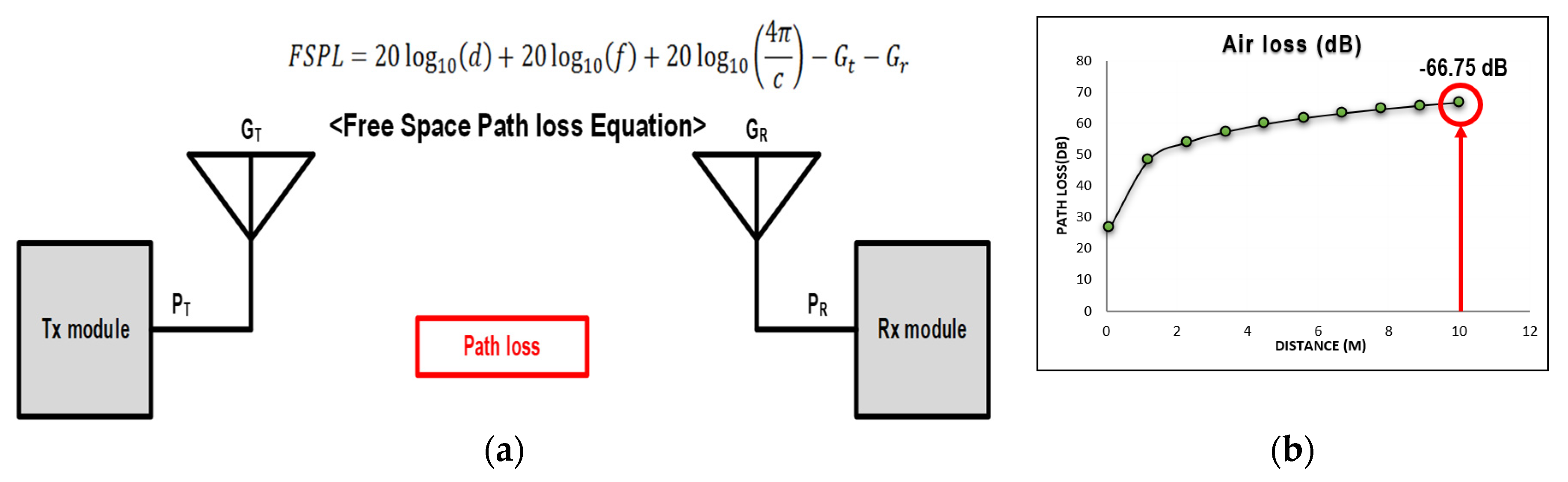
 [Green Version]
Figure 1. Top block diagram of the radio frequency (RF) energy harvester. Reprint with permission [4775431338148]; 2020, IEEE.
Energies 13 01023 g001
Figure 2. (a) System budget and (b) path loss measurement vs. distance. Reprint with permission [4775431338148]; 2020, IEEE.
Energies 13 01023 g002
Figure 3. The proposed RF energy harvester system block diagram. Reprint with permission [4775431338148]; 2020, IEEE.
Energies 13 01023 g003
Figure 4. (a) The proposed rectenna structure and (b) Its parallel configuration. Reprint with permission [4775431338148]; 2020, IEEE.
Energies 13 01023 g004
Figure 5. Non-linear PCE curve characteristics of the single-stage rectenna.
Energies 13 01023 g005
Figure 6. Koch fractal patch antenna. Reprint with permission [4775431338148]; 2020, IEEE.
Energies 13 01023 g006
Figure 7. Configuration of the designed quasi-Yagi Tx antenna, (a) Front and back sides, (b) Specifications of the Tx antenna. Reprint with permission [4775431338148]; 2020, IEEE.
Energies 13 01023 g007
Figure 8. (a) 2 × 3 Rx module antenna arrangement and (b) Specifications. Reprint with permission [4775431338148]; 2020, IEEE.
Energies 13 01023 g008
Figure 9. (a) Module of the fabricated RF RH, front (6-parallel rectenna) and back (Rx receiver) sides and (b) Information of the PCB layer (4 layers). Reprint with permission [4775431338148]; 2020, IEEE.
Energies 13 01023 g009
Figure 10. Test environment of the proposed RF EH (a) The Rx receiver board is connected to a G watch, (b) Chip LED, and (c) Mobile phone. Reprint with permission [4775431338148]; 2020, IEEE.
Energies 13 01023 g010
Figure 11. Reflection coefficient of (a) the Tx antenna and (b) 2 × 3 Rx antenna.
Energies 13 01023 g011aEnergies 13 01023 g011b
Figure 12. Measured efficiency vs. input power level of the proposed RF EH system (a) Different number of parallel rectenna stages and (b) Output voltages. Reprint with permission [4775431338148]; 2020, IEEE.
Energies 13 01023 g012
Figure 13. Simulation results of the buck-boost DC-DC converter. Reprint with permission [4775431338148]; 2020, IEEE.
Energies 13 01023 g013
Figure 14. Measured results of the RF EH harvester.
Energies 13 01023 g014
Table 1. System Budget. Reprint with permission [4775431338148]; 2020, IEEE.
Distance
(m)
Output   Power   ( P T )
(dBm)
Transmitter   Antenna   Gain   ( G T )
(dBi)
Receiver   Antenna   Gain   ( G R )
(dBi)
Path Loss
(dB)
Received Power
(dBm)
10487.31713 (6 array rectenna)−66.750.967
5−60.736.987
1−46.7521.067
Table 2. Performance Summary. Reprint with permission [4775431338148]; 2020, IEEE.
ParameterTest Board
RF-DC converter type6-parallel rectenna
Key features1. Diode reliability considered
2. Parallel rectenna structure
3. Reconfigurable structure
4. Implementation for large input power
DiodeAVAGO HSMS-2862
Buck-boost converterTI TPS63060
PCB board typeTaconic RF35 (Front: EH system)
+ FR4 (Back: BLE, DC-DC converter)
Peak efficiency67% @20 dBm, 5.2 GHz
Table 3. Performance Summary of IoT/wearable Devices. Reprint with permission [4775431338148]; 2020, IEEE.
ParameterLG G Watch
(Wearable Device)
Mi Band
(Wearable Device)
LG SmartThinQ
(IoT, Sensor)
Battery capacity400 mAh, 1.52 Wh45 mAh, 0.17 Wh300 mAh, 1.11 Wh
Battery Life a24 h30 day90 day
Power Consumption63 mW0.24 mW0.51 mW
Distance25 cm25 cm25 cm
Transmission Power30 dBm30 dBm30 dBm
Antenna Gain20 dBi20 dBi20 dBi
Free Space Path Loss−33.69 dB−33.69 dB−33.69 dB
Received Power16.31 dBm16.31 dBm16.31 dBm
Battery charging time buse time increased by 158%8 h36 h
Duration and use time aspectsuse time increased by 158%Continuous use without battery reduction when Tx Power is suppliedContinuous use without battery reduction when Tx Power is supplied
a Battery Life = (Battery capacity [Wh]/Power Consumption [W]). b Battery charging time = (Battery capacity [mAh]/Charger output current [mA]) × Charging factor (1.2).

