Article

Composite Sinusoidal Waveform Generated by Direct Digital Synthesis for Healthy Charging of Lithium-Ion Batteries

1
Center for Condensed Matter Sciences, National Taiwan University, Taipei 10617, Taiwan
2
Department of Chemical Engineering and Biotechnology, National Taipei University of Technology, Taipei 10608, Taiwan
3
Department of Vehicle Engineering, National Taipei University of Technology, Taipei 10608, Taiwan
4
Department of Mechanical Engineering, National Pingtung University of Science and Technology, Pingtung 91201, Taiwan
*
Authors to whom correspondence should be addressed.
These authors contributed equally.
Energies 2020, 13(4), 814; https://doi.org/10.3390/en13040814
Submission received: 10 January 2020 / Revised: 2 February 2020 / Accepted: 12 February 2020 / Published: 13 February 2020
(This article belongs to the Section D: Energy Storage and Application)

Abstract

:
To address the defects in lithium-ion battery lifespan, this paper proposes a composite waveform generation strategy that offers capacity-recovering effect. Based on digital architecture, this study exploits direct digital synthesis (DDS) to generate data, which are then processed in an analog-to-digital converter to produce a predefined voltage waveform signal. In the process, an arbitrary waveform is converted to digital voltage waveform signal through pulse width modulation (PWM) technology, thus realizing waveform generation through DDS. Subsequently, analog-to-digital conversion is accomplished by going through a buck circuit, resulting in a composite sinusoidal waveform that is used to charge the battery with a recovering effect. This paper comprises an introduction of effective waveforms for capacity recovering, methods of generating composite sinusoidal waveforms, and an example of the application of composite sinusoidal waveform generation. The waveform produced by the circuit may recover the capacity of an aged 18650 lithium-ion battery by about 8%.

1. Introduction

With the global rise of environmental awareness, electric vehicles have become the most important technological–development objective for governments and enterprises. Among them, the most developed are the electric vehicles with lithium-ion batteries as the power source. The current technology has been used to design lithium-ion electric vehicles that function as similarly as possible to petrol vehicles that consumers drive. However, lithium-ion battery electric vehicles have not been able to replace fuel cars on a large scale thus far, chiefly owing to issues such as limited longevity and long charging time [1]. Many studies have concluded that the most prominent cause of lithium-ion battery aging is that during charging, molecules of the electrolyte combine with the lithium atoms to form a passivation layer of solid electrolyte interface (SEI), which leads to depleted recyclable lithium ions in the electrolyte and a subsequent decline in battery capacity [2,3]. Constant current/constant voltage (CC/CV) charging is the most commonly used method for charging lithium-ion batteries today. The CC/CV charging involves charging a battery at a CC until its voltage reaches the predetermined limit, followed by CV charging until the current decreases to a predetermined low value. However, SEI formation occurs near the end of the CC-charging step during normal CC/CV charging if the charging current rate reaches or exceeds a certain value. In the condition of high C-rate charging of electric vehicles, battery capacity is more likely to decline, leading to aging of the battery, decrease in battery cycle life, and decrease in rated service life [4,5]. It also leads to a high cost of maintenance and the replacement of battery pack, as well as difficulty in cost reduction, hindering the wide application of electric vehicles [6]. Therefore, to mitigate the SEI passivation issue with CC/CV charging, other charging methods have been proposed, such as pulse charging [7], Motorola charging [8], reflex charging [9], and sinusoidal waveform charging [10].
The recently proposed composite sinusoidal waveform charging has the greatest potential for further development as it can avoid unnecessary energy wastage and avoid the aging due to SEI formation. For example, when using ethylene carbonate (EC) as an electrolyte, the reaction started with chemical reduction reaction that lead to the formation of a LiOCO2C2H4 radical. LiOCO2C2H4 radicals can extensively react to form solid molecules and stack onto the graphite negative electrode. The reduction reaction occurs in the succession of electron transfer to the Li-EC during charging. An improper charging method via constantly pumping electronic energy into the battery may enhance the reaction. The ceaseless reaction during the charge/discharge cycle is the key significant aging problems of Li-ion batteries. Therefore, first-principle calculations were applied to evaluate the positive voltage required for the lithium ions to migrate from the positive electrode to the negative during charging [11]. Moreover, a small section of negative voltage is incorporated that can reverse reduction reaction on the negative electrode during charging. Such combination forms a novel strategy of composite sinusoidal waveform charging. We have utilized the instrument (N6785A, Keysight Technologies, Inc., Santa Rosa, CA, USA) to generate the composite sinusoidal waveform. By using a voltage waveform format, we conducted experiments on the 18650 lithium-ion battery charged via a large current of 3.45 C. Compared with the CC/CV method, we verified that this charging method can increase the battery capacity of an aged 18650 Li-ion battery by 18.7%, reduce maximum temperature rise by 9 °C, and reduce charging time by 25 min [12].
The composite sinusoidal waveform can avoid unnecessary energy wastage, delay battery aging, and even recover battery capacity. In our preliminary verifications [11,12], we have used commercially available chargers to generate the waveforms for charging. However, to meet the broadening requirements of charging in the future [13,14,15], it is certainly necessary to develop a device for the generation of composite waveform. Both analog and digital architects can generate a voltage waveform signal. However, when an analog architect is applied, oscillator hardware is used to generate the voltage waveform signal. Although the method is rapid, it has the disadvantages of limited frequency precision, low stability, low resolution, and parameter settings, rendering it unfavorable for computer program control. Furthermore, parameters such as amplitude and frequency should be allowed to be adjusted to adapt to various types of batteries that may require different shape of waveforms [11]. The utilization of direct digital synthesis (DDS) [16] provides another suitable method. DDS rapidly reads a series of digital waveform data from the waveform register through the phase accumulator. The data are then processed in an analog-to-digital converter to produce a predefined voltage waveform signal. It does not require oscillator hardware components; further, it possesses advantages such as higher precision, stability, resolution, and bandwidth, as well as the ability to tune the frequency in continuous phase. Therefore, this study is based on the digital architecture. We developed a composite waveform circuit with the effects of reviving and prolonging cell life.

2. Methods

The voltage amplitude and frequency of the charging strategy in this paper follow those from the theoretical model in [11]. The waveform is shown in Figure 1a. We have already verified and demonstrated that this composite sinusoidal waveform is effective in prolonging the 18650 lithium-ion battery life [12]. The waveform has voltage level of 3.6 V. The upper cycle and lower cycle are 0.7 V and 0.2 V, respectively. The frequency is 1 kHz. As the cell voltage reaches the full voltage, the lower cycle of the waveform can discharge the battery. The circuit we developed can generate such a waveform. Figure 1b shows the roadmap that the circuit comprises three parts. The first part is a pulse width modulation (PWM) for generating a digital signal of the composite sinusoidal waveform. The second part is to amplify the digital signal to the power level. The third part is a low-pass filter circuit that converts the digital signal into a voltage waveform for effective battery charging. In addition, we reserved a signal feedback function in the program [17,18], such that the circuit can provide the appropriate charging waveform in real time by incorporating databases and artificial intelligence (AI) decisions in the future. The microchip dsPIC30f4011 digital signal processor (DSP; Microchip Technology Inc., Chandler, AZ, USA) [19] with high computing speed and low delay time was selected as the important component of composite waveform generation to allow the frequency of the output waveform to be above 1 kHz to avoid the impact of resolution on the waveform, and to reduce slowing down of Microcontroller Unit (MCU) processing by analog-to-digital reading. The charging circuit design adopts the buck circuit architecture, with TLP250 selected as the inner gate driver. In addition to driving MOSFET, it also isolates the signal from the power level. Metal-Oxide-Semiconductor Field-Effect Transistor (MOSFET) adopts the P-type IRF9540N and N-type IRF3705. Subsequently, restoration of the composite waveform is achieved by an LC low-pass filter.

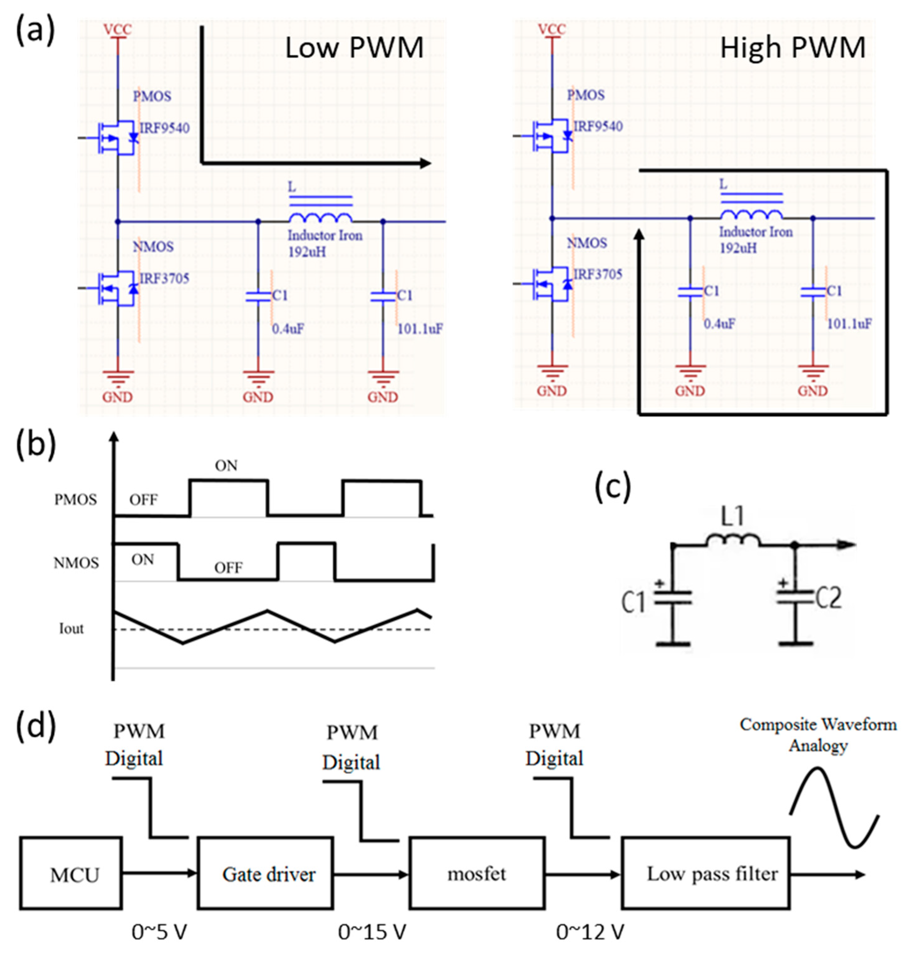
2.1. Direct Digital Synthesis (DDS) and Buck Converter

In the first part of signal generation, the structure of DDS comprises the phase accumulator, waveform memory, analog-to-digital converter, and low-pass filter, as shown in Figure 2a. The phase accumulator, which is the most important in the DDS module, comprises the N-bit adder and N-bit accumulator register. The principle of its operation is as follows. With an incoming reference frequency f clk , the accumulator accumulates the frequency control FW with the output value of the register ( f out ), the result of which is then input to the register. The accumulator register feeds the data generated in the previous reference clock into the accumulator by way of feedback. Under the action of the clock, the frequency control can be constantly accumulated. In the meantime, by using the data output from the phase accumulator as the address, the amplitude table corresponding to the said address is found in the waveform memory. The transformation from phase to amplitude is thus accomplished. The equation for computing the output frequency is as follows:
f o u t = f c l k 2 N F W .
The equation for computing the resolution of output signal frequency ( f ) is as follows:
f = f c l k 2 N .
A stable average output voltage is generated as the buck converter adjusts the duty cycle and switches the ON/OFF status of the circuit, which passes through an LC filter, as shown in Figure 2b. The working timing of the converter is shown in Figure 2c. When the MOSFET is ON in the working time, the current is transmitted to the load end through the inductor, which also accumulates energy. Meanwhile, the diode state is OFF. When the MOSFET is OFF, the energy accumulated in the inductor is supplied to the load end as a current flow through the diode [20,21,22,23].
Based on the voltage and current stress analysis, the maximum current I L m a x through the inductor L is that given by Equation (3), where R L d is the load resistance, i L is filter inductance, I o is the load current, D y is the duty cycle, and T s is the switching period.
I L m a x = I o + 1 2 i L = V o u t R L d [ 1 + R L d 2 L ( 1 D y ) T s ]
The rated voltage V V T of the switch MOSFET and flyback diode V V D is given by Equation (4), where V V T is the rated voltage at the switch MOSFET and V V D is the rated voltage at the flyback diode.
V V T = V V D = ( 2 ~ 3 ) V i n
The rated current I V T of the switch MOSFET and flyback diode I V D is given by
I V T = I V D = ( 1.5 ~ 2 ) I L m a x
The filter inductance i L is computed by Equation (6). When D y = 0.5 , L is at its maximum
i L = V i n V o L D y T s = V i n ( 1 D y ) L D y T s
L = V i n ( 1 D y ) D y T s i L .
Computing the filter capacitor, where f s is the switch frequency, the charge of capacitor C in one switching cycle is
Q = 1 2 i L 2 T s 2 = i L 8 f s .
The output ripple voltage V O is evaluated by
V O = Q C = ( 1 D y ) V O 8 L C f s 2 .
The filter capacitance C is
C = ( 1 D y ) V O 8 L f s 2 V O .

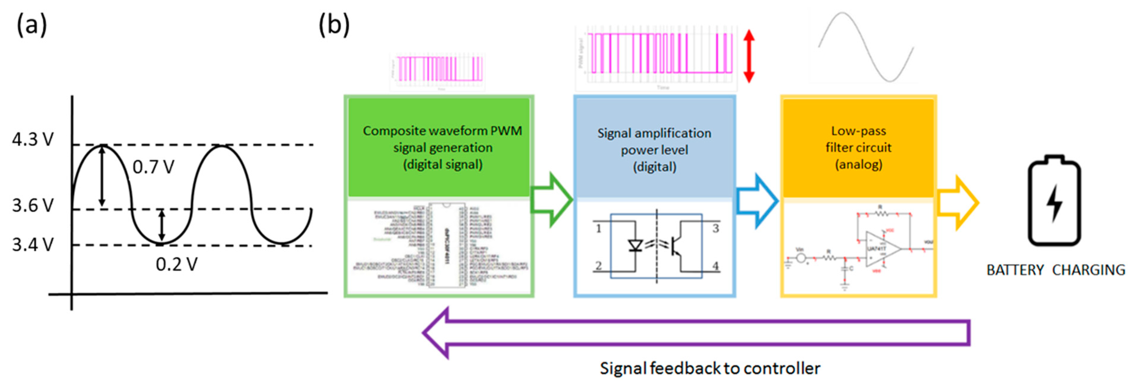
2.2. Waveform Generation

To generate a composite waveform that is effective for capacity recovery, dsPIC30f4011 chips are first used in conjunction with DDS. Interpolation is used to convert the composite waveform into program codes. The designed LC low-pass filter is used to verify the waveform. The cycle of correction, fine tuning, and verification is launched when there is discrepancy between the generated waveform and the target waveform. The composite waveform development process is completed only when the generated waveform agrees with the target waveform.
Primary Master Time Base Period Register (PTPER) is defined as the primary parameter for the development of composite waveform. Its purpose is to set the upper limit of the frequency and resolution of the composite waveform. The time-base module required to generate a PWM signal in dsPIC30f4011 chip can be categorized into four working modes: free running mode, single event mode, continuous up/down counting mode, and continuous up/down mode with interrupts for double-updates. In this study, all PWM outputs adopt the continuous up/down counting mode. To strike a balance between frequency and resolution, this study takes a prioritized resolution directive and sets the maximum output voltage (Vmax) of the chip at 5 V and the register precision (Vacc) at 100 mV per grid. Based on the calculation via the resolution equation, the resolution of the register at 100 mV per grid is obtained when PTPER is 25. In addition to meeting the requirements of the composite waveform, it also ensures high PWM output frequency, such that the composite waveform output can be above 1 kHz.
The conversion between the composite waveform generated and the registered value in the program code is achieved by computing the PWM duty cycle of 0–100% in the established composite waveform via Equation (11), then comparing with the values read from PDCx register. PDCx is the ratio of duty cycle of the PWM output. PTPER << 1 represents moving the binary value one bit to the left, corresponding to a multiplication by two in the decimal system.
Duty cycle = PDCx/(PTPER << 1) × 100%
Through the conversion of values in the register, the corresponding values read from the PDCx register can be known for every width of PWM duty cycle. The following paragraphs explain how the conversion is achieved from analog voltage signals to digital PWM duty cycle values. Adjustment is made to the voltage level, the first parameter of the voltage waveform. Then, the second and third parameters are adjusted, which are the upper/lower half-cycle amplitudes and waveform frequency, respectively. Finally, the three parameters are fine-tuned into a one-line program instruction to simplify program complexity and to improve readability. All the above output signals are the PWM value, which are difficult to read and to verify whether they are consistent with the target. Therefore, the low-pass filter is designed and implemented to verify whether the various parameter settings meet the target value.
To verify conformance of the PWM signal to the target voltage waveform, it is necessary to restore the PWM digital signal to a continuous analog waveform signal through the low-pass filter to improve the visibility [24]. The lower filter circuit adopts an LC low-pass filter with wide applicability and good stability [25,26]. The frequency of the target composite waveform is the cut-off frequency of the low-pass filter that is set to about 1 kHz. The designing method is such that common L and C levels are substituted into the lower cut-off frequency to carry out theoretical calculations. The optimal values for filter L and C are found through repeatedly applied verifications. To verify the design of the PWM low-pass filter circuit, an exemplary sinusoidal PWM value is first selected as the basis for LC adjustment of the filter. It is found through verification that the best filter is one with an L of 12.5 mH and C of 1 μF. The cut-off frequency of the low-pass filter is reversely deduced via the equation to be 1.42 kHz, which is close to the original ideal value of 1 kHz.
Voltage values are converted to code parameters by taking advantage of the characteristic of linear interpolation, i.e., any two adjacent tabular points can be connected by a straight line. All the values of a therein can be correlated to a linear function b(x). Taking advantage of the feature that a straight line has a constant slope, the following relation can be expressed as Equation (12) [27,28]:
(bb1)/(aa1) = (b2b1)/(a2a1).
The target of this study is defined in such a manner that the upper and lower half-cycles are separate, thus, a1 and b1 in the equation can be assumed as 0. Consequently, a is assumed to be the maximum of sine(a), which is 1, and b is assumed to be a varied value of sine(a). Correspondingly, a2 in the equation is the maximum width of the PWM at 100% of the duty cycle. This value is fixed at 50 throughout the present study, half the value of the entire maximum amplitude. This value is also related to the PTPER value. The variable b2 is the PDC1 value to be obtained by this study, whose value varies with b.
The HIGH of the PWM signal output by MCU is the actual voltage of 5 V. Therefore, based on Equation (12), 5 can be substituted into a; b is the target amplitude voltage of 3.6 V; a2 is 50, the maximum value of the matrix; b2 is hence the value of the PDCx register to be obtained. It is assumed here that a1 and b1 are 0. By calculation, the target composite waveform voltage level of 3.6 V corresponds to a PDCx value where b2 equals 36. After passing through the filter, the output is 3.36 V, which deviates from the target value of 3.6 V. Repeated corrections by experiment yielded a PDCx value of 38, at which point the output voltage target can be achieved after passing through the filter.
Through the abovementioned interpolation method, the parameters of the sinusoidal wave matrix with the maximum amplitude can be obtained. The next step is to interpolate the value of PDCx register and the actual voltage output to find the required amplitude. The HIGH of the PWM signal output by MCU is the actual voltage of 5 V. Taking the upper half-cycle of 0.7 V as an example, through Equation (12), substituting 5 into a and the amplitude of the upper half-cycle 0.7 V into b, a2 is the maximum value of the matrix 50. The converted value to be obtained is b2, which equals 7. Taking the lower half-cycle of 0.2 V as an example, through Equation (12), substituting −5 into a and the amplitude of the lower half-cycle −0.2 V into b, a2 is then the maximum value of the matrix at −50. The converted value to be obtained is b2 equals −2.
After the abovementioned adjustments to the amplitude and the level, an important variable count has to be performed for the sequence of values to be concatenated into a continuous waveform output. In the program, after each output of the PWM waveform, 1 is added to the variable index to allow the MCU to read the next PWM value of the waveform matrix. As such, a continuous waveform output can be achieved. Therefore, after each PWM waveform output, when a value larger than 1 is added to the variable the number of waveforms in the same unit time will increase. However, this requires a balance between resolution and frequency. Increasing the variable indiscriminately after each PWM output will lead to the reduction of waveform resolution, which will eventually cause serious waveform distortion. Therefore, high analytical sampling is used in this study to mitigate the issue of resolution reduction when the frequency increases. Finally, the upper half-cycle value of PDCx equal to 7 and the lower half-cycle of PDCx equal to −2 are added to the computed voltage level PDCx register value of 38, the result of which is added to the program codes. This produces a waveform matrix that agrees with the target composite charging waveform in this study, as shown in Figure 1a.

2.3. Design of the Charging Circuit

The charging circuit is designed to adopt the form of a buck synchronous rectifier. A diode is connected after the switching element to allow the inductor to still be in a loop when the switching element is turned off to maintain a flowing current. This is to protect the switching element. Based on the principles of circuit operation, the circuit is set to switch on when the P-MOSFET is at LOW. The S pole of MOSFET is connected to the input power source. The D pole is connected to the power-storing inductor. When the LOW state is maintained at the G pole, MOS is open. When MOSFET is off, the energy in the inductor is released to the output end via the grounded diode. When the MCU output PWM is LOW, the top Positive Channel Metal Oxide Semiconductor (PMOS) is connected. In the meantime, the outer Vancouver Community College (VCC) supplies power to charge the inductor and capacitor. When MCU output PWM signal is HIGH, the top PMOS is disconnected. Then, the outer power is cut off. However, as a result of the afterflow from the inductor, PWM can filter out continuous composite waveforms, as shown in Figure 3a.
The working sequence is shown in Figure 3b. The charging loop filter is designed to adopt an LC π filter with low impedance input and output, as shown in Figure 3c. First, capacitor C1 removes most of the AC components. Then, the L1 and C2 filter are passed through. L1 presents a very high resistance to the AC component. Thus, the AC voltage drop over L1 is large, and the AC component supplied to the load is small. As for the DC component, because L1 does not exhibit inductive resistance, it is equivalent to an open circuit. Simultaneously, the filter inductor adopts a thick wire diameter with very small DC resistance. Therefore, no drop occurs for the DC voltage, resulting in relatively high DC output voltage. These are the main advantages of adopting an inductor filter. After repeated experimental designing as described above, we obtained the values for C1 to be 0.4 μF, L1 to be 192 μH, and C2 to be 101.1 μH. As the desired waveform output is in contrast to the stable DC output, which is the target of a buck architect, and the fixed duty cycle of the PWM is replaced by a variable in real-time PWM duty cycle signal. As verified by circuit simulation software, the composite waveform can be successfully generated.
Figure 3d shows the conversion of signals between components and the final output. The PWM signal of MCU has a fixed output of ca. 0–5 V. To drive the PMOS IRF5305, a higher voltage is needed to keep the PMOS operating in the saturation and cut-off regions. Driving the MOSFET with the HIGH output of only 5 V from the MCU presents a problem that needs to be addressed. In addition, to protect the MCU from being burned, the signal and the power level should be isolated. TLP250 is adopted for the gate driver to increase the PWM signal to ca. 0–15 V through a 15 V input from an external power supply, thereby driving MOSFET to operate in the saturation and cut-off regions. The output end is a battery which attenuates the input charging voltage waveform. Therefore, the VCC of PMOS is set to be larger than the composite waveform voltage. We adopt a 12 V power supply that is widely used in the market. Finally, PWM is restored to the composite waveform by LC low-pass filter in the buck circuit.

3. Result and Discussion

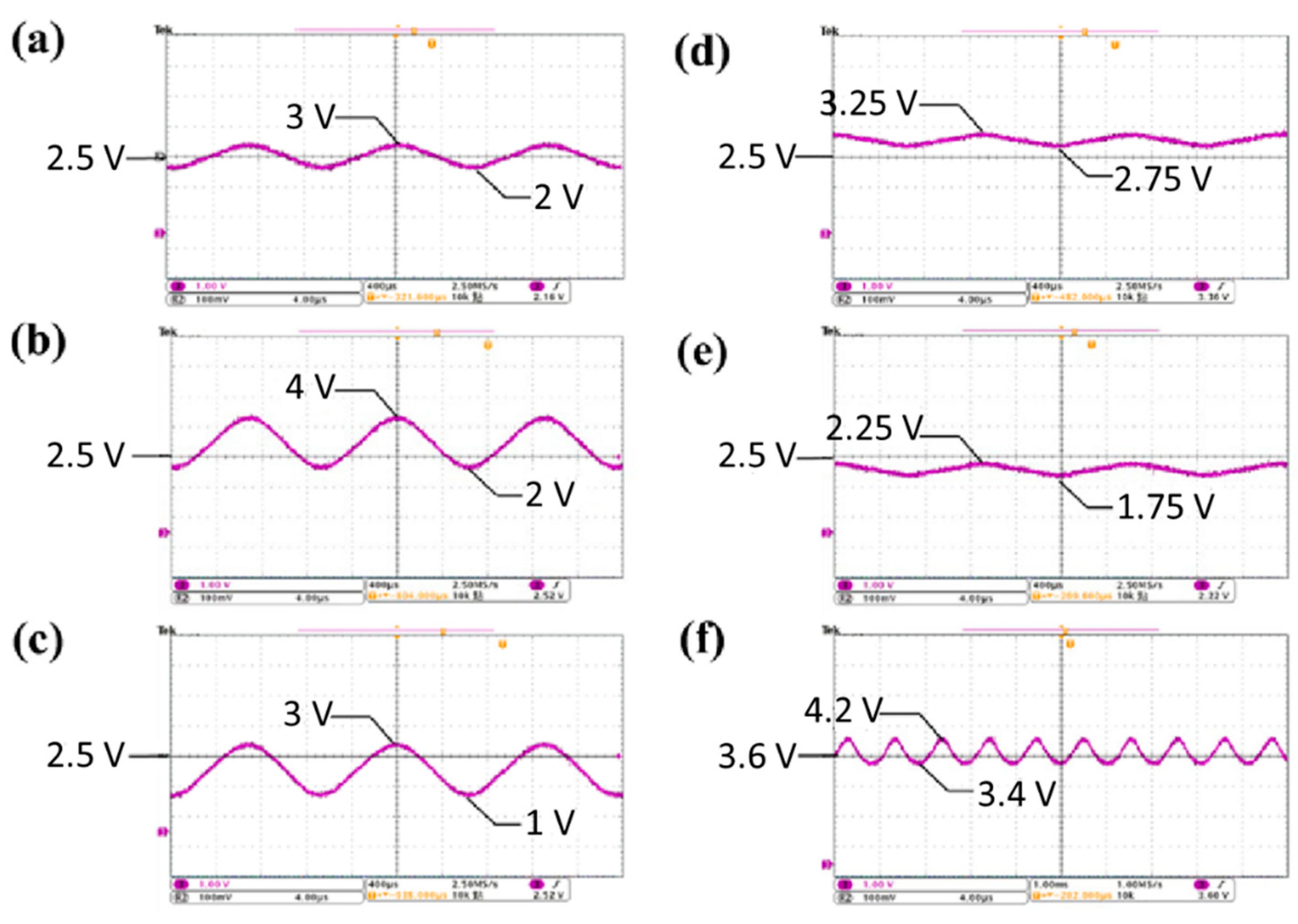
3.1. Verification of the Integrated Amplitude and Level Functions

The adjustments to the parameters of amplitude and level can be integrated into a series of equations to simplify the program coding. All composite waveforms can be generated by the four modes as follows. A represents the variable name of the waveform matrix. B is the matrix counting variable. C is the amplitude size adjustment variable. D is the adjustment variable of the level. Figure 4a below shows the verification of the developed composite waveform with 2.5 ± 0.5 V. Assume C to be equal to 2 and D to be equal to 10. The results of the verification are as follows. (i) With increased amplitude and level, PDCx = A[B] × C + D. The doubled amplitude V P P = 2 V and the level is increased by 0.5 V. This leads to the results shown in Figure 4b. (ii) With increased amplitude and decreased level, PDCx = A[B] × C − D. The doubled amplitude V P P = 2 V and the level decreased by 0.5 V. This leads to the results shown in Figure 4c. (iii) With decreased amplitude and increased level, PDCx = A[B]/C + D. The doubled amplitude V P P = 0.5 V and the level increased by 0.5 V. This leads to the results shown in Figure 4d. (4) With decreased amplitude and level, PDCx = A[B]/C–D. On the right is the doubled amplitude V P P = 0.5 V and level decreased by 0.5 V, resulting in that given by Figure 4e.
The target waveform takes reference from the optimized battery charging waveform described in [11], which ranged within 3.6 V. The waveform with an upper half-cycle of 0.7 V and lower half-cycle of 0.2 V is taken as the waveform for verification. By passing through the LC low-pass filter with L at 12.5 mH and C at 1 μF, as designed above, a waveform can be output as shown in Figure 4f.

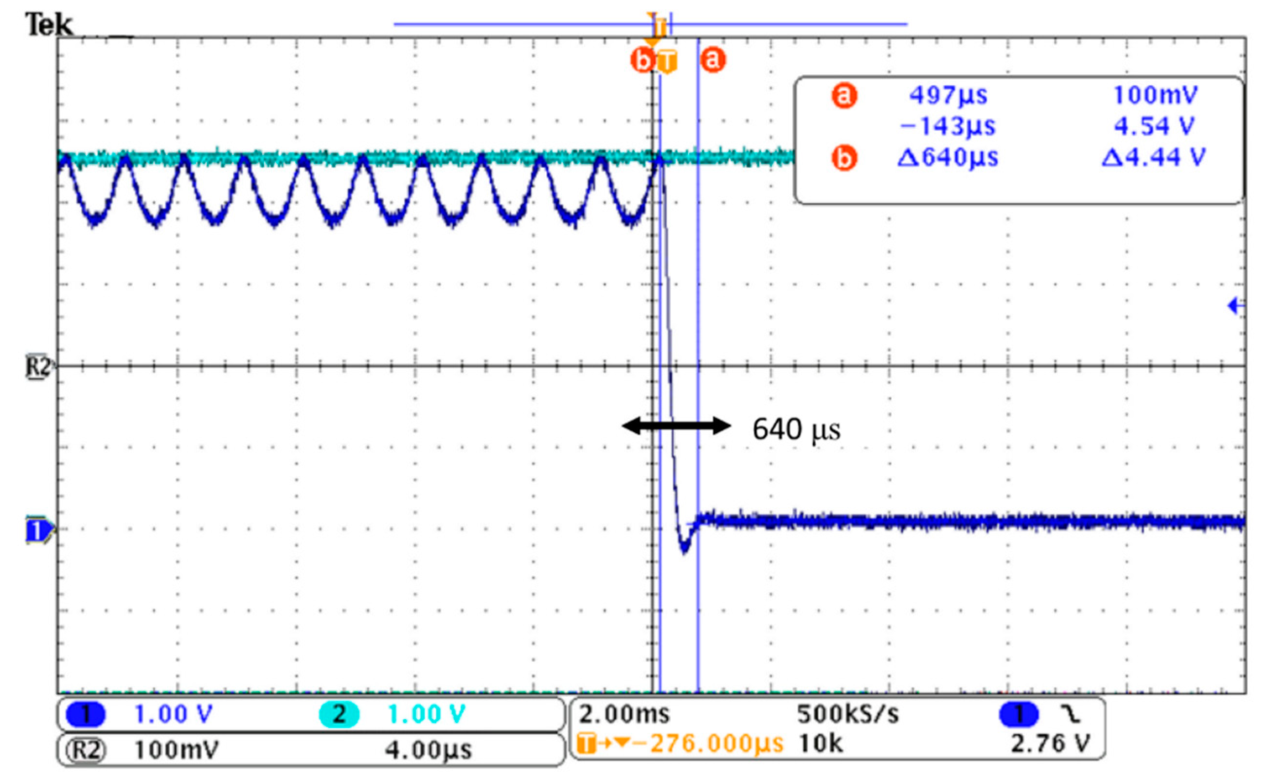
3.2. Verification of the Overvoltage Protection Function

This study predefines an average current less than 0.05 C as the condition of charge cut-off. When the above condition is met, the composite wave charging of the battery is completed. If the average current is not less than 0.05 C, then 1 is added to the PWM counter, and the output of the composite waveform to charge the battery continues. Figure 5 shows the required time in an applied operation. When the voltage is higher than 4.4 V, the microprocessor will instantly turn off the signal output with the turn-off time being 640 μs. Charging of the battery is suspended until the battery voltage returns to the normal criterion.

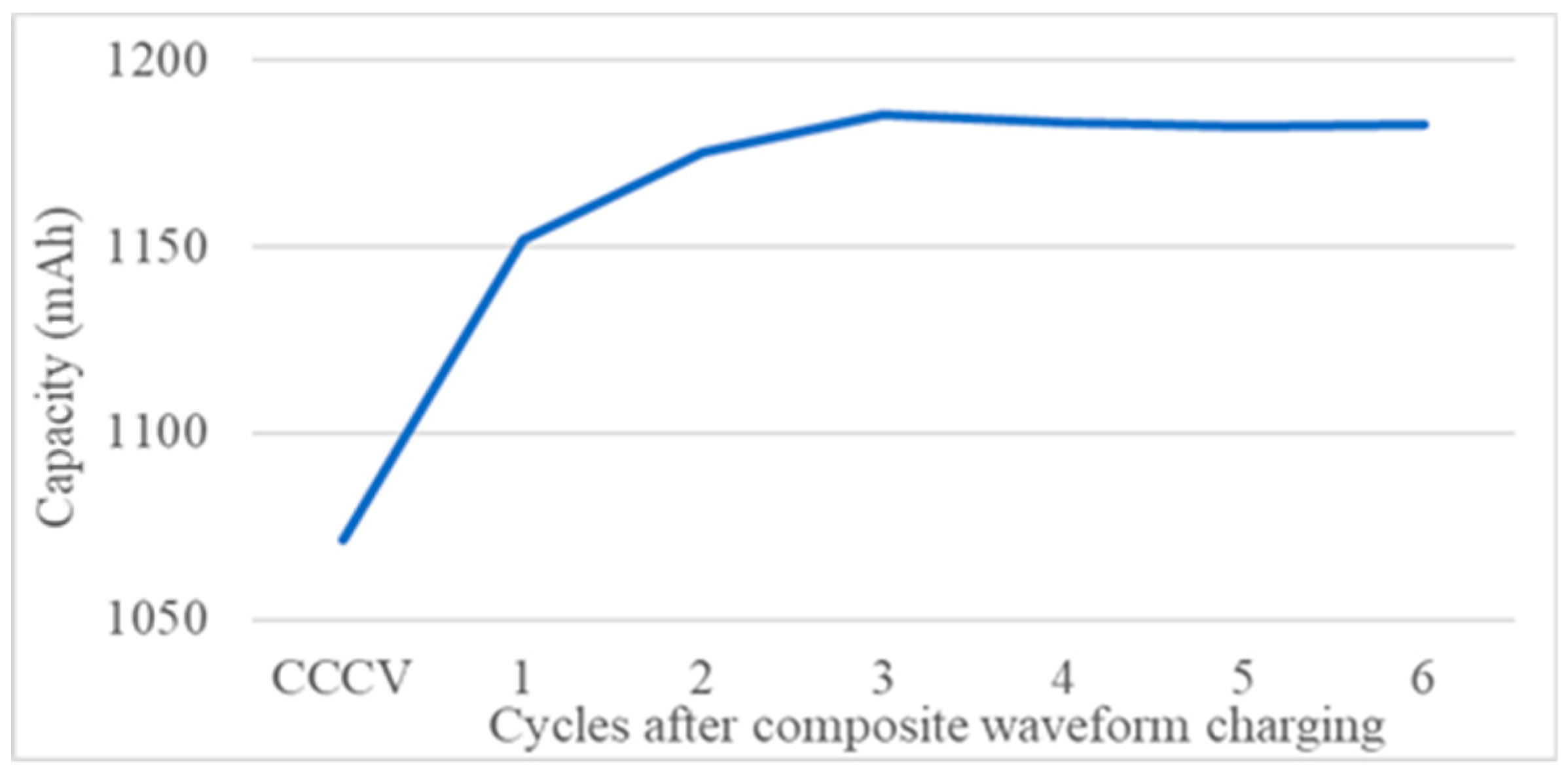
3.3. Verification of the Charging Circuit

The left portion of Figure 6a shows the microchip dsPIC30f4011 module. Through the RE0 pin, the PWM signal is sent to the gate driver, which is above the right side of the Printed Circuit Board (PCB) board. The gate driver drives the Complementary Metal-Oxide-Semiconductor (CMOS) architecture composed of PMOS and Negative Channel Metal Oxide Semiconductor (NMOS) on the left side of the PCB board. The output of power level PWM is restored to the composite charging waveform through the low-pass filter composed of wire-wound toroidal inductors, electrolytic capacitors, and ceramic capacitors on the right side of the PCB board. Adopting a 1.2 ohm cement resistor with a power of 20 W as the output load, a circuit load test is performed. The output voltage level will drop after the resistive load is connected. Therefore, a DC power supply is used for voltage compensation to increase the voltage from the original 5 to 6.2 V with the output current limited at 4.5 A. On passing through the charging circuit, the composite waveform output is generated. Figure 6b shows the final output of composite voltage and current waveforms, which display no discrepancy as compared with the desired target voltage waveform.
Effects of the circuit on the charging of the battery were then demonstrated. A LiFePO4 18650 battery (Pihsiang Energy Technology Co., Ltd.) was used. The original capacity of the battery was 1450 mAh. A conventional charging method with constant current–voltage of 5–3.7 V and constant current discharge of 5 A, with 600 charging–discharging cycles at room temperature, was used to age the battery. The charging and discharging processes have at least a 15 min rest between cycles, a 12 h rest every day, and a 60 h rest every weekend. The capacity of the aged battery was approximately 1065 mAh. Experiments of capacity recovery were then performed using the circuit to charge the aged battery. Figure 7 presents the results. After the first cycle involving charging using the composite waveform, the capacity increased to 1161 mAh, an improvement of approximately 6.7% from the original rated power was observed. In the following few cycles, the capacity was maintained at a high level. The maximum of recovery capacity is about 8%. The result is consistent with that of charge–discharge machine which we have done via commercial charging instrument [12].

4. Conclusions

The composite waveform generated by the circuit developed in this study can be comparable to the commercial charging instrument. The waveform voltage and current measured over the battery are identical in waveform. The major emphasis is on the generation of composite waveforms for future requirements that different batteries may adapt a variety of waveform parameters. The three practical contributions are as follows. First, parameters such as amplitude, frequency, voltage level, and waveform can all be incorporated into this study to generate a composite sinusoidal waveform on a large scale. Second, the circuit can be applied to charge the battery with a composite sinusoidal waveform in practical application. Both the voltage and current fall in the same ranges of those in the control group. Third, through the programed platform developed in this study, analog-to-digital signal can be predefined to be read as feedback, thereby allowing the future expansion with a database of waveform parameters. The cost of using such a digital method to generate charging waveform is quite low. The circuit was made with simple electronic components. It is expected to be widely used for charging single cell. However, whether it is suitable for the charging of battery packs remains to be studied. In addition, composite sinusoidal waveform charging is a novel method. Although some preliminary results have been reported, there are still many questions to be answered. We will keep report our demonstration data in future. However, if the self-made circuit developed by this study is adopted, researchers can also get rid of the limitations of commercial instruments and do more flexible research and development in future.

Author Contributions

Conceptualization, K.D.H. and P.-T.C.; methodology, F.-Y.Z. and X.-H.Z.; software, F.-Y.Z. and X.-H.Z.; validation, P.-T.C., R.-J.C. and K.D.H.; formal analysis, F.-Y.Z. and X.-H.Z.; investigation, F.-Y.Z. and X.-H.Z.; resources, C.-J.Y. and K.D.H.; data curation, X.-H.Z. and P.-T.C.; writing—original draft preparation, P.-T.C. and C.-J.Y.; writing—review and editing, P.-T.C. and C.-J.Y.; visualization, X.-H.Z.; supervision, R.-J.C., C.-J.C. and K.D.H. All authors have read and agreed to the published version of the manuscript.

Funding

In Authors thank the financial support from Ministry of Science and Technology, Taiwan, under grant number MOST 108-2113-M-002-021-MY2. The Center of Atomic Initiative for New Materials (AI-Mat) at National Taiwan University (108L9008), and the Featured Areas Research Center Program within the framework of the Higher Education Sprout Project by the Ministry of Education (MOE) in Taiwan are also acknowledged.

Conflicts of Interest

The authors declare no conflicts of interest.

References

  1. Barre, A.; Deguilhem, B.; Grolleau, S.; Gerard, M.; Suard, F.; Riu, D. A review on lithium-ion battery ageing mechanisms and estimations for automotive applications. J. Power Sources 2005, 241, 680–689. [Google Scholar] [CrossRef] [Green Version]
  2. Verma, P.; Maire, P.; Novák, P. A review of the features and analyses of the solid electrolyte interphase in Li-ion Batteries. Electrochim. Acta 2010, 55, 6332–6341. [Google Scholar] [CrossRef]
  3. Arora, P.; White, R.E.; Doyle, M. Capacity fade mechanisms and side reactions in lithium-ion batteries. J. Electrochem. Soc. 1998, 145, 3647–3667. [Google Scholar] [CrossRef] [Green Version]
  4. Thomas, E.V.; Bloom, I.; Christophersen, J.P.; Battaglia, V.S. Statistical methodology for predicting the life of lithium-ion cells via accelerated degradation testing. J. Power Sources 2008, 184, 312–317. [Google Scholar] [CrossRef]
  5. Amine, K.; Chen, C.H.; Liu, J.; Hammond, M.; Jansen, A.; Dees, D.; Bloom, I.; Vissers, D.; Henriksen, G. Factors responsible for impedance rise in high power lithium-ion batteries. J. Power Sources 2001, 97–98, 684–687. [Google Scholar] [CrossRef]
  6. Leng, F.; Tan, C.M.; Pecht, M. Effect of temperature on the aging rate of Li ion battery operating above room temperature. Sci. Rep. 2015, 5, 12967. [Google Scholar] [CrossRef] [PubMed] [Green Version]
  7. Li, J.; Murphy, E.; Winnick, J.; Kohl, P.A. The effects of pulse charging on cycling characteristics of commercial lithium-ion batteries. J. Power Sources 2001, 102, 302–309. [Google Scholar] [CrossRef]
  8. Thandiwe, I. Pulse Charging Circuit and Method; Motorola Inc.: Schaumburg, IL, USA, 2002. [Google Scholar]
  9. Benjamin, F. The reFLEX principle of charging nickel-cadmium and other batteries. In Proceedings of the IEEE Power Processing Electronics Specialists Conference, Atlantic City, NJ, USA, 22–23 May 1972; pp. 111–119. [Google Scholar]
  10. Chen, L.-R.; Wu, S.-L.; Shieh, D.-T.; Chen, T.-R. Sinusoidal-ripple-current charging strategy and optimal charging frequency study for Li-ion batteries. IEEE Trans. Ind. Electron. Control Instrum. 2013, 60, 88–97. [Google Scholar] [CrossRef]
  11. Chen, P.-T.; Yang, F.-H.; Sangeetha, T.; Gao, H.-M.; Huang, K.D. Moderate Energy for Charging Li-Ion Batteries Determined by First-Principles Calculations. Batter. Supercaps. 2018, 1, 209–214. [Google Scholar] [CrossRef]
  12. Chen, P.-T.; Yang, F.-H.; Cao, Z.-T.; Jhang, J.-M.; Gao, H.-M.; Yang, M.-H.; Huang, K.D. Reviving aged lithium-ion batteries and prolonging their cycle life by sinusoidal waveform charging strategy. Batter. Supercaps 2019, 2, 673–677. [Google Scholar] [CrossRef]
  13. Chen, P.-T.; Pai, P.-H.; Yang, C.-J.; Huang, K.D. Development of transmission systems for parallel hybrid electric vehicles. Appl. Sci. 2019, 9, 8. [Google Scholar] [CrossRef] [Green Version]
  14. Chen, P.-T.; Shen, D.-J.; Yang, C.-J.; Huang, K.D. Development of a hybrid electric motorcycle that accords energy efficiency and controllability via inverse differential gear and power mode switching control. Appl. Sci. 2019, 9, 1787. [Google Scholar] [CrossRef] [Green Version]
  15. Chen, P.-T.; Ding, P.-F.; Yang, C.-J.; Huang, K.D. Hybrid power system design for multifunctional mini loader vehicles. Appl. Sci. 2019, 9, 4439. [Google Scholar] [CrossRef] [Green Version]
  16. McCune, E. Time-filtered squarewave output from direct digital synthesis. In Proceedings of the 2010 IEEE MTT-S International Microwave Symposium, Anaheim, CA, USA, 23–28 May 2010; pp. 996–999. [Google Scholar]
  17. Ayesh, M.M.; Ibrahim, S.A.; Ragai, H.F.; Rizk, M.M. A low-power high-speed charge-steering ADC-based equalizer for serial links. In Proceedings of the 2015 IEEE International Conference on Electronics, Circuits, and Systems (ICECS), Cairo, Egypt, 6–9 December 2015; pp. 500–501. [Google Scholar]
  18. Payra, A.; Dutta, P.; Sarkar, A.; Sen, S.K. Design of a self regulated flash type ADC with high resolution. In Proceedings of the Michael Faraday IET International Summit 2015, Kolkata, India, 12–13 September 2015; pp. 591–595. [Google Scholar]
  19. High Performance Digital Signal Controllers. Available online: https://www.microchip.com/pressreleasepage/new-dsc-accelerates-dsp-performance-for-time-critical-control (accessed on 12 February 2020).
  20. Anushka, P.V.; Mani, N.; Issac, K. Switched-inductor semi-quadratic buck converter. In Proceedings of the 2017 International Conference on Technological Advancements in Power and Energy (TAP Energy), Kollam, India, 21–23 December 2017; pp. 1–6. [Google Scholar]
  21. Liu, S.; Liu, J.; Yang, Y.; Zhong, J. Design of intrinsically safe buck DC/DC converters. In Proceedings of the 2005 International Conference on Electrical Machines and Systems, Nanjing, China, 27–29 September 2005; pp. 1327–1331. [Google Scholar]
  22. Premalatha, L.; Vanajaranjan, P. Spectral analysis of DC-DC buck converter with chaotic dynamics. In Proceedings of the 2005 Annual IEEE India Conference-Indicon, Kollam, India, 11–13 December 2005; pp. 605–608. [Google Scholar]
  23. Li, Y.; Ji, Z. T-S modeling, Simulation and control of the buck converter. In Proceedings of the 2008 Fifth International Conference on Fuzzy Systems and Knowledge Discovery, Shandong, China, 18–20 October 2008; pp. 663–667. [Google Scholar]
  24. GKarim, H.; Golestanifar, A.; Ghaderi, A.; Salimpour, N. Ultra sharp transition-band low-pass filter with miniaturized size for GSM applications. Radio Eng. 2018, 27, 425–430. [Google Scholar]
  25. Cao, S.; Han, Y.; Chen, H.; Li, J. An ultra-wide stop-band LPF using asymmetric Pi-shaped koch fractal DGS. IEEE Access 2017, 5, 27126–27131. [Google Scholar] [CrossRef]
  26. Li, C.; Guo, B.; Li, N. Design on digital LPF for time domain harmonic detecting algorithm. In Proceedings of the 2009 IEEE 6th International Power Electronics and Motion Control Conference, Wuhan, China, 17–20 May 2009; pp. 2406–2410. [Google Scholar]
  27. Shi, J.; Yao, J.; Liu, K. Study on the method of GPS height interpolation in the linear measurement projects. In Proceedings of the 2011 International Conference on Electric Technology and Civil Engineering (ICETCE), Lushan, China, 22–24 April 2011; pp. 3553–3555. [Google Scholar]
  28. Tan, G.; Feng, Y.; Shen, H. A combined interpolation method for waveform reconstruction in beacon transmitter detector. In Proceedings of the IET International Communication Conference on Wireless Mobile and Computing (CCWMC 2011), Shanghai, China, 14–16 November 2011; pp. 270–273. [Google Scholar]
Figure 1. (a) Target waveform to be developed for the composite waveform charger; (b) Schematic of the investigated architecture.
Energies 13 00814 g001
Figure 2. (a) Direct digital synthesis; (b) Buck converter; (c) Working sequence diagram of the buck converter.
Energies 13 00814 g002
Figure 3. (a) Pulse width modulation (PWM) state; (b) Working sequence diagram; (c) π type filter; (d) Signal conversion between components.
Energies 13 00814 g003
Figure 4. (a) Developed verification waveform with 2.5 ± 0.5 V; (b) Amplitude increased to 2 V and level increased by 0.5 V; (c) Amplitude increased to 2 V and level decreased by 0.5 V; (d) Amplitude decreased to 0.5 V and level increased by 0.5 V; (e) Amplitude decreased to 0.5 V and level decreased by 0.5 V; (f) The composite waveform output with life-prolonging effects.
Energies 13 00814 g004
Figure 5. Overvoltage protection.
Energies 13 00814 g005
Figure 6. (a) Photo of the actual circuit; (b) Waveform of the output voltage.
Energies 13 00814 g006
Figure 7. Verification of the applied charging performance.
Energies 13 00814 g007

