Abstract
Rapid developments in energy storage and conversion technologies have led to the proliferation of low- and medium-power electric vehicles. Their regular operation typically requires an on-board battery charger that features small dimensions, high efficiency and power quality. This paper analyses an interleaved step-down single-ended primary-inductor converter (SEPIC) operating in the discontinuous conduction mode (DCM) for charging of battery-powered light electric vehicles such as an electric wheelchair. The required characteristics are achieved thanks to favourable arrangement of the inductors in the circuit: the input inductor is used for power factor correction (PFC) without additional elements, while the other inductor is used to provide galvanic isolation and required voltage conversion ratio. A modular interleaved structure of the converter helps to implement low-profile converter design with standard components, distribute the power losses and improve the performance. An optimal number of converter cells was estimated. The converter uses a simple control algorithm for constant current and constant voltage charging modes. To reduce the energy losses, synchronous rectification along with a common regenerative snubber circuit was implemented. The proposed charger concept was verified with a developed 230 VAC to 29.4 VDC experimental prototype that has proved its effectiveness.
1. Introduction
Developments in electronic systems together with improvements in battery technology enable spread of light electric vehicles (LEVs) in a wide range of applications: from electric bicycles, scooters and autonomous package carriers to utility vehicles and electric wheelchairs for disabled or elderly people [1,2,3,4,5]. Such applications typically employ a low-voltage battery (24–48 V nominal) and are charged from the AC grid with power up to 1 kW [6,7,8,9,10]. The chargers generally include two-stage ac-dc converters with a power factor pre-regulator (PFP) that is followed by a dc-dc converter [11,12,13] Such systems generally include a DC-bus formed by high voltage (>350 V) electrolytic capacitors [14,15], which are among the most critical parts of power electronic converters in terms of reliability [16].
Different solutions based on a variety of single-stage systems without DC-link have been proposed: resonant LLC topology [17,18], boost full bridge converter [19], flyback [20,21], SEPIC (single-ended primary-inductor converter) [22], quasi-resonant bridgeless converter [23], matrix converter [24], and dual active bridge [25]. Furthermore, a range of hybrid topologies have been introduced for PFC applications, such as: SEPIC-flyback [26], boost-flyback [27,28], boost-forward [29,30], and forward-flyback [31].
As compared to other single-stage converters, the SEPIC operating in discontinuous conduction mode (DCM) features important advantages: the voltage follower mode allows the current control loop to be omitted, while galvanic isolation provides for several isolated outputs. Moreover, the primary transistor turns on with zero voltage switching (ZVS), and the output diode turns off with zero current switching (ZCS).
Modern design approaches allow easy integration of batteries into various parts of the EV to achieve better ergonomics. For example, two separate batteries can be integrated into armrests of the wheelchair for easier access and swapping [1]. Optimal charging of such systems would require a charger with multiple outputs and charge balancing functionality. In addition, the charger should be compact and fit special on-board compartment for easy deployment upon necessity.
Present study focus is on the further development of the interleaved SEPIC concept recently proposed as a candidate topology for the battery charger of power-assist wheelchairs [32]. According to the specification, the charger is stored in a compartment under one of the armrests. The dimensions available are limited to 125 × 149 × 40 mm, as shown in Figure 1. To realise such low-profile design, the modular approach is implemented. It allows the distribution of the power between the interleaved cells, avoiding bulky components. As a result, the charger with low profile can be realised with standard components in accordance with the design specifications. Such configuration can also bring benefits in other applications due to the possibility of charging several devices simultaneously.
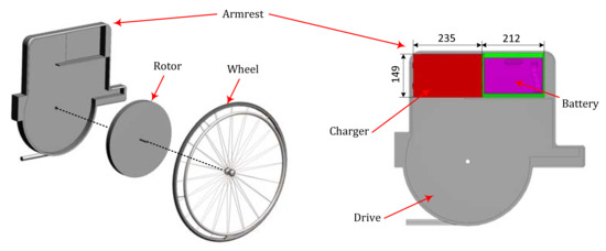
Figure 1.
Part of the power-assist wheelchair [2]; the compartment for the charger is located in the armrest (dimensions in mm).
Section 2 analyses the SEPIC and estimates the number of interleaved cells. Section 3 addresses the topology configuration and its control strategies for different charging modes. Section 4 is devoted to the description of the flyback regenerative snubber implemented to reduce voltage overshoots. The final converter prototype layout is presented in Section 5, followed by the experimental verification in Section 6. Finally, the conclusions are drawn in Section 7.
2. Analysis of the Modular SEPIC for PFC Application
The number of cells of a modular SEPIC has an impact on the input current quality parameters: power factor (PF) and total harmonic distortion (THD). Theoretical considerations addressed in this section will help to define the number of cells N for given values of quality parameters.
2.1. SEPIC Cell Model
The isolated version of the SEPIC topology in Figure 2a features a transformer instead of the second inductor to provide required voltage conversion ratio, along with galvanic isolation. Our assumptions in the analysis were as follows:
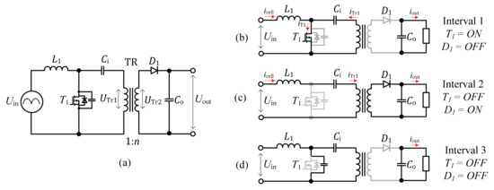
Figure 2.
Isolated single-ended primary-inductor converter (SEPIC) topology (a); equivalent circuits (b–d).
- All the elements of the SEPIC are lossless;
- Capacitors Ci and Co are large enough to neglect the voltage ripple across them;
- PWM switching period T is significantly shorter than the fundamental input voltage period Θ (T << Θ); therefore, the input voltage uin during the switching period has approximately constant value.
SEPICs operating in DCM can be represented by three equivalent circuits, as shown in Figure 2b–d. When the transistor S1 is turned on during the first interval (Figure 2b), the cell input current icell rises from zero value to maximum value Icell_max as follows:
where Uin is the input voltage value, L1 is the inductance value of the input inductor (Figure 2).
During the second interval, the cell input current declines to zero (Figure 2c):
where Ub is the output battery voltage, t0 is the duration of the third interval (DCM).
During the third interval (Figure 2d), the cell input current is zero, icell = 0. In the practical circuits, this mode is typically accompanied with oscillations that occur due to the presence of parasitic circuit components.
Two SEPIC cells connected in parallel and operating with a 180° phase shift can provide continuous input current iin, since in this case, it will be formed by the sum of currents in the two cells icell1 and icell2 (see Figure 3a). However, increased duration of DCM results in a more distorted input current [32]; therefore, it has to be minimised and the converter should preferably operate close to the boundary conduction mode (BCM).
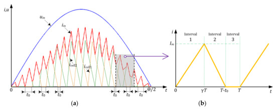
Figure 3.
Generalised input current of a two-cell converter: (a) current shape of an interleaved SEPIC; (b) representation of the cell input current waveform.
According to Equation (2), during the second interval, the current declines with a constant slope, which is determined by the output voltage Ub. Therefore, the third interval with zero input current has a varying interval of t0, which is inversely proportional to the input voltage Uin. Assuming the constant pulse width γ·T [32], the optimal operating mode can be achieved with BCM provided at the maximum input voltage Uin_max and DCM at lower Uin values, as depicted in Figure 3a.
For a sinusoidal grid voltage with a period Θ, uin = Uin_max sin(2 πt/Θ), the grid current generated with one SEPIC cell operating with a switching period T may be represented based on piecewise linear functions, which are characterised by interval durations and current slopes (see Figure 3b).
The current slope kr on the first interval when the current increases is
The peak current Im during the first interval is calculated according to Equation (1), where t = γ·T.
During the second interval, current decreases with the constant slope kf, which is determined by the peak current value Im. To obtain maximum PF, the value of kf is chosen for providing BCM (t0 = 0) at the points 2 πt/Θ = π/2 + πm, where m is an integer. However, in the practical converter, minimal zero current duration t0_min should be defined to avoid entering continuous conduction mode (CCM).
The current at the point φ = 2 πt/Θ = π/2 of the grid current is
where t′ is relative time since the beginning of the switching period, Im is the peak cell current during the first interval.
Hence, the current slope kf on the second interval is kf = Im/(T − t0_min − γT). For the other intervals, the input current slope results in a different t0 duration:
where the sign “−” corresponds to a positive sine wave and “+” to the negative one.
According to (4) and (5), the cell current can be estimated for an arbitrary value of the input current phase φ:
2.2. Estimation of the Number of SEPIC Cells Based on Current Quality Parameters
According to the analysis in the previous section, although sinusoidal input current can be achieved with two interleaved SEPIC cells, its quality can be compromised due to the presence of DCM intervals, particularly around zero crossings of the grid voltage. Increasing the number of interleaved cells can solve this issue, while keeping the constant pulse width γ·T. Another advantage lies in the reduction of current stresses of the individual cells, which enables distributed power dissipation and design using more compact components.
The total input current iΣ(t) for a predefined number of cells N is estimated as:
After defining the current of each cell with Equation (6) and substituting that in Equation (7), it is possible to calculate the RMS current value IΣRMS and the first harmonic value IΣ(1) to estimate PF and THD values:
where φ(1) is the phase shift between the first harmonics of the grid voltage and current.
As was mentioned, the maximum PF and minimum THD values are achieved when t0 = 0; therefore, the modular converter mostly operates close to this mode. Figure 4 shows PF and THD for the BCM mode with t0 = 0 with the given cell number N.
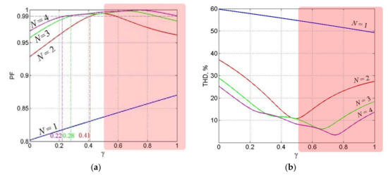
Figure 4.
Input current quality parameters vs. duty cycle γ and cell number N: (a) PF; (b) THD.
As was observed, PF and THD values improve with the increased duty cycle γ until a certain critical value γcr > 0.5, for instance, if N = 4, γcr ≈ 0.77. However, due to high voltage stress across the main transistor UT1_max, the duty cycle range should be limited within γ ϵ [0, 0.5]. The steady state voltage stress across the main MOSFET is calculated as follows:
The duty cycle range γ ϵ (0.5, 1] marked with the red area in Figure 1 is avoided. Among the allowed duty cycle γ range, the subrange with PF > 0.99 is selected from the SEPIC regulating characteristics:
The cell number N used for battery charging in the predefined voltage range Ub = 17.5–29.4 V can be determined according to Table 1.

Table 1.
Duty cycle range for battery charging in the predefined range Ub = 17.5–29.4 V.
As follows, the charger may consist of only three cells, N = 3. However, in order to improve redundancy, ensure the possible range of regulation and counter various manufacturing tolerances that may impact the conversion factor, the number of cells chosen for the current design is 4. With the cell number N = 4, the charger PF exceeds 0.99 for the wider range of γ. It is possible to estimate the resulting average PF during the whole charging process after analysing the charging control strategies.
3. Charger Configuration and Control Strategies
3.1. Charger Configuration
The charger developed for the considered wheelchair application should provide separate galvanically isolated output for charging each of the two installed batteries. In the configuration presented in Figure 5, the SEPIC cells have two secondary windings. The batteries are connected to one of the secondary windings of each SEPIC cell, which allows natural charge balancing when the initial state of the charge (SOC) of batteries is different. The arrangement provides for modular design with standard low-cost components and low-profile converter design. Potentially, such a configuration can be extended to provide charge to individual cells within a battery.
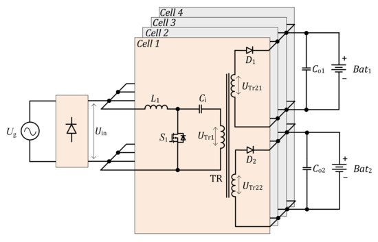
Figure 5.
Configuration of the proposed 4-cell modular interleaved charger based on SEPIC cells with two isolated outputs.
3.2. Constant Current and Constant Voltage Charging Modes
In the current work, the battery is charged with the standard constant current/constant voltage method (CC/CV). To ensure operation close to the BCM (t0_min → 0) for both CC and CV modes, a special modulation method for the SEPIC cells is required.
In the CC mode, the cell current has a constant average value Icell = ICC and voltage increases gradually from Ub_min = 17.5 V to Ub_max = 29.4 V. With the constant RMS value of the grid voltage (Uin=const), the CC mode is accompanied with gradually increasing (together with Ub) RMS value of the grid current Iin from the minimal value Iin_min to the maximal value Iin_max:
where ηcell is the SEPIC cell efficiency.
Increased input current results in an increased duration of the first and second intervals (Figure 3b) estimated according to Equations (1) and (2), respectively. At the same time, increased battery voltage leads to a decreased duration of the second interval. Therefore, different operating modes are required to implement the battery charging function.
Initially, for the (low) battery voltage Ub1, the converter cell operates in BCM with t0 = 0, its operation period is T1, the pulse duration is γ1·T1, and the input current is Iin1. After a certain time, the battery voltage is increased by the value ΔUb. Then the input current Iin2 is changed by the value ΔIin:
And the pulse duration γ2·T2 is estimated according to Equation (1):
The DCM duration (1 − γ2) T2, on the one hand, is increased together with the pulse duration γ2·T2; on the other hand, it is decreased with Ub. The equation for the estimation of DCM duration (1 − γ2) T2 is:
After substitution of the current Iin2 and the voltage Ub2, we obtain
which indicates the permanent duration of the DCM, i.e., (1 – γ2)·T2 = (1 – γ1)·T1. Therefore, for the CC mode, pulse frequency modulation (PFM) with constant off-time is provided, as depicted in Figure 6a.
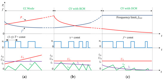
Figure 6.
Generalised representation of the implemented charging modes: (a) CC mode; (b) CV mode with BCM; (c) CV mode with DCM (input current iin, battery current ib and voltage Ub, control signal uc, output power P and switching frequency f).
In the CV mode, the battery voltage is constant, Ub = UCV, and the current ib is exponentially reduced:
where t′ is time from the beginning of the CV mode, and τ is the decay rate.
During the CV charging mode, the converter operates in BCM with PFM at the constant duty cycle, γ = const, as shown in Figure 6b. The PFM frequency is inversely proportional to the battery current ib. The typical practice is to finish the charging process when the current in the CV mode reduces to 0.05 C [33]. For the nominal charging rate of 0.5 C, it is required to change the switching frequency in the range of 1:10 to keep the SEPIC in the BCM. Since this range is difficult to implement in the practical converter, in the designed system, it is limited by a predefined value of fmax. If the frequency f reaches the maximum value fmax, the cell starts to operate in DCM with PWM and constant frequency fmax, as depicted in Figure 6c.
In the PWM mode, the battery current ib depends on the duty cycle γ as follows:
where kb is a constant coefficient.
As it follows from Equation (19), the current regulation in the range 10%–100% of ICC can be achieved with the duty cycle regulation of 1:3.1. Hence, during the whole charging process:
- -
- In the CC mode, the PFM modulation with battery current stabilisation and BCM detection is used;
- -
- In the CV mode with BCM, the PFM with battery voltage stabilisation is used;
- -
- In the CV mode with DCM, the PWM with battery voltage stabilisation is used.
3.3. Boundary Conduction Mode Control
The described control strategies require an effective and preferably simple method of the BCM detection. Figure 7 depicts generalised operating waveforms during one fundamental half-period of the rectified grid voltage uin. The DCM duration t0(k+2) should have its minimum value at the voltage maximum Uin_max. Therefore, the converter operating parameters should be chosen such that BCM is achieved at this point.
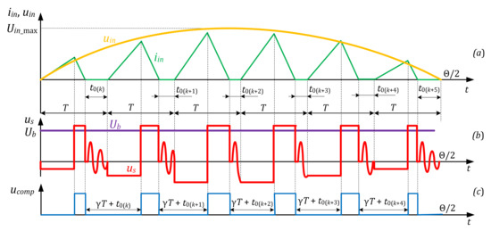
Figure 7.
Illustration of the BCM detection: (a) cell input current iin; (b) transformer secondary voltage us; (c) comparator voltage ucomp.
DCM may be easily detected using the transformer secondary voltage us (Figure 7). As compared with the battery voltage Ub, the rectangular voltage pulses can be obtained (see Figure 7c). The high-level comparator signal corresponds to the second interval when the output diode is conducting. The low-level corresponds to the sum of the first interval (when the input transistor is switched on) and the third interval (DCM). Since the duration of the first interval is known and equals to the constant value γ·T during the fundamental half period Θ/2 of rectified voltage, the DCM interval t0 can be defined by subtracting γ·T from the duration of the low-level comparator voltage.
To minimise the converter dimensions and cost, the control of the BCM mode can be realised based on the signal from a synchronous rectifier driver DA1 at the output of the SEPIC cell, as shown in Figure 8.
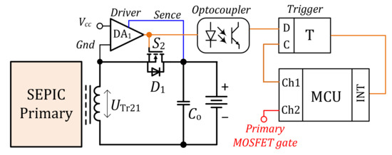
Figure 8.
Simplified circuit for BCM realisation using a synchronous rectifier driver.
The synchronous transistor control signal generated by the driver DA1 is used for DCM detection using “D” input of a trigger. Simultaneously, the trigger input “C” gets the signal from Ch 1 of the MCU PWM unit that is synchronised with Ch 2, which controls the input transistor S1 according to the principle shown in Figure 9. Due to the configurable pulse width of Ch 1 PWM signal uch1, a predefined DCM duration Δγ·T can be achieved. Otherwise, a low-level interrupt signal is generated and MCU increases the period of PWM from T to T + ΔT value.
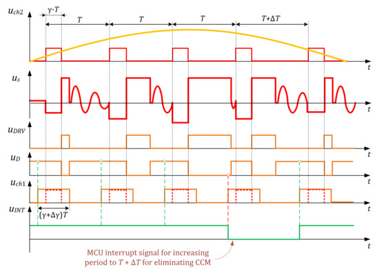
Figure 9.
Timing diagrams for BCM control (secondary winding voltage us, synchronous rectifier uDRV, trigger input uD, channel 1 of PWM uch1, and MCU interrupt input uINT).
The described method shifts all the high frequency control to external ICs and allows the use of the MCU resources only for the control of the battery charging process. Thus, within one fundamental period, the charger control is provided with PWM, while throughout the whole charging process (Figure 6), a more sophisticated control is used. A generalised realisation principle of CC and CV modes during the charging process is presented in Figure 10. As shown, the parameter recalculation is performed at the points with maximum rectified voltage by generating signal uINT. These parameters are then implemented at the beginning of the next grid half-period.
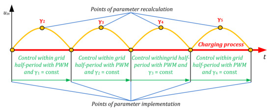
Figure 10.
Generalised representation of control within the fundamental period and throughout the whole charging process.
3.4. Calculation of Average Power Factor of the Battery Charger
During the battery charging, the duty cycle γ is increased from the minimal γmin to the maximum γmax value. At the same time, the PF is also changed accordingly. As shown before, the chosen duty cycle range γ ϵ [0.22, 0.5] allows regulation of the battery voltage in a much wider range (17.5–62.0 V) than necessary for the case study system (17.5–29.4 V). This enables estimation and choice of the duty cycle range γ ϵ [γmin, γmax], which provides the maximum average PF. A relation between γmin and γmax from the battery voltage range Ub_min = 17.5 V, Ub_max = 29.4 V can be defined as:
Expressing γmax from Equation (20), we obtain:
where ku = Ub_min/Ub_max.
According to Equation (20) for γmin = 0.22, γmax = 0.321, and for γmax = 0.5, γmin = 0.373. Therefore, γmin can vary in the range of [0.22, 0.373] and γmax in the range of [0.321, 0.5].
Average power factor, PFav can be calculated as follows:
where Tcharge is the charging time, and p(t) is the instantaneous power used as a weighting factor.
Equation (22) describing the charging modes may be rewritten as:
where TCC, TCV_BCM, TCV_DCM are charging time intervals in CC, CV with BCM and CV with DCM modes, respectively, ub, ib are instantaneous battery voltage and current.
In CC mode battery, voltage is linearly changed with time:
The battery current in the CV mode can be calculated by Equation (18). For Li-ion batteries, the typical CC mode duration can be more than one hour, whereas the total charging time is around three hours [34,35]. Therefore, the CC mode duration can be assumed as one third of the total charge time, TCC = Tcharge/3. The interrelation between durations of the CV mode with BCM and the total duration of the CV mode depends on the frequencies of the relation maximum fmax and the minimum fmin, kf = fmin/fmax and the relation between the nominal ICC and the minimal charging current Imin, ki = Imin/ICC. It can be estimated as follows:
After substitution of all relations in Equation (23), the average PF is calculated depending on the γmin, which varies in the range [0.22, 0.373] for kf = 1/4. The dependence PF = f(γ) is shown in Table 2. As observed, it is preferable to operate with γmin = 0.373 when the PF is at its maximum value of 0.996.
Table 2.
Average estimated PF for different γ ranges.
4. Flyback Regenerative Snubber
Since the SEPIC transformer operation and design is similar to a flyback transformer, it is typically necessary to apply a snubber to eliminate voltage spikes caused by the transformer leakage inductance [36]. The standard solution is to suppress the spikes by an RCD snubber that dissipates the leakage inductance energy in the snubber resistor. On the other hand, higher efficiency can be obtained if the leakage energy is redirected to the converter input or output by using passive regenerative snubbers [37,38] or active ZVS or ZCS snubbers [39,40]. However, for the given four-cell SEPIC configuration, such solutions can be redundant and sub-optimal. Therefore, the proposed approach for the regeneration of leakage inductance energy is to collect it from all the cells to a common capacitor and then transfer to the output using an auxiliary flyback converter. The auxiliary function of the stored energy is to supply the converter control system.
A simplified schematic of the proposed modular SEPIC configuration with the flyback regenerative system is shown in Figure 11. Each cell features a low-power high-voltage diode Dcl placed near the transformer that transfers the leakage energy released after turn-off of the main MOSFET to capacitors C2 and C3. These capacitors are used as an input source for the auxiliary flyback converter that transfers the energy to the load. Additional circuit with the diode Dc provides energy for the control system from the AC grid when the charger is not operating.
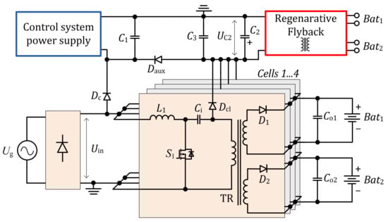
Figure 11.
Simplified schematic of 4-cell SEPIC with the flyback regenerative snubber and auxiliary supply.
The control system power supply consumes approximately constant power (around 1 W), while the regenerative flyback operates only if the capacitor C2 voltage UC2 is greater than the minimal value UC2_min, UC2 > UC2_min. Minimal voltage UC2_min must exceed the maximum output voltage reflected to the transformer primary winding UC2_min > Ub/n to avoid consumption of the SEPIC cell primary energy by the regenerative system. Since with chosen γ ϵ [0.37, 0.5], the reflected output voltage would not exceed maximum input voltage, the regenerative flyback has to operate only when:
If the condition (26) is not satisfied, the regenerative flyback stops its operation.
The capacitor C2 is calculated as a filter, taking into account the double grid frequency fg and the regenerative system power Pr:
where ΔUC2 is capacitor voltage ripple.
Capacitor C1 is charged together with the capacitor C2, and the voltage overshoots from leakage inductance appear on the voltage UC1_max:
The capacitor C1 energy is used to supply the control system. The value of C1 should be chosen such that it would not discharge to a voltage less than Uin_max:
where Pcs is the power consumed by the control system, and freg is the converter operating frequency.
Capacitor C3 is placed close to the SEPIC transformers to limit the voltage overshoots caused by the leakage inductance. Therefore, its capacitance is determined by the admissible voltage level at the converter transistor S1. Assuming that the maximum voltage overshoot is ΔUT1, the C3 value is:
where Lk is the leakage inductance, Ub_max is the maximum battery voltage, Ipr_max is the transformer primary winding peak current, n is the transformer ratio, Umax is the maximum output voltage.
The other elements of the regenerative system are selected according to general rules. The implemented regenerative system shown in Figure 12a is based on a typical low-power flyback topology with an intelligent device TinySwitch-4 [41].
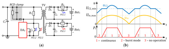
Figure 12.
Flyback regenerative converter: circuit (a); operation timing diagrams (b).
According to the design, the regenerative flyback has to operate only when the voltage level at the capacitor C2 exceeds the value UC2_min, which is defined with the resistor R2 = 13 MΩ to set UC2_min = 325 V [41].
The generalised operation principle of the regenerative flyback is illustrated in Figure 12b. As shown, the leakage inductance energy is mostly generated when the rectified input voltage is close to the maximum value. In this case, the capacitor C2 voltage is increased, which activates the regenerative flyback and it starts to operate continuously with maximum power (mode 1). When the input voltage reaches an intermediate value, the regenerative system operates in a burst mode (mode 2). During the low input voltage, all the energy is consumed by the control system and the regenerative flyback operation is stopped (mode 3).
For the experimentally measured value of the transformer leakage inductance Lk = 20 μH, the regenerative power Pr of the flyback is calculated as follows:
where N = 4 is the SEPIC cell number, fmin = 30 kHz is the minimum operation frequency of the SEPIC cell, Ipr_max = 2.7 A is the maximum cell current.
The regenerative flyback component values chosen for the total power Pr = 9 W at the maximum output voltage Umax = 30 V are shown in Table 3.
Table 3.
Main components of the regenerative flyback snubber.
5. Converter Design and Layout
The modular SEPIC charger was designed for fmin = 30 kHz, fmax = 120 kHz, and cell power Pcell = 100 W [32]. According to the design specifications, the dimensions of the battery charger printed circuit board (PCB) are limited to 230 × 145 mm. The maximum height of the elements is varied from 25 to 35 mm. The final placement of the elements in the given volume is depicted in Figure 13. The largest components (input inductors L1, transformers TR, output capacitors CO, regenerative flyback transformer TV) are placed in the middle or around the edges of the PCB. As a result, the 4-cell structure of the charger was implemented without exceeding the required application limits. The types and dimensions of the important components are listed in Table 4.
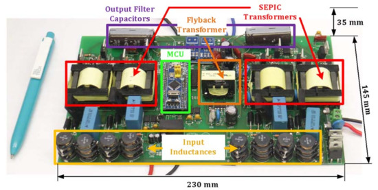
Figure 13.
Photo of the modular charger prototype.
Table 4.
SEPIC cell component parameters.
6. Experimental Results
This section is devoted to the experimental verification of the developed modular SEPIC-based charger and its components. The following functions and operating characteristics are addressed in detail:
- BCM of input current provided by logic circuits and MCU interrupt generation;
- Operation of regenerative flyback snubber;
- Verification of voltage and current stresses on main components: primary MOSFETs, transformers and rectifier transistors;
- Validation of PF, THD and efficiency during battery charging in CC and CV modes.
6.1. Verification of Operation in BCM
For the case study charger, the BCM and DCM are the main operating modes, therefore, t0 duration should be stable and easily configurable. As described in the previous section, the synchronous rectifier gating signal, except its direct function of reducing losses, is also used to control the DCM duration. As Figure 14 shows, the synchronous rectifier on-time increases together with the input voltage. The DCM detection is clearly demonstrated in Figure 15a,b, when the feedback is open and the microcontroller does not respond to the interrupt signal.
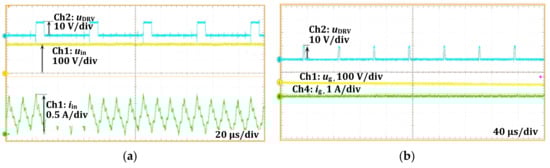
Figure 14.
Timing diagrams of a synchronous rectifier: (a) near maximum value of grid voltage; (b) near zero value of grid voltage
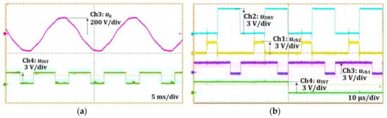
Figure 15.
Timing diagrams of zero current pause detection: (a) interrupt signal within several periods of grid voltage; (b) interrupt signal falling edge.
In the proposed control method, the interrupt signal uINT appears when the duration of the zero-current interval t0 is less than that predefined with the duty cycle value of uch1, see Figure 9 and Figure 15b. Since the DCM duration decreases as the input voltage uin rises, the interrupt signal uINT is symmetrically positioned relative to the amplitude value of the voltage, as shown in Figure 15a. The falling edge of the interrupt signal uINT appears when the synchronous rectifier signal uDRV is high at the rising edge of the PWM signal uch1 (see Figure 15b). When the interrupt is activated, the DCM duration is regulated only during one period of PWM, which prevents the converter from entering the CCM.
6.2. Verification of Regenerative Flyback Snubber
The operating waveforms of the implemented flyback snubber are presented in Figure 16. Since the filter capacitor C2 was chosen taking into account the grid frequency, it allowed to minimise the input voltage and output current ripple of the flyback, as shown in Figure 16a. The current value is defined by the optocoupler forward voltage that is approximately UF = 1 V.
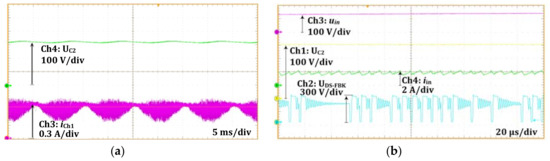
Figure 16.
Capacitor C2 voltage and flyback output current for several fundamental periods (a); switching waveforms of flyback when operating close to the continuous mode (b).
6.3. General Switching Waveforms
The experimental waveforms presenting the formation of continuous grid current are presented in Figure 17a. As shown, despite DCM, the resulting input current ripple is significantly reduced thanks to interleaving of the four SEPIC cells. The effect of flyback snubber depicted in Figure 17b shows that the peak voltage overshoot across the main MOSFET was limited to approximately 600 V. The operational waveforms of the synchronous rectifier MOSFET and SEPIC transformer are demonstrated in Figure 18.
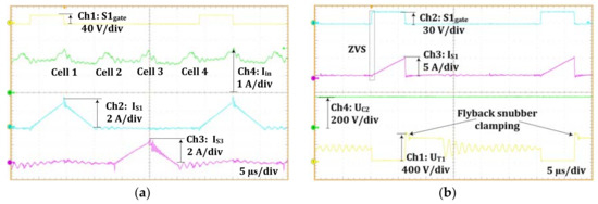
Figure 17.
Experimental waveforms for CV-DCM: formation of continuous input current (a), limitation of S1 transistor overvoltage by the regenerative flyback snubber (b).
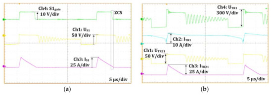
Figure 18.
Experimental waveforms CV-DCM: operation of the synchronous rectifier MOSFETs (a), SEPIC transformer currents and voltages (b).
The voltage and charging current waveforms of equally charged batteries are depicted in Figure 19a, while the case with batteries at uneven charge is presented in Figure 19b. As shown, the battery with lower voltage (and SOC) is being supplied with larger current. In both cases, the double grid frequency ripple (100 Hz) can be clearly observed, which is the peculiarity of the SEPIC topology. This ripple can be reduced by applying larger output filter capacitors. Nevertheless, according to assumptions in previous studies, its negative impact on Li-ion batteries is incognisant [42].
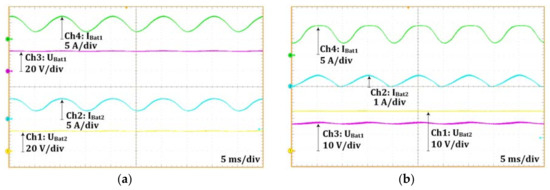
Figure 19.
Voltage and currents of batteries during charging: equally charged batteries (a); unbalanced batteries (b).
6.4. Verification of PF, THD and Efficiency During the Charging Process
The batteries used in the current case study are based on LG 18650 MJ1 3500 mAh cells (7 series, 4 parallel). To estimate average weighted efficiency, THD and PF, it is necessary to analyse converter operation during different charging modes. Examples of the input current shapes during different operating modes are presented in Figure 20. The operating parameters estimated taking into account the charge profile of the case study batteries are shown in Figure 21.
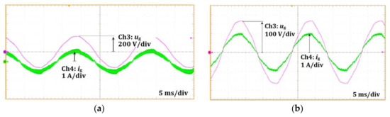
Figure 20.
Grid voltage and current waveforms: for γ = 0.25 (a); for γ = 0.5 (b).
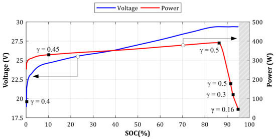
Figure 21.
Charge profile of the case study batteries corresponding to the standard charging at 0.5 C.
According to the experiments, for γ ϵ [0.15; 0.5] that was used for charging, the grid current shape is very close to sinusoidal. The experimentally obtained THD and PF of the grid current for different γ are listed in Table 5 and the efficiency is shown in Figure 22.
Table 5.
Experimentally measured values of THD and PF.
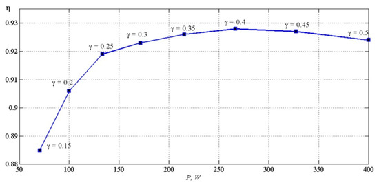
Figure 22.
Experimental charger efficiency vs. power.
7. Discussion and Conclusions
The paper has introduced a novel concept of a modular PFC charger based on the interleaved SEPIC topology. The converter has two isolated outputs for simultaneous charging of two batteries integrated into armrests of a power-assist wheelchair. Thanks to the interleaved structure, the prototype features a low-profile power stage design of only 35 mm in height that was realised with standard components. Moreover, the charger features galvanic isolation from input to output, as well as between the two outputs.
Design and operation aspects of the proposed charger and its subsystems are presented and verified experimentally. The features required for the application were realised with a simple control strategy that also achieved high input current quality with PF > 0.99 and THD < 3%. Thanks to the natural state of charge balancing and low height, the concept can be suitable for other applications that require simultaneous charging of different batteries or integration in a low-profile frame.
Author Contributions
Conceptualization, I.V. and A.B.; investigation, A.B. and I.G.; methodology, I.V.; software, D.Z.; supervision, D.V.; validation, A.B. and D.Z.; writing—original draft, I.V. and A.B., writing—review and editing, D.V.; project administration, D.V. and I.G.; funding acquisition, D.V. and A.B. All authors have read and agreed to the published version of the manuscript.
Funding
The preparing of this publication is supported by the European Regional Development Fund (ERDF) within the contract Nr. 1.1.1.1/16/A/147 “Research and Development of Electrical, Information and Material Technologies for Low Speed Rehabilitation Vehicles for Disabled People”, by the Estonian Centre of Excellence in Zero Energy and Resource Efficient Smart Buildings and Districts, ZEBE, grant 2014-2020.4.01.15-0016 funded by the European Regional Development Fund and by EEA Financial Mechanism 2014-2021 under Grant EMP474.
Conflicts of Interest
Authors declare no conflict of interest.
Nomenclature
| f | SEPIC cell switching frequency |
| fg | grid fundamental frequency |
| fmax, fmin | maximum and minimum SEPIC cell switching frequency |
| freg | flyback snubber switching frequency |
| ICC | charging current in constant current mode |
| icell | cell input current |
| Im | peak current value of the cell |
| Iin_min, Iin_max | minimum and maximum grid current RMS values during charging |
| Ipr_max | peak current of the flyback transformer primary winding |
| iΣ | total input current |
| kr | constant slope of the cell input current rising edge |
| kf | constant slope of the cell input current falling edge |
| L1 | inductance value of the SEPIC input inductor |
| n | transformer turns ratio |
| N | number of charger cells |
| Pr | regenerative system power |
| Pcs | control system consuming power |
| T | switching period |
| TCC | charging time intervals in CC mode |
| TCC_BCM | charging time intervals in CC with BCM mode |
| TCC_DCM | charging time intervals in CC with DCM mode |
| Tcharge | battery total charging time |
| t | time variable |
| t′ | time since the beginning of the switching period |
| t0 | duration of zero current interval |
| t0_min | minimal duration of zero current interval |
| ub, ib | instantaneous battery voltage and current |
| Ub_min, Ub_max | battery minimum and maximum charging voltages |
| UC1_max | maximum voltage of the control system power supply capacitor C1 |
| UC2 | voltage of the flyback input capacitor C2 |
| UF | optocoupler forward voltage |
| ug | instantaneous grid voltage |
| uin, iin | instantaneous rectified voltage and current |
| Uin_max | maximum rectified voltage |
| us | secondary voltage of SEPIC transformer |
| ΔUC2 | C2 capacitor voltage ripple |
| ΔUT1 | maximum voltage overshoot of input SEPIC transistors |
| Θ | fundamental period of the grid |
| φ | input current phase |
References
- Keller, S.; Christmann, K.; Gonzalez, M.S.; Heuer, A. A Modular Fuel Cell Battery Hybrid Propulsion System for Powering Small Utility Vehicles. In Proceedings of the IEEE Vehicle Power and Propulsion Conference (VPPC), Belfort, France, 11–14 December 2017; pp. 1–4. [Google Scholar]
- Galkin, I.; Podgornovs, A.; Blinov, A.; Vitols, K.; Vorobyov, M.; Kosenko, R. Considerations regarding the concept of cost-effective power-assist wheelchair subsystems. Electr. Control Commun. Eng. 2018, 14, 71–80. [Google Scholar] [CrossRef]
- Bertoluzzo, M.; Buja, G. Development of Electric Propulsion Systems for Light Electric Vehicles. IEEE Trans. Industrial. Inform. 2011, 7, 428–435. [Google Scholar] [CrossRef]
- Hayashi, T.; Takahashi, Y. Small compact standing ride-type electric vehicle for shopping. In Proceedings of the 16th International Conference on Control, Automation and Systems (ICCAS), Gyeongju, Korea, 16–19 October 2016; pp. 238–243. [Google Scholar]
- Hayashi, T.; Takahashi, Y. Small compact electric vehicle for practical use and its repeated start-stop tests. In Proceedings of the 15th International Conference on Control, Automation and Systems (ICCAS), Busan, Korea, 13–16 October 2015; pp. 113–118. [Google Scholar]
- Kushwaha, R.; Singh, B. Power Factor Improvement in Modified Bridgeless Landsman Converter Fed EV Battery Charger. IEEE Trans. Veh. Technol. 2019, 68, 3325–3336. [Google Scholar] [CrossRef]
- Zhou, W.; Wattenberg, M.; Schwalbe, U. Design Considerations of a Single Stage LLC Battery Charger. In Proceedings of the International Exhibition and Conference for Power Electronics, Intelligent Motion, Renewable Energy and Energy Management, Nuremberg, Germany, 7–9 May 2019; pp. 1–7. [Google Scholar]
- Tsai, C.-C.; Lin, W.-M.; Lin, C.-H.; Wu, M.-S. Designing a fast battery charger for electric bikes. In Proceedings of the International Conference on System Science and Engineering, Taipei, Taiwan, 1–3 July 2010; pp. 385–389. [Google Scholar]
- Nguyen, C.; Primiani, P.; Viglione, L.; Woodward, L. A Low-Cost Battery Charger Usable with Sinusoidal Ripple-Current and Pulse Charging Algorithms for E-Bike Applications. In Proceedings of the IEEE 28th International Symposium on Industrial Electronics (ISIE), Vancouver, BC, Canada, 12–14 June 2019; pp. 2085–2090. [Google Scholar]
- Jalakas, T.; Zakis, J. Experimental verification of light electric vehicle charger multiport topology. In Proceedings of the 9th International Conference on Compatibility and Power Electronics (CPE), Costa da Caparica, Portugal, 24–26 June 2015; pp. 415–418. [Google Scholar]
- Yilmaz, M.; Krein, P.T. Review of Battery Charger Topologies, Charging Power Levels, and Infrastructure for Plug-In Electric and Hybrid Vehicles. IEEE Trans. Power Electron. 2018, 28, 2151–2169. [Google Scholar] [CrossRef]
- Blinov, A.; Kosenko, R.; Chub, A.; Vinnikov, D. Bidirectional soft-switching dc–dc converter for battery energy storage systems. IET Power Electron. 2018, 11, 2000–2009. [Google Scholar] [CrossRef]
- Blinov, A.; Kosenko, R.; Vinnikov, D.; Parsa, L. Bidirectional Isolated Current Source DAB Converter with Extended ZVS/ZCS Range and Reduced Energy Circulation for Storage Applications. IEEE Trans. Ind. Electron. 2019. [Google Scholar] [CrossRef]
- Martínez, F.G.; Magaldi, G.L.; Serra, F.M. Solar Charging Station for Small Electric Vehicles. In Proceedings of the Argentine Conference on Automatic Control (AADECA), Buenos Aires, Argentina, 7–9 November 2018; pp. 1–6. [Google Scholar]
- Wijesekera, A.; Binduhewa, P. Design of a Small Electric Vehicle Charger with Multi-Ports. In Proceedings of the 2nd International Conference on Electrical Engineering (EECon), Colombo, Sri Lanka, 28 September 2018; pp. 8–13. [Google Scholar]
- Falck, J.; Felgemacher, C.; Rojko, A.; Liserre, M.; Zacharias, P. Reliability of Power Electronic Systems: An Industry Perspective. IEEE Ind. Electron. Mag. 2018, 12, 24–35. [Google Scholar] [CrossRef]
- Saasaa, R.; Eberle, W.; Agamy, M. A single-stage interleaved LLC PFC converter. In Proceedings of the IEEE Energy Conversion Congress and Exposition (ECCE), Milwaukee, WI, USA, 18–22 September 2016; pp. 1–6. [Google Scholar]
- Lin, W.; Chen, H.; Fang, Y. A Single-stage PFC by Integrating quasi-Bridgeless Boost and LLC Converter. In Proceedings of the IEEE International Telecommunications Energy Conference (INTELEC), Turin, Italy, 7–11 October 2018; pp. 1–5. [Google Scholar]
- Zhang, Q.; Meng, T.; Ben, H.; Wang, W. Implementation of a start-up scheme for single-stage full-bridge boost PFC converter. In Proceedings of the IEEE Transportation Electrification Conference and Expo, Asia-Pacific (ITEC Asia-Pacific), Harbin, China, 7–10 August 2017; pp. 1–5. [Google Scholar]
- Chiu, H.; Lo, Y.K.; Lee, H.C.; Cheng, S.J.; Yan, Y.C.; Lin, C.Y.; Wang, T.H.; Mou, S.C. A Single-Stage Soft-Switching Flyback Converter for Power-Factor-Correction Applications. IEEE Trans. Ind. Electron. 2010, 57, 2187–2190. [Google Scholar] [CrossRef]
- Lee, J.; Kwon, J.; Kim, E.; Choi, W.; Kwon, B. Single-Stage Single-Switch PFC Flyback Converter Using a Synchronous Rectifier. IEEE Trans. Ind. Electron. 2008, 55, 1352–1365. [Google Scholar]
- Ewerling, M.V.M.; Font, C.H.I. Single-stage AC/DC converter based on sepic topology operating in continuous conduction mode. In Proceedings of the Brazilian Power Electronics Conference (COBEP), Juiz de Fora, Brazil, 19–22 November 2017; pp. 1–6. [Google Scholar]
- Scherbaum, M.; Reddig, M.; Kennel, R.; Schlenk, M. An Isolated, bridgeless, quasi-resonant ZVS-switching, buck-boost single-stage AC-DC converter with power factor correction (PFC). In Proceedings of the IEEE Applied Power Electronics Conference and Exposition (APEC), Tampa, FL, USA, 26–30 March 2017; pp. 74–81. [Google Scholar]
- Li, C.; Xu, D. Family of Enhanced ZCS Single-Stage Single-Phase Isolated AC–DC Converter for High-Power High-Voltage DC Supply. IEEE Trans. Ind. Electron. 2017, 64, 3629–3639. [Google Scholar] [CrossRef]
- Jauch, F.; Biela, J. Single-phase single-stage bidirectional isolated ZVS AC-DC converter with PFC. In Proceedings of the 15th International Power Electronics and Motion Control Conference (EPE/PEMC), Novi Sad, Serbia, 4–6 September 2012; pp. 1–8. [Google Scholar]
- Poorali, B.; Adib, E. Analysis of the Integrated SEPIC-Flyback Converter as a Single-Stage Single-Switch Power-Factor-Correction LED Driver. IEEE Trans. Ind. Electron. 2016, 63, 3562–3570. [Google Scholar] [CrossRef]
- Abasian, A.; Farzanehfard, H.; Hashemi, S.A. A Single-Stage Single-Switch Soft-Switching (S6) Boost-Flyback PFC Converter. IEEE Trans. Power Electron. 2019, 34, 9806–9813. [Google Scholar] [CrossRef]
- Lu, D.D. High Voltage Stress in Single-Phase Single-Stage PFC Converters: Analysis and an Alternative Solution. IEEE Trans. Ind. Electron. 2016, 63, 133–143. [Google Scholar] [CrossRef]
- Chow, M.H.L.; Lee, Y.S.; Tse, C.K. Single-stage single-switch isolated PFC regulator with unity power factor, fast transient response and low voltage stress. In Proceedings of the 29th Annual IEEE Power Electronics Specialists Conference (Cat. No.98CH36196), Fukuoka, Japan, 22–22 May 1998; Volume 2, pp. 1422–1428. [Google Scholar]
- Lu, D.D.; Iu, H.H.; Pjevalica, V. Single-Stage AC/DC Boost—Forward Converter with High Power Factor and Regulated Bus and Output Voltages. IEEE Trans. Ind. Electron. 2009, 56, 2128–2132. [Google Scholar] [CrossRef]
- Bodur, H.; Kaya, K.Y.; Akboy, E.; Aksoy, I. A new forward-flyback based single switch single stage PFC converter. In Proceedings of the IEEE 6th International Symposium on Power Electronics for Distributed Generation Systems (PEDG), Aachen, Germany, 22–25 June 2015; pp. 1–3. [Google Scholar]
- Galkin, I.; Blinov, A.; Verbytskyi, I.; Zinchenko, D. Modular Self-Balancing Battery Charger Concept for Cost-Effective Power-Assist Wheelchairs. Energies 2019, 12, 1526. [Google Scholar] [CrossRef]
- Verbytskyi, I.; Bondarenko, O.; Kaloshyn, O. Multicell-type charger for supercapacitors with power factor correction. In Proceedings of the Young Engineers Forum (YEF-ECE), Costa da Caparica, Portugal, 4 May 2018; pp. 91–96. [Google Scholar]
- Zhang, S.S. The effect of the charging protocol on the cycle life of a Li-ion battery. J. Power Sources 2006, 161, 1385–1391. [Google Scholar] [CrossRef]
- Patnaik, L.; Praneeth, A.V.J.S.; Williamson, S.S. A Closed-loop Constant-temperature Constant-voltage Charging Technique to Reduce Charge Time of Lithium-ion Batteries. IEEE Trans. Ind. Electron. 2019, 66, 1059–1067. [Google Scholar] [CrossRef]
- Yao, J.; Abramovitz, A.; Smedley, K. Analysis and design of charge pump-assisted high step-up tapped inductor SEPIC converter with an “inductor-less” regenerative snubber. IEEE Trans. Power Electron. 2015, 30, 5565–5580. [Google Scholar] [CrossRef]
- Meng, T.; Ben, H.; Zhu, L.; Wei, G. Improved passive snubbers suitable for single-phase isolated full-bridge boost power factor correction converter. IET Power Electron. 2014, 7, 279–288. [Google Scholar] [CrossRef]
- Tibola, G.; Lemmen, E.; Duarte, J.L.; Barbi, I. Passive Regenerative and Dissipative Snubber Cells for Isolated SEPIC Converters: Analysis, Design, and Comparison. IEEE Trans. Power Electron. 2017, 32, 9210–9222. [Google Scholar] [CrossRef]
- Yao, J.; Abramovitz, A.; Ma Smedley, K. Steep-Gain Bidirectional Converter with a Regenerative Snubber. IEEE Trans. Power Electron. 2015, 30, 6845–6856. [Google Scholar] [CrossRef]
- Yang, J.W.; Do, H.L. Soft-Switching Dual-Flyback DC–DC Converter with Improved Efficiency and Reduced Output Ripple Current. IEEE Trans. Ind. Electron. 2017, 64, 3587–3594. [Google Scholar] [CrossRef]
- TinySwitch-4. Available online: https://ac-dc.power.com/products/tinyswitch-family/tinyswitch-4/ (accessed on 2 October 2019).
- Bala, S.; Tengnér, T.; Rosenfeld, P.; Delince, F. The effect of low frequency current ripple on the performance of a Lithium Iron Phosphate (LFP) battery energy storage system. In Proceedings of the IEEE Energy Conversion Congress and Exposition (ECCE), Raleigh, NC, USA, 15–20 September 2012; pp. 3485–3492. [Google Scholar]


© 2020 by the authors. Licensee MDPI, Basel, Switzerland. This article is an open access article distributed under the terms and conditions of the Creative Commons Attribution (CC BY) license (http://creativecommons.org/licenses/by/4.0/).