Abstract
Various industrial applications require a voltage conversion stage from DC to AC. Among them, commercial renewable energy systems (RES) need a voltage buck and/or boost stage for islanded/grid connected operation. Despite the excellent performance offered by conventional two-stage converter systems (dc–dc followed by dc–ac stages), the need for a single-stage conversion stage is attracting more interest for cost and size reduction reasons. Although voltage source inverters (VSIs) are voltage buck-only converters, single stage current source inverters (CSIs) can offer voltage boost features, although at the penalty of using a large DC-link inductor. Boost inverters are a good candidate with the demerit of complicated control strategies. The impedance source (Z-source) inverter is a high-performance competitor as it offers voltage buck/boost in addition to a reduced passive component size. Several pulse width modulation (PWM) techniques have been presented in the literature for three-phase Z-source inverters. Various common drawbacks are annotated, especially the non-linear behavior at low modulation indices and the famous trade-off between the operating range and the converter switches’ voltage stress. In this paper, a modified discontinuous PWM technique is proposed for a three-phase z-source inverter offering: (i) smooth voltage gain variation, (ii) a wide operating range, (iii) reduced voltage stress, and (iv) improved total harmonic distortion (THD). Simulation, in addition to experimental results at various operating conditions, validated the proposed PWM technique’s superior performance compared to the conventional PWM techniques.
1. Introduction
The world’s increasing energy consumption, depleting fossil fuels, and environmental problems encourage the development of power electronic-based converters. The voltage source inverter (VSI) and the current source inverter (CSI) are commonly the main power inverters utilized in various industrial applications. However, both have the drawback of a limited voltage range operation. VSIs offer an inherited output voltage buck feature, whereas CSIs can present voltage boost capability. In order to obtain an additive ability such as boosting the VSI output or bucking the CSI output voltage, a separate stage of the DC–DC converter must be implemented [1,2,3,4,5,6,7,8]. Inserting a DC–DC converter stage before the inversion stage adds more control complexity in addition to increasing system cost and size. Consequently, boost inverters were introduced [9,10]. They have the capacity for voltage buck-boost in addition to DC to AC inversion using single-stage topology. However, they suffer complex control strategies.
Impedance source inverters (ZSIs) provide an enhanced power conversion capability with a similar functionality as boost inverters without inserting any extra active elements and with simple control strategies [11]. The concept of impedance source converters has been implemented for (i) AC–AC converters [12,13,14,15,16], (ii) DC–DC converters [17,18,19,20], (iii) AC–DC rectifiers [21,22,23,24] and (iv) DC–AC inverters [25,26,27,28,29,30,31,32,33,34]. Based on these merits, ZSIs start to penetrate various industrial application markets, such as electric vehicles [35,36,37,38,39,40], renewable energy-distributed generation [41,42,43,44,45,46], battery energy storage [47,48], and uninterruptable power supply (UPS) [49,50]. The basic ZSI topology introduced by Peng et al. [11] has an impedance network of linear energy storage elements (two capacitors and two- nductors) forming the X-shape network, as shown in Figure 1. Figure 1 represents a basic conventional z-source inverter. The topology is simply a three-phase inverter with an X-shaped passive circuit at its front. The added passive network alongside the adequate modulation technique adds voltage buck/boost capabilities to the inverter stage by means of shoot-through periods.
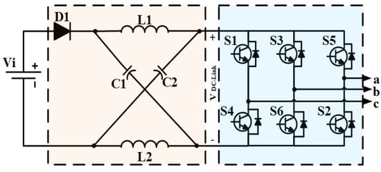
Figure 1.
Basic x-shaped topology for ZSI.
Adding nonlinear elements (diodes and switches) to the impedance network improves the performance of the converter by extending its voltage boost ability [27,28,29,30,31,32,33,34] or enhancing the DC-bus voltage and current profiles [25,26], with the penalty of increasing system cost, size and control complexity. Navigating through ZSIs’ PWM control techniques, several techniques have been introduced to coincide with various application requirements.
The Simple Boost ZSI PWM technique was the first z-source inverter PWM technique [11]. The technique is based on a VSI conventional sinusoidal PWM with two added fixed envelopes with magnitudes equal to or greater than the modulation index. The magnitude of those envelopes is limited to the modulation index value. Despite its simple implementation, the Simple Boost PWM technique has the major drawback of high voltage stresses across the inverter bridge power electronic switches [11].
Maximum Boost PWM (MBPWM) utilizes the instantaneous maximum/minimum of the three phase references as the upper and lower envelopes. A large reduction in voltage stresses is noticed, thanks to the enhanced boosting factor [51]. On the contrary, the unfixed envelopes’ difference exerts higher-magnitude low-frequency voltage ripples in the DC-link voltage six times the fundamental frequency. As a result, the Maximum Boost ZSI PWM technique features reduced voltage stresses with the penalty of increased cost and size of the impedance network [51].
The Constant Boost ZSI PWM technique was introduced to achieve a compromised voltage stress and impedance network cost and size [52]. The constant-difference variable-envelopes aid the Constant Boost PWM technique to achieve low DC-link voltage ripples with reasonable voltage stresses.
The Modified Space Vector ZSI PWM technique extends the operating range of the inverter with reduced voltage stresses, especially at high-voltage gain [53,54]. The utilized shoot-through state with evenly distributed active states succeeded in THD and switching losses’ reduction.
The previously mentioned PWM techniques attempt to improve ZSI performance by reducing the inverter bridge power electronic switches voltage stresses in addition to the size of the impedance network. Those techniques share common limitations such as:
- Only offering one degree of freedom from the control strategy point of view.
- A highly nonlinear performance at high-gain operating conditions.
- High sensitivity at low-modulation index operation.
- A common trade-off between extended operating conditions and voltage stresses.
In 2016, a PWM Technique for the high-voltage gain operation of three-phase Z-source inverters based on the discontinuous PWM technique for three-phased ZSI was introduced [55,56]. This enhanced performance technique overcomes several conventional ZSI PWM techniques’ problems. The core of the discontinuous PWM technique relies on separating the relation between the modulation index and the boosting factor, with a limited fixed modulation index at 1/√3 to avoid over-modulation [57].
Several review articles of z-source PWM techniques can be found in the literature for interested readers [58,59,60].
In this paper, an enhanced performance ZSI PWM technique is proposed based on the recently evolved discontinuous PWM for three-phase ZSI. The proposed technique has the advantages of a smoother voltage gain variation with the privilege of a wide range of operations, reduced %THD and voltage stresses. The presented paper is organized into six sections. Following the introduction, common ZSI-PWM techniques are discussed in detail. The proposed PWM technique is presented in the third section. A detailed mathematical analysis of the proposed technique is carried out in the fourth section. In the fifth section, a MATLAB/SIMULINK ®-based simulation comparison between the proposed and conventional ZSI PWM modulation techniques is performed. Finally, the sixth section validates the proposed technique through experimental study.
2. Conventional ZSI-PWM Techniques
ZSI uses an impedance network coupled between the DC source and the inverter bridge, as shown in Figure 1. The impedance network allows the inverter to operate in a new state (shoot-through state) at which two switches of the same leg are turned ON at the same time, causing a short circuit across the load. For conventional VSI, the shoot-through state destroys the converter switches. However, for ZSI, the shoot-through state helps to charge capacitors and inductors of the impedance network, increasing the DC-link voltage to values higher than the input, which gives ZSI its unique ability of voltage buck, boost, and inversion without using any extra switches/stages.
ZSI’s operation can be separated into two operating regions: (i) the first region during normal active states and zero states of VSI, where the actions of inversion and voltage buck occur; (ii) the second region during the shoot-through state, where the boosting operation is achieved. The output peak phase voltage of ZSI is
where (M) is the modulation index of the VSI, () is the input DC voltage and (B) is the boosting factor of the impedance network. The boosting factor (B) depends on the shoot-through time (), which can be expressed as
where (T) is the switching time and ) is the shoot-through duty ratio
In order to increase the boosting factor, the shoot-through duty ratio must be increased. However, increasing the shoot-through time over the zero-state time causes a distortion in the output waveform. Therefore, the shoot-through state is limited to be within zero state, only preserving the active state duration. Conventional VSI sinusoidal PWM (SPWM) can be reshaped to control the gain of ZSI by inserting the new shoot-through state during the zero-state. Inserting the shoot-through can be performed using two envelopes (upper and lower). If the carrier signal is either greater than the upper envelope or lower than the lower envelope, the circuit turns into shoot-through state. Otherwise, it operates as a conventional SPWM. Figure 2 shows the main signal generation block diagram for carrier-based ZSI PWM techniques.
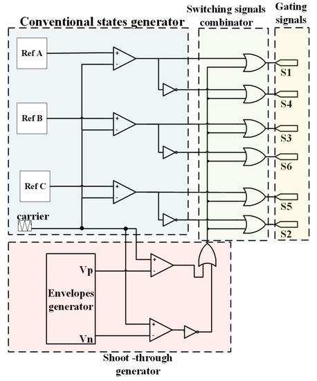
Figure 2.
General signal generator block diagram for three-phase ZSI carrier-based PWM techniques.
Simple Boost PWM (SBPWM) was the first proposed PWM technique to control ZSI’s output voltage. It adds two fixed envelopes to the SPWM with magnitudes equal to or greater than the modulation index. However, to reduce voltage stresses, the envelopes magnitude is limited to the modulation index value, as shown in Figure 3a [11].
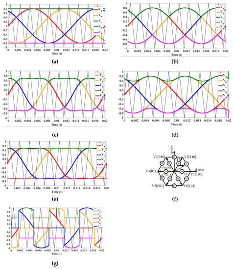
Figure 3.
Three-phase ZSI PWM modulation schemes for: (a) SBPWM, (b) MBPWM, (c) MBPWM with the third harmonic injection, (d) CBPWM, (e) CBPWM with the third harmonic injection, (f) d-q representation of MSVPWM; at Modulation index (M = 0.8), fundamental frequency (f = 50 Hz), (g) ZSI-DCPWM at Modulation index (M = ), fundamental frequency (f = 50 Hz), DC-offset (K = 0.5).
Maximum Boost PWM (MBPWM) uses the instantaneous maximum and instantaneous minimum of the three phase references as the upper and lower envelopes, as shown in Figure 3b, turning all zero states into a shoot-through state. Consequently, the boosting factor is maximized for a wide range of modulation index variations, which causes a large reduction in voltage stresses [51]. However, due to the unfixed envelopes’ difference over one cycle of the fundamental frequency, higher-magnitude low-frequency voltage ripples are remarkable across the DC-link voltage with a frequency equal to six times the output fundamental frequency, increasing the impedance network cost and size.
MBPWM with a third harmonic injection can be utilized to extend the modulation index range of operation up to (), as illustrated in Figure 3c [51].
Constant Boost PWM (CBPWM) features two variable envelopes with a fixed-level difference, leading to low DC-link voltage ripples with reasonable voltage stresses, as shown in Figure 3d. CBPWM with third harmonic injection can be used to simplify the envelopes’ generation and extend the control region up to (M = ), as shown in Figure 3e [52].
Modified space vector PWM (MSVPWM) reshapes conventional SVPWM by inserting the shoot-through state with a time ( inside conventional zero states. The shoot-through state must be distributed around active states to reduce %THD and switching losses, keeping in mind that the active states time is untouchable, as shown in Figure 3g [53,54]. MSVPWM has a wide range of operations with relatively smoother relations and lower stresses compared to SBPWM.
Recently, in late 2016, a discontinuous PWM technique for three-phase ZSI (ZSI-DCPWM) was introduced, achieving a separation between the boosting factor and the modulation index, as shown in Figure 3f [57]. The ZSI-DCPWM technique offers an extended stable range of operation, low sensitivity for variation of control gain, a higher degree of freedom for control variables, moderate voltage stress and reduced %THD at high-gain points.
3. Proposed Modified Discontinuous ZSI-PWM Techniques
ZSI-DCPWM utilizes discontinuous references that can be expressed as [57]
where (, ) are the three-phase references
and ) is a zero-sequence component; the added zero sequence term equals [57]:
where “sgn” is the sign function which yields “1” for positive values and “−1” for negative values. The upper and lower envelopes are extracted from the instantaneous maximum and minimum of the generated references, respectively. To control the boosting factor of ZSI-DCPWM, A DC-offset (K) is used to shift the zero periods of the upper and lower envelopes up/down, leading to shoot-through time decrease/increase. The references’ magnitude has a maximum allowable value of to prevent over-modulation [57].
The proposed modified ZSI-DCPWM (MDCPWM) targets to increase the level of the modulation index without over-modulating the references. This increment is expected to reduce voltage stresses, improve %THD, offer more stable, less sensitive linear voltage gain variation with a wider range of operation and lower sensitivity. In order to extend the modulation index, a third harmonic component is proposed to be added to the generated references hence increasing the maximum allowable modulation index by 15% of its original value to be . The proposed references are
where ( is the third harmonic component with the proposed equation:
Figure 4 illustrates the reference signals for both the conventional and the proposed modified ZSI-DCPWM. It must be noted that the instantaneous difference between any two references is a pure sinusoidal waveform, representing the line voltage, as shown in Figure 4 for both the conventional and proposed ZSI-DCPWM.
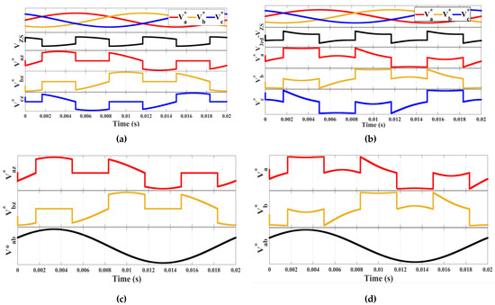
Figure 4.
ZSI-DCPWM references: (a) Conventional ZSI-DCPWM references generation, (b) Proposed Modified DCPWM references generation, (c) Conventional ZSI-DCPWM line voltage, and (d) Proposed Modified DCPWM line voltage.
Extracting the instantaneous maximum and minimum values of the generated references was performed to generate the upper and lower envelopes ( respectively. The boosting factor is controlled by shifting the shaded area shown in Figure 5b up or down with offset value (K) without changing the modulation index value.
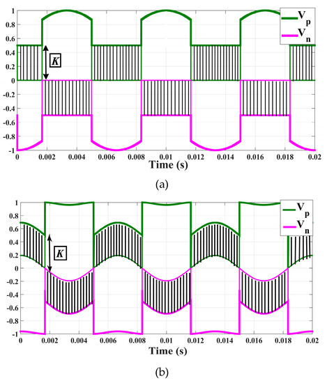
Figure 5.
ZSI-DCPWM envelopes: (a) Conventional ZSI-DCPWM envelopes, (b) Proposed modified DCPWM envelopes.
4. Mathematical Analysis of the Proposed Modified Discontinuous ZSI-PWM Techniques
To obtain the boosting factor, voltage gain and voltage stresses equations of the proposed modified ZSI-DCPWM technique (MDCPWM), the average shoot-through duty ratio was obtained with the help of Figure 6, since the shoot-through duty ratio is a periodic function repeating itself every (), as shown in Figure 6a.
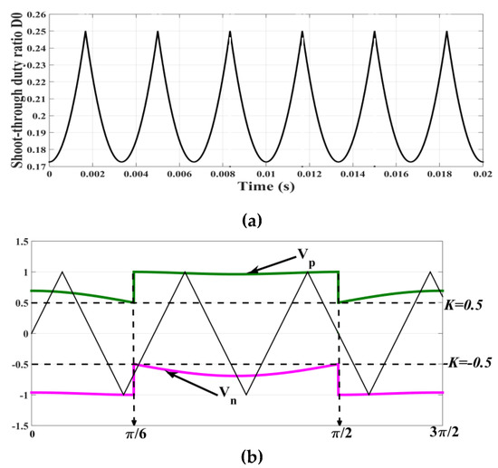
Figure 6.
Proposed modified ZSI-DCPWM shoot-through duty ratio: (a) over one fundamental period at f = 50 Hz and K = 0.5, (b) Upper and lower envelopes during interval (), k = 0.5.
The shoot-through duty ratio during the interval is expressed as
where and are the upper and lower envelopes, respectively, in the interval ().
Then,
The average shoot-through duty ratio over the interval () is
Consequently, the boosting factor (B) is obtained as follows:
The overall voltage gain (G) can be calculated as
Equation (14) describes the voltage gain of the proposed modified ZSI-DCPWM technique, which is the same equation as the conventional ZSI-DCPWM voltage gain [57]. However, the proposed technique can operate at a higher modulation index, with maximum modulation index being extended to (M = ).
The increment in the modulation index causes a reduction in the voltage stresses by 15% less than conventional ZSI-DCPWM voltage stresses:
Figure 7a shows the voltage gain behavior of the proposed modified ZSI-DCPWM compared to conventional ZSI-PWM techniques. The proposed modified ZSI-DCPWM exhibits more linear stable relations at high-gain points. Moreover, Figure 7b,c illustrate a comparison between the performance of each the conventional ZSI-DCPWM and the proposed modified ZSI-DCPWM at different modulation indices.
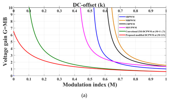
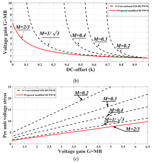
Figure 7.
Comparison between various ZSI PWM techniques: (a) voltage gain behavior for various PWM techniques, (b) voltage gain for conventional and proposed modified DCPWM at different modulation indices, (c) per unit voltage stress for conventional and proposed DCPWM at different modulation indices.
Table 1 gives a breakdown of the governing equations for the proposed and conventional PWM techniques.

Table 1.
ZSI modulation techniques relations.
5. Simulation Analysis
In this section, extensive simulation studies are carried out using the MATLAB/SIMULINK ® software package to verify the theoretical principle of the proposed modified ZSI-DCPWM technique. The simulated model has the same parameters as shown in Table 2.
Table 2.
Simulation parameters.
The target of the simulated model is to produce three-phase line voltage of 60 Vrms. The input to this module is 30 V DC. The required gain for this system is G = 3.3. Using (15), the corresponding offset must be (K = 0.1015).
Figure 8 illustrates the simulation results of the investigated ZSI with the parameters listed in Table 2. At K = 0.1015, the expected gain of 3.3 is validated, as shown in Figure 8a, where the DC-link voltage achieves a value of 150 V from a 30 VDC input. Figure 8b shows that the Z-network inductor current oscillates at a frequency equal to six times the output fundamental frequency. For illustration purposes, the ZSI output voltage is filtered as shown in Figure 8c, showing the fundamental phase and line voltages. Figure 8d illustrates the output line voltage as a pure sinusoidal wave due to the inductive nature of the load impedance. In order to effectively illustrate the superiority of the proposed technique, a comparison is carried out with all the conventional ZSI PWM techniques stated in the literature. Specific benchmarks are tracked to test the ZSI performance under the investigated PWM techniques, mainly, voltage gain, converter switches, voltage stress and %THD. The system performance is simulated at a wide range of gain variations to examine the range of stability as well. Figure 9a shows that for conventional PWM techniques, lower values of modulation index exert a sudden increase in the voltage gain with limited allowable modulation index variation. Among all the investigated ZSI PWM techniques, the third harmonic injection is applicable for MBPWM and CBPWM, which extends the modulation index beyond unity without violating the over-modulation restriction. However, MBPWM offers the most limited allowable modulation index variation. In contrast, the proposed modified ZSI-DCPWM technique provides the widest operating range with a smoother relation between voltage gain and the control gain (K), with the privilege of stable operation even for zero control gain (K = 0), where the maximum obtainable voltage gain is limited to (G = 6.5). Regarding the voltage stress aspect, it can be concluded from Figure 9b,c that for voltage gain (G < 2), the proposed modified ZSI-DCPWM technique has a moderate voltage stresses lower than the conventional ZSI-DCPWM stresses and higher than other conventional techniques stresses, while for voltage gain (2 < G < 4.3), the proposed technique voltage stress is lower than (conventional ZSI-DCPWM, MSVPWM and SBPWM) voltage stress, and voltage gain (4.3 < G < 6.5). The proposed technique has lower stresses than all other PWM control techniques except for MBPWM. However, at (G = 6.5), the voltage stresses of both MBPWM and the proposed technique are equal. Figure 9d illustrates the steady-state voltage ripples across the Z-network capacitor, which is minimized for both SBPWM and CBPWM due to the fixed shoot-through duty ratio. For MBPWM, MSVPWM, conventional ZSI-DCPWM and the proposed modified ZSI-DCPWM techniques, capacitor voltage ripples are high due to the variable shoot-through duty ratio over one fundamental cycle, which increases the Z-network cost and size. Exploring the variation of the %THD in Figure 9e,f, harmonic distortion of conventional PWM techniques is dependent on voltage gain variation as well as the %THD, which is increased for high-gain requirements. ZSI-DCPWM strategies show a unique ability of fixed %THD regardless of the required gain which reduces filter effort. For a wide range of modulation index variations (from 0 to 0.65), the proposed modified ZSI-DCPWM shows the lowest %THD among the investigated ZSI PWM techniques.
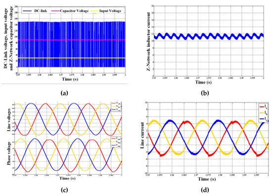
Figure 8.
Simulation results of the proposed modified ZSI-DCPWM: (a) DC side voltages, (b) Z-network inductor current, (c) Output line and phase voltages, (d) Output line currents.
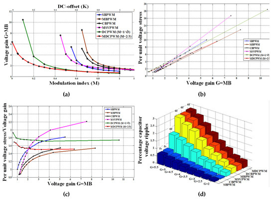
Figure 9.
Simulation-based comparison between the discussed PWM control techniques: (a) Voltage gain versus modulation index (M), DC-offset (K) for conventional and ZSI-DCPWM techniques respectively, (b) per-unit voltage stress versus voltage gain, (c) per unit voltage stresses/voltage gain versus voltage gain, (d) percentage capacitor voltage ripples for the discussed and the proposed ZSI PWM techniques at different gain points (e)%THD versus control variable (M), (K) and (f) %THD versus voltage gain.
6. Experimental Validation
An experimental prototype was built with the same simulation parameters as those shown in Table 2, with two values of load impedance: = 50 Ω (pure resistive) and = 50 + j95 Ω (highly inductive). The PWM control signals with the shoot-through states were generated by high-performance DSP TMS320F28335 Delfino ™ Texas Instruments. The hardware implementation is shown in Figure 10.
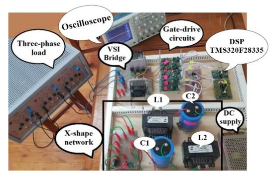
Figure 10.
X-shaped impedance source inverter test reg.
The proposed modified ZSI-DCPWM technique was tested by setting the gain point to produce an output line voltage of 60 Vrms from an input of 30VDC. The required gain was G = 3.3 and the equivalent offset K = 0.1015, while the modulation index is constant at (M = ). For a pure resistive load = 50 Ω, the DC side voltages are shown in Figure 11a, where the input voltage is boosted from 30 V to 150 V across the inverter bridge. Figure 11b illustrates the Z-network inductor current, which oscillates with a frequency equal to six times the fundamental frequency due to shoot-through variation of the proposed modified ZSI-DCPWM. Figure 11c,d shows the output line and phase voltage with the achieved RMS value, while Figure 11e shows the output line current. Figure 11f illustrates output three-phase voltages.
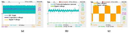
Figure 11.
Experimental results outpt waveforms for the proposed modified ZSI-DCPWM with resistive load = 50 Ω: (a) DC side voltages (input, Capacitor and DC Link voltages), (b) inductor current, (c) line voltage, (d) phase voltage, (e) line current, (f) three-phase voltages.
The same gain point was tested with highly inductive load impedance . The load filters the output line current as shown in Figure 12 to be a near-sinusoid.
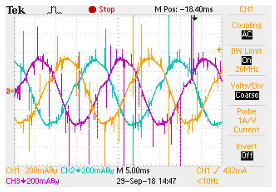
Figure 12.
Experimental output three-phase line current for modified ZSI-DCPWM with highly inductive load = 50 + j95 Ω.
To validate the proposed modified ZSI-DCPWM technique performance, simulation results were experimentally compared to conventional PWM techniques, as shown in Figure 13.
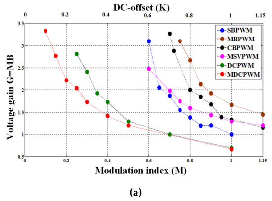
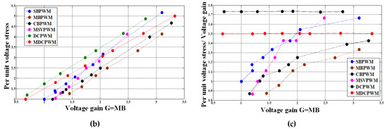
Figure 13.
Experimental performance comparison for the investigated PWM techniques: (a) voltage gain versus control variable (M or K), (b) per-unit voltage stresses versus voltage gain and (c) per unit voltage stress/voltage gain versus voltage gain.
The voltage gain variation with the control variable, modulation index (M) or offset (K) and the inverter switches voltage stresses are the main aspects considered in this comparison. The first aspect gives the scope of the applicability of the PWM technique in various operating regions, while the second one focuses on how much the inverter voltage rating should be enlarged for a wide range of operations. A comparison between the investigated ZSI PWM techniques is presented based on the experimental data results obtained. Figure 13a illustrates the voltage gain for a given modulation index (M) or envelopes offset (K) for the conventional and the proposed modified ZSI-DCPWM techniques, respectively.
It has been noted that the proposed modified ZSI-DCPWM has the privilege of the smoothest relation, which allows for acquiring a high voltage gain without the fear of sudden over voltage stresses. On the other hand, MBPWM has the steepest relation for voltage gain variation, which reduces the control region to be limited within modulation indices (M = 0.75 to M = 1.15). Furthermore, MBPWM, CBPWM and MSVPWM offer an extended modulation index up to (M = 1.15), while SBPWM modulation index is limited to only unity. Moreover, the conventional ZSI-DCPWM and the proposed modified ZSI-DCPWM have a limited modulation index below (M = ) and (M = ) respectively.
Figure 13b,c highlights a comparison between the investigated modulation techniques regarding voltage stresses across the switches. It can be seen that the proposed modified ZSI-DCPWM has moderate voltage stresses compared to other techniques, especially for high-gain points, where it becomes the third lowest in voltage stresses after MBPWM and CBPWM. Moreover, it must be pointed out that both DCPWM-based techniques have constant voltage stresses per voltage gain for a wide range of voltage gain variation due to the merit of the separation between the modulation index and the boosting factor.
7. Conclusions
Z-source inverters can be considered as a promising solution for grid/islanded RES with the privilege of voltage buck/boost capabilities via single-stage conversion. This paper presents a modified discontinuous PWM (MDCPWM) technique for three-phase Z-source inverters. Rigorous simulation results in addition to experimental validation were utilized to illustrate the superior performance of the proposed technique over the entire operating range, comparing it to all the available PWM techniques dedicated to a Z-source inverter. The presented technique offers a smooth voltage gain variation, avoiding undesired steep response at low modulation indices. The proposed MDCPWM technique offers fixed THD over the entire range of operation. In addition, minimized voltage stress can be achieved under the proposed MDCPWM technique for a wide range of operations.
Author Contributions
Conceptualization, A.A.H., A.K.A. and B.W.W.; Data curation, A.A.I.; Formal analysis, A.A.I.; Methodology, A.K.A.; Software, A.A.I.; Supervision, A.A.H. and A.K.A.; Validation, A.A.I.; Writing—review & editing, A.K.A. and B.W.W. All authors have read and agreed to the published version of the manuscript.
Funding
This research received no external funding.
Conflicts of Interest
The authors declare no conflict of interest.
References
- Yaosuo, X.; Liuchen, C.; Baekhj, K.S.; Bordonau, J.; Shimizu, T. Topologies of single-phase inverters for small distributed power generators: An overview. IEEE Trans. Power Electron. 2004, 19, 1305–1314. [Google Scholar]
- Chen, L.; Amirahmadi, A.; Zhang, Q.; Kutkut, N.; Batarseh, I. Design and Implementation of Three-Phase Two-Stage Grid-Connected Module Integrated Converter. IEEE Trans. Power Electron. 2014, 29, 3881–3892. [Google Scholar] [CrossRef]
- Islam, M.R.; Guo, Y.; Zhu, J. A High-Frequency Link Multilevel Cascaded Medium-Voltage Converter for Direct Grid Integration of Renewable Energy Systems. IEEE Trans. Power Electron. 2014, 29, 4167–4182. [Google Scholar] [CrossRef]
- Prasanna, U.R.; Rathore, A.K. Dual Three-Pulse Modulation-Based High-Frequency Pulsating DC Link Two-Stage Three-Phase Inverter for Electric/Hybrid/Fuel Cell Vehicles Applications. IEEE J. Emerg. Sel. Top. Power Electron. 2014, 2, 477–486. [Google Scholar] [CrossRef]
- Debnath, D.; Chatterjee, K. Two-Stage Solar Photovoltaic-Based Stand-Alone Scheme Having Battery as Energy Storage Element for Rural Deployment. IEEE Trans. Ind. Electron. 2015, 62, 4148–4157. [Google Scholar] [CrossRef]
- Wang, Y.F.; Xue, L.K.; Wang, C.S.; Wang, P.; Li, W. Interleaved High-Conversion-Ratio Bidirectional DC–DC Converter for Distributed Energy-Storage Systems—Circuit Generation, Analysis, and Design. IEEE Trans. Power Electron. 2016, 31, 5547–5561. [Google Scholar] [CrossRef]
- Kjaer, S.B.; Pedersen, J.K.; Blaabjerg, F. A review of single-phase grid-connected inverters for photovoltaic modules. IEEE Trans. Ind. Appl. 2005, 41, 1292–1306. [Google Scholar] [CrossRef]
- Dong, D.; Luo, F.; Zhang, X.; Boroyevich, D.; Mattavelli, P. Grid-Interface BidirectiGrid-Interface Bidirectional Converter for Residential DC Distribution Systems—Part One: High-Density Two-Stage Topology. IEEE Trans. Power Electron. 2013, 28, 1667–1679. [Google Scholar] [CrossRef]
- Caceres, R.O.; Barbi, I. A boost DC-AC converter: Analysis, design, and experimentation. IEEE Trans. Power Electron. 1999, 14, 134–141. [Google Scholar] [CrossRef]
- Sanchis, P.; Ursaea, A.; Gubia, E.; Marroyo, L. Boost DC-AC inverter: A new control strategy. IEEE Trans. Power Electron. 2005, 20, 343–353. [Google Scholar] [CrossRef]
- Zheng, P.F. Z-source inverter. IEEE Trans. Ind. Appl. 2003, 39, 504–510. [Google Scholar] [CrossRef]
- Nguyen, M.K.; Jung, Y.G.; Lim, Y.C. Single-Phase AC–AC Converter Based on Quasi-Z-Source Topology. IEEE Trans. Power Electron. 2010, 25, 2200–2210. [Google Scholar] [CrossRef]
- Peng, F.X.; Ming, Q.Z.; Zheng, P.F. Single-phase Z-source PWM AC-AC converters. IEEE Power Electron. Lett. 2005, 3, 121–124. [Google Scholar]
- Tang, Y.; Xie, S.; Zhang, C. Z-source ac–ac converters solving commutation problem. IEEE Trans. Power Electron. 2007, 22, 2146–2154. [Google Scholar] [CrossRef]
- He, L.; Duan, S.; Peng, F. Safe-commutation strategy for the novel family of quasi-Z-source AC–AC converter. IEEE Trans. Ind. Inform. 2013, 9, 1538–1547. [Google Scholar]
- Ahmed, H.F.; Cha, H.; Khan, A.A.; Kim, H.G. A Family of High-Frequency Isolated Single-Phase Z-Source AC–AC Converters with Safe-Commutation Strategy. IEEE Trans. Electron. 2016, 31, 7522–7533. [Google Scholar] [CrossRef]
- Evran, F.; Aydemir, M.T. Isolated High Step-Up DC–DC Converter with Low Voltage Stress. IEEE Trans. Power Electron. 2014, 29, 3591–3603. [Google Scholar] [CrossRef]
- Siwakoti, Y.P.; Loh, P.C.; Blaabjerg, F.; Town, G. Y-source impedance network. 2014 IEEE Applied Power Electronics Conference and Exposition—APEC 2014. IEEE Trans. Power Electron. 2014, 29, 3362–3366. [Google Scholar]
- Zhao, B.; Yu, Q.; Leng, Z.; Chen, X. Switched Z-Source Isolated Bidirectional DC–DC Converter and Its Phase-Shifting Shoot-Through Bivariate Coordinated Control Strategy. IEEE Trans. Ind. Electron. 2012, 59, 4657–4670. [Google Scholar] [CrossRef]
- Vinnikov, D.; Roasto, I.; Strzelecki, R.; Adamowicz, M. Step-Up DC/DC Converters with Cascaded Quasi-Z-Source Network. IEEE Trans. Ind. Electron. 2012, 59, 3727–3736. [Google Scholar] [CrossRef]
- Lei, Q.; Yang, S.; Peng, F.Z.; Inoshita, R. Steady state and transient analysis of a three phase current-fed Z-source PWM rectifier. In Proceedings of the 2009 IEEE Vehicle Power and Propulsion Conference, Dearborn, MI, USA, 7–10 September 2009; pp. 426–432. [Google Scholar]
- Qin, L.; Shuitao, Y.; Peng, F.Z.; Inoshita, R. Three phase current-fed Z-source PWM rectifier. In Proceedings of the 2009 IEEE Energy Conversion Congress and Exposition, San Jose, CA, USA, 20–24 September 2009; pp. 1569–1574. [Google Scholar]
- Ding, X.; Qian, Z.; Xie, Y.; Peng, F.Z. A novel ZVS Z-source rectifier. In Proceedings of the Twenty-First Annual IEEE Applied Power Electronics Conference and Exposition 2006 APEC’06, Dallas, TX, USA, 19–23 March 2006; p. 5. [Google Scholar]
- Kala-Konga, C.L.; Gitau, M.N.; Bansal, R.C. Steady-state and small-signal models of a three-phase quasi-Z-source AC–DC converter for wind applications. IET Renew. Power Gener. 2016, 10, 1033–1040. [Google Scholar] [CrossRef]
- Xu, H.; Peng, F.Z.; Chen, L.; Wen, X. Analysis and design of Bi-directional Z-source inverter for electrical vehicles. In Proceedings of the 2008 Twenty-Third Annual IEEE Applied Power Electronics Conference and Exposition, Austin, TX, USA, 24–28 February 2008; pp. 1252–1257. [Google Scholar]
- Anderson, J.; Peng, F.Z. Four quasi-Z-Source inverters. In Proceedings of the 2008 IEEE Power Electronics Specialists Conference, Rhodes, Greece, 15–19 June 2008; pp. 2743–2749. [Google Scholar]
- Gajanayake, C.J.; Luo, F.L.; Gooi, H.B.; So, P.L.; Siow, L.K. Extended-Boost Z-Source Inverters. IEEE Trans. Power Electron. 2010, 25, 2642–2652. [Google Scholar] [CrossRef]
- Zhu, M.; Yu, K.; Luo, F.L. Switched Inductor Z-Source Inverter. IEEE Trans. Power Electron. 2010, 25, 2150–2158. [Google Scholar]
- Nguyen, M.K.; Lim, Y.C.; Cho, G.B. Switched-Inductor Quasi-Z-Source Inverter. IEEE Trans. Power Electron. 2011, 26, 3183–3191. [Google Scholar] [CrossRef]
- Ahmed, H.F.; Cha, H.; Kim, S.H.; Kim, H.G. Switched-Coupled-Inductor Quasi-Z-Source Inverter. IEEE Trans. Power Electron. 2016, 31, 1241–1254. [Google Scholar] [CrossRef]
- Loh, P.C.; Li, D.; Blaabjerg, F. Γ-Z-Source Inverters. IEEE Trans. Power Electron. 2013, 28, 4880–4884. [Google Scholar] [CrossRef]
- Nguyen, M.K.; Lim, Y.C.; Kim, Y.G. TZ-source inverters. IEEE Trans. Ind. Electron. 2013, 60, 5686–5695. [Google Scholar] [CrossRef]
- Qian, W.; Peng, F.Z.; Cha, H. Trans-Z-Source Inverters. IEEE Trans. Power Electron. 2011, 26, 3453–3463. [Google Scholar] [CrossRef]
- Hossam-Eldin, A.; Abdelsalam, A.K.; Refaey, M.; Ali, A.A. A topological review on recent improvements of three-phase impedance source inverter. In Proceedings of the 2017 Nineteenth International Middle East Power Systems Conference (MEPCON), Cairo, Egypt, 19–21 December 2017; pp. 1106–1112. [Google Scholar]
- Shen, M.; Joseph, A.; Wang, J.; Peng, F.Z.; Adams, D.J. Comparison of Traditional Inverters and Z -Source Inverter for Fuel Cell Vehicles. IEEE Trans. Power Electron. 2007, 22, 1453–1463. [Google Scholar] [CrossRef]
- Guo, F.; Fu, L.; Lin, C.H.; Li, C.; Choi, W.; Wang, J. Development of an 85-kW Bidirectional Quasi-Z-Source Inverter with DC-Link Feed-Forward Compensation for Electric Vehicle Applications. IEEE Trans. Power Electron. 2013, 28, 5477–5488. [Google Scholar] [CrossRef]
- Peng, F.Z.; Shen, M.; Holland, K. Application of Z-Source Inverter for Traction Drive of Fuel Cell—Battery Hybrid Electric Vehicles. IEEE Trans. Power Electron. 2007, 22, 1054–1061. [Google Scholar] [CrossRef]
- Battiston, A.; Miliani, E.H.; Pierfederici, S.; Meibody-Tabar, F. Efficiency Improvement of a Quasi-Z-Source Inverter-Fed Permanent-Magnet Synchronous Machine-Based Electric Vehicle. IEEE Trans. Transp. Electrif. 2016, 2, 14–23. [Google Scholar] [CrossRef]
- Dehghan, S.M.; Mohamadian, M.; Yazdian, A. Hybrid Electric Vehicle Based on Bidirectional Z-Source Nine-Switch Inverter. IEEE Trans. Veh. Technol. 2010, 59, 2641–2653. [Google Scholar] [CrossRef]
- Liu, P.; Liu, H.P. Permanent-magnet synchronous motor drive system for electric vehicles using bidirectional z-source inverter. IET Electr. Syst. Transp. 2012, 2, 178–185. [Google Scholar] [CrossRef]
- Li, Y.; Jiang, S.; Cintron-Rivera, J.G.; Peng, F.Z. Modeling and Control of Quasi-Z-Source Inverter for Distributed Generation Applications. IEEE Trans. Ind. Electron. 2013, 60, 1532–1541. [Google Scholar] [CrossRef]
- Ge, B.; Abu-Rub, H.; Peng, F.Z.; Lei, Q.; De Almeida, A.T.; Ferreira, F.J.; Sun, D.; Liu, Y. An Energy-Stored Quasi-Z-Source Inverter for Application to Photovoltaic Power System. IEEE Trans. Ind. Electron. 2013, 60, 4468–4481. [Google Scholar] [CrossRef]
- Abu-Rub, H.; Iqbal, A.; Ahmed, S.M.; Peng, F.Z.; Li, Y.; Baoming, G. Quasi-Z-Source Inverter-Based Photovoltaic Generation System with Maximum Power Tracking Control Using ANFIS. IEEE Trans. Sustain. Energy 2013, 4, 11–20. [Google Scholar] [CrossRef]
- Gajanayake, C.J.; Vilathgamuwa, D.M.; Loh, P.C.; Teodorescu, R.; Blaabjerg, F. Z-Source-Inverter-Based Flexible Distributed Generation System Solution for Grid Power Quality Improvement. IEEE Trans. Energy Convers. 2009, 24, 695–704. [Google Scholar] [CrossRef]
- Noroozi, N.; Zolghadri, M.R. Three-Phase Quasi-Z-Source Inverter with Constant Common-Mode Voltage for Photovoltaic Application. IEEE Trans. Ind. Electron. 2017, 65, 4790–4798. [Google Scholar] [CrossRef]
- Sajadian, S.; Ahmadi, R. Model Predictive-Based Maximum Power Point Tracking for Grid-Tied Photovoltaic Applications Using aZ-Source Inverter. IEEE Trans. Power Electron. 2016, 31, 7611–7620. [Google Scholar] [CrossRef]
- Liu, J.; Jiang, S.; Cao, D.; Peng, F.Z. A Digital Current Control of Quasi-Z-Source Inverter with Battery. IEEE Trans. Ind. Inform. 2013, 9, 928–937. [Google Scholar] [CrossRef]
- Navas, M.A.H.; G, F.L.; Puma, J.L.A.; A, J.A.T.; Filho, A.J.S. Battery Energy Storage System Applied to Wind Power System Based On Z-Source Inverter Connected to Grid. IEEE Lat. Am. Trans. 2016, 14, 4035–4042. [Google Scholar] [CrossRef]
- Zhou, Z.J.; Zhang, X.; Xu, P.; Shen, W.X. Single-Phase Uninterruptible Power Supply Based on Z-Source Inverter. IEEE Trans. Ind. Electron. 2008, 55, 2997–3004. [Google Scholar] [CrossRef]
- Shahparasti, M.; Yazdian, A.; Mohamadian, M.; Larijani, A.S.; Fatemi, A. Parallel uninterruptible power supplies based on Z-source inverters. IET Power Electron. 2012, 5, 1359–1366. [Google Scholar] [CrossRef]
- Zheng, P.F.; Miaosen, S.; Zhaoming, Q. Maximum boost control of the Z-source inverter. IEEE Trans. Power Electron. 2005, 20, 833–838. [Google Scholar]
- Miaosen, S.; Jin, W.; Joseph, A.; Zheng, P.F.; Tolbert, L.M.; Adams, D.J. Constant boost control of the Z-source inverter to minimize current ripple and voltage stress. IEEE Trans. Ind. Appl. 2006, 42, 770–778. [Google Scholar] [CrossRef]
- Rostami, H.; Khaburi, D.A. A new method for minimizing of voltage stress across devices in Z-source inverter. In Proceedings of the 2011 2nd Power Electronics, Drive Systems and Technologies Conference (PEDSTC), Tehran, Iran, 16–17 February 2011; pp. 610–614. [Google Scholar]
- Jung, J.W.; Keyhani, A. Control of a Fuel Cell Based Z-Source Converter. IEEE Trans. Energy Convers. 2007, 22, 467–476. [Google Scholar] [CrossRef]
- Agelidis, V.G.; Ziogas, P.; Joos, G. Dead-band’ PWM switching patterns. In Proceedings of the PESC ‘92 Record 23rd Annual IEEE Power Electronics Specialists Conference, Toledo, Spain, 29 June–3 July 1992; Volume 1, pp. 427–434. [Google Scholar]
- Steinke, J.K. Switching frequency optimal PWM control of a three-level inverter. IEEE Trans. Power Electron. 1992, 7, 487–496. [Google Scholar] [CrossRef]
- Diab, M.S.; Elserougi, A.A.; Massoud, A.M.; Abdel-Khalik, A.S.; Ahmed, S. A Pulsewidth Modulation Technique for High-Voltage Gain Operation of Three-Phase Z-Source Inverters. IEEE J. Emerg. Sel. Top. Power Electron. 2016, 4, 521–533. [Google Scholar] [CrossRef]
- Abdelhakim, A.; Blaabjerg, F.; Mattavelli, P. Modulation Schemes of the Three-Phase Impedance Source Inverters—Part I: Classification and Review. IEEE Trans. Ind. Electron. 2018, 65, 6309–6320. [Google Scholar] [CrossRef]
- Bakar, M.S.; Rahim, N.A.; Ghazali, K.H.; Hanafi, A.H.M. Z-source inverter pulse width modulation: A survey. In Proceedings of the International Conference on Electrical, Control and Computer Engineering 2011 (InECCE), Pahang, Malaysia, 21–22 June 2011; pp. 313–316. [Google Scholar]
- Singh, N.; Jain, S.K. A review on modulation techniques of Z-source network. In Proceedings of the 2016 7th India International Conference on Power Electronics (IICPE), Patiala, India, 17–19 November 2016; pp. 1–6. [Google Scholar]


© 2020 by the authors. Licensee MDPI, Basel, Switzerland. This article is an open access article distributed under the terms and conditions of the Creative Commons Attribution (CC BY) license (http://creativecommons.org/licenses/by/4.0/).