1. Introduction
The thermal characterization of power devices and assemblies has become more and more important with the growing level of power density. The related measurements may serve different purposes; they can be used in providing data sheet values, for calibrating thermal models of packaged devices, etc.
In static tests, steady temperature values are measured at certain locations in an assembly. In transient tests, a much larger amount of information can be gained recording the change of the temperature at one or more points over a time period. The two techniques are interrelated; steady state can be reached only through transient events, and transient techniques automatically yield static values when they end.
Transient testing has a deeper theoretical background, presented in References [
1,
2,
3,
4,
5,
6,
7,
8]. Both static and transient techniques are standardized as treated in related References [
9,
10,
11,
12,
13,
14,
15,
16,
17,
18]. Some of the tools used for obtaining simulated and measured results presented in this work are referred to in References [
19,
20,
21].
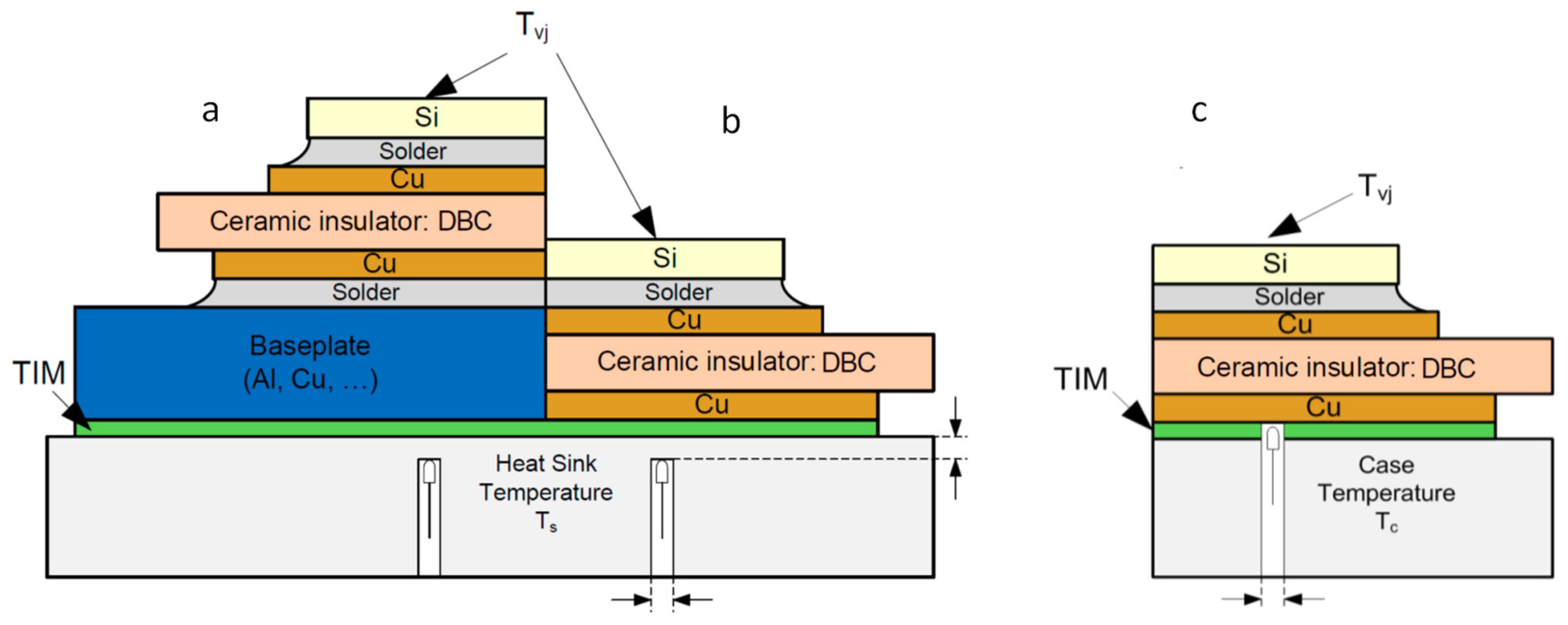
Power devices and the assemblies composed of them are typically sandwich-like structures. The heat generated in silicon chips flows through a complex structure built of different layers of metals, ceramics, solder, and thermal paste (
Figure 1). All layers have different thermal conductance, shear modulus, and other parameters.
In a thermal test, the temperatures are converted, in most cases, to an electric signal, either measuring the temperature-sensitive electric parameters of the semiconductor chips in the assembly or using dedicated sensors at accessible outer points. A suitable sensitive parameter can be the forward voltage of a pn-type junction in a semiconductor device or the thermal voltage induced by the Seebeck effect in metal–metal junctions (i.e., thermocouples).
The recorded thermal quantities are typically distilled into simpler thermal descriptors, sometimes formulated as charts (e.g., Zth plots, structure functions, pulse thermal resistance diagrams) and sometimes into single numbers (junction to ambient, junction to case thermal resistance, etc.).
Based on theoretical considerations, a transient test can yield partial thermal resistances between internal layers of the assembly. As it is shown in detail in References [
4,
5], this way a measurement at a single point can provide information on the temperature of structures which are normally not accessible.
In the electric world, measurements are highly repeatable and remain so when they are reproduced at different laboratories with different instrumentation. For example, voltage measurements yield results of 5 to 7 digits, and different instruments provide the same numbers within a fraction of a percent.
For thermal measurements, this is not the case. In electric measurements, the “conductive” and “insulating” parts of the measurement arrangement differ in their conductivity at a ratio of 1:1012; in thermal tests, this ratio is 1:100. Accordingly, parallel heat flow paths which exist besides the main one can influence the calibration and measurement process. Although it is expected that the thermal tests comply with related standards and actual temperatures can be measured with an accuracy of a few percent, the calculated thermal metrics can be up to 30% different when carried out at a different site with other instruments and thermal environment.
In this study, we first define the thermal quantities which can be measured and the relevant thermal metrics which can be gained from them. Then, we introduce the concept of transient and static thermal tests. Further on, related thermal measurement standards are discussed. Lastly, the reproducibility of thermal parameters measured in different test concepts is examined, and conclusions are drawn.
2. Simple Thermal Metrics: The Junction to Ambient and the Junction to Case Thermal Resistance
Several thermal measurement standards have been defined in order to simplify the description of thermal behavior with single numbers [
9,
10,
11,
12,
13,
14,
15,
16]. Based on the fact that the thermal conductivity of the typical materials used in power packages is nearly constant in the temperature range of their use, these descriptors are often
partial thermal resistances. In a strict treatment, such a partial resistance is interpreted between two isothermal surfaces in an assembly, and they express that the temperature drop between such surfaces is proportional to the heat flux flowing between them. These isothermal surfaces are not accessible in most cases for attaching temperature sensors, and the accessible geometries in the assembly are rarely isothermal. This contradiction can be resolved in many cases using transient characterization techniques as demonstrated in References [
1,
2,
3,
4,
5,
6].
The primary descriptor used for characterizing a full assembly is the RthJA junction to ambient thermal resistance, and the one for a power device with a dedicated cooling surface is the RthJC junction to case thermal resistance. These already give a general impression on the thermal performance of an assembly or a device and can be used for approximate back-of-the envelope calculations.
The context and the interpretation of these metrics slightly differ in various standards, now we use the most consistent approach defined in the JEDEC JESD51 set of standards [
12].
The standard describes the thermal system as a single heat source (junction) where P power is generated, and then a heat flux flows, partly or fully, through reference surfaces which are accessible for temperature probes.
In
Figure 2 we cumulated all threads of the heat flow in a usual power device package structure into a thermal network equivalent. The heat is supposed to be generated at the point J. The part of the material through which the heat flux flows from the junction towards an X reference surface is represented by an
RA thermal resistance; the next part where the flux leaves X towards the ambient is denoted by
RB. A portion of the heat does not flow through X, and the corresponding portion of the assembly is cumulated into
RH.
For the usual cases, when most of the heat flows through X, the standard defines an
RthJX thermal resistance as:
where
TJ is the temperature of the junction and
TX is that of the reference surface. We can observe that in this definition it is tacitly supposed that the temperature distribution on such a reference surface is nearly homogeneous; the geometrical surfaces in the system coincide with isothermal surfaces (which is rarely true).
Of course, at the end, all heat flows towards the ambient. The
RthJA junction to ambient thermal resistance is defined as:
So far, one might think that the best approach is to measure the junction temperature and the temperature of a point on the X surface. Measuring the junction temperature is a challenge in itself as we show later. What is even worse, as it is shown in Reference [
6] and in
Section 6, the errors made in measuring
TJ and
TA can be added up. A more relevant measurement approach is composing the difference in time, rather than in space.
For example, in a junction to ambient measurement one can apply two different power levels,
P1 and
P2, and measure the junction temperature after temperature stabilization in each case. The two measurements yield:
so
This differential principle offers a lot of advantages. The temperature is measured at a single point of the system. As shown later, with this solution all offset problems at measurement and calibration cancel out.
In many cases, the X surface is an exposed cooling surface of a power device or module, the “case”. In the simplest approach, the junction to case thermal resistance can be defined in a two-point measurement, measuring the “temperature of the case”,
TC:
However, the measurement of a “case temperature” is far from being unambiguous, as presented in References [
2,
3,
4,
5,
6] and in
Section 3 and
Section 5 below.
Another way for finding
RthJC is, again, based solely on the change of the junction temperature. This method, called the Transient Dual Interface Measurement (TDIM), compares more complex but more repeatable thermal descriptors, such as the structure functions of a device-on-heat sink arrangement, and defines the junction to case thermal resistance as the point where the structure descriptors start do differ. This methodology is defined among others in the JEDEC JESD 51-14 standard [
13].
It has to be emphasized that the TDIM method yields much more than just a single RthJC value; it automatically generates a one-dimensional thermal compact model of the power device or module.
In real measurements, many factors influence the achievable accuracy of thermal data and of the thermal metrics calculated from them. In order to separate the measurement errors related to the composition of the assembly and the ones caused by the inaccuracies of the test equipment, we present below the results of a simulated experiment and of real tests.
3. Simulation Experiment on Static and Transient Metrics
The errors of thermal measurements have various sources. A bunch of the problems are associated to the transient behavior of the devices under test. Some other problems are related to the instrumentation and to the thermal tester equipment. These problems are investigated in
Section 4.
Another set of inaccuracies is related to the test arrangement. These can be best investigated in a simulation experiment, where the device and instrument induced errors play no role.
For demonstrating the techniques used and the associated problems, we present the temperature changes of specific points in a typical assembly, an IGBT module mounted on a cold plate with various thermal interface material (TIM) layers under the base plate.
In this section, we focus on the measurement problem; for this reason, the actual dimensions, material parameters, and temperature monitor points are presented separately below in
Appendix A (
Table A1 and
Table A2,
Figure A1 and
Figure A2). A simplified sketch of the arrangement is shown in
Figure 3.
The IGBT chips were 11.2 mm × 11.2 mm in size, and this dimension is of interest for treating the displacement-related errors. The layers of the assembly were approximately the ones shown in
Figure 1a. Under the silicon chips, a laminate of solder, copper, and ceramics layers was attached to an aluminum base plate. The cold plate was modelled with a constant heat transfer coefficient (HTC) of 3000 W/m
2K which is a realistic value for an aluminum surface with internal water cooling.
In order to examine the influence of the base plate to cold plate thermal interface, a 50 μm TIM layer was inserted between the module and the cold plate.
In this assembly, the transients were simulated in the FloTHERM tool [
19] at a 100 W power step (heating), uniformly distributed on the die surface.
The monitoring points for the simulated transients were selected as follows:
Ch0: center on the top of the powered semiconductor die, in the dissipating layer;
Ch1: center on the top of the TIM, below the semiconductor die;
Ch2: center on the bottom of the TIM, adjoining the cold plate;
Ch3: as Ch1, but displaced from the center towards the right edge of the die, by 3 mm;
Ch 4: as Ch2, but displaced from the center towards the right edge of the die, by 3 mm.
Obviously, Ch0 corresponds to the junction temperature.
The monitoring point Ch1 mimicked the ideal placement of the thermocouple for measuring the temperature of the “reference point” shown in
Figure 1a. This was also the prescribed position for determining
RthJC in References [
10,
16].
The monitoring point Ch2 corresponded to the case when the probe does not (completely) penetrate the TIM layer. Both Ch3 and Ch4 represented small lateral displacement of the probe, now about half of the chip size, as it mostly happens at such measurements.
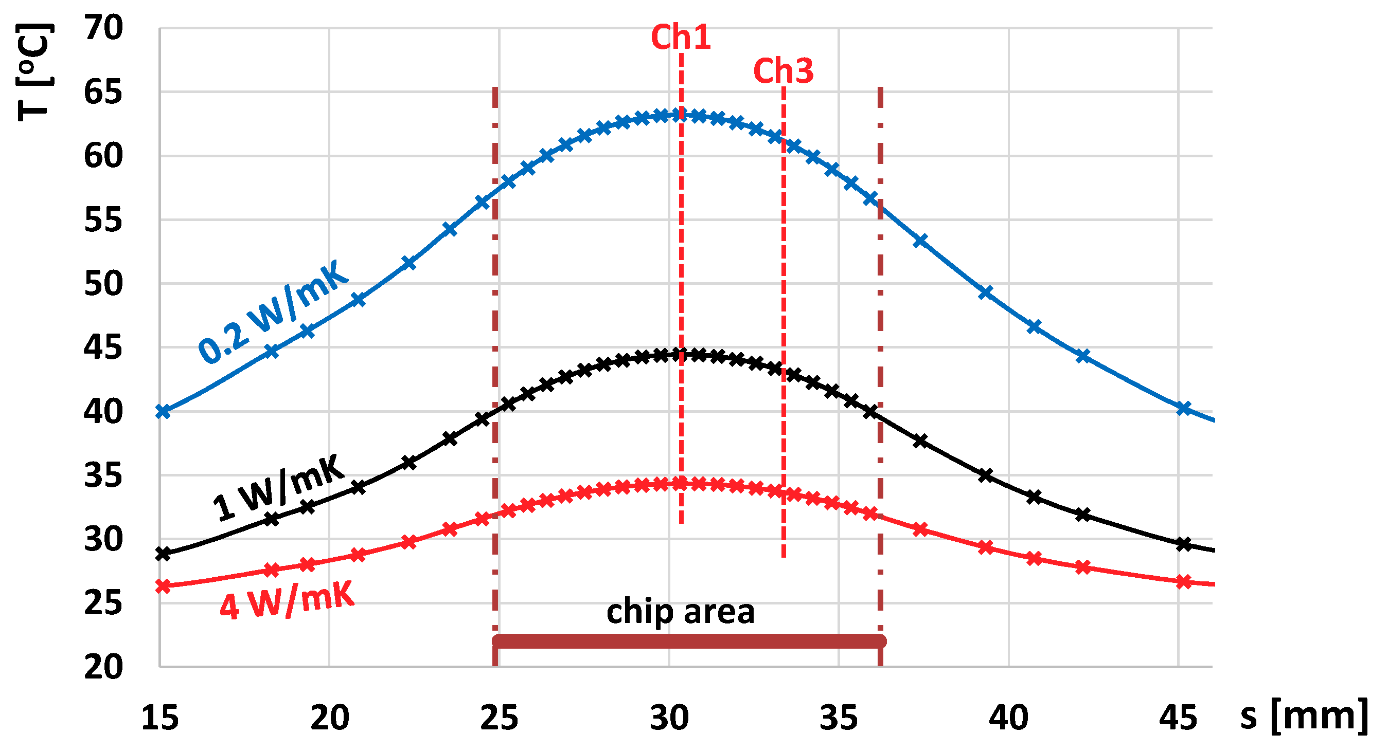
For illustrating different measurement methodologies, the TIM layer was represented by different thermal conductivities, such as dry surface (0.2 W/mK) and different interface materials (1 W/mK, 4 W/mK). The two latter conductivity values corresponded to different qualities of thermal grease materials.
Figure 4 shows the change of temperature at the monitoring points at the different TIM conductivities. Besides the obvious fact that the improved thermal interface reduces the temperature elevation from 50 K to 26 K, the figure also proves that a good TIM also makes it less essential whether the reference probe really touches the module baseplate or it is just “somewhere near” (Ch0–Ch1 versus Ch0–Ch2 distance).
The figure also indicates that the external monitor points reacted on the power change with a 0.5 s delay; accordingly, also in a live system, a slow data acquisition of the reference temperatures with a few samples measured in a second was appropriate. One can observe that more intensive cooling resulted in earlier stabilization of the temperature, and steady state was approximately reached at 140 s, 50 s, and 30 s for the interface layers of 0.2 W/mK, 1 W/mK, and 4 W/mK thermal conductivity, respectively.
It would be hard to provide the full three-dimensional temperature distribution in the assembly as it develops in time;
Figure 4 is restricted to a few characteristic points.
Another informative chart presents the typical bell-shaped temperature distribution of the case_bottom/TIM_top interface in steady state (
Figure 5). The peak temperature under the chip center corresponds to the final transient value at Ch1, shown as a blue “x” marker for the “dry” assembly in
Figure 4a and as black “x” and red “x” markers in
Figure 4b,c, respectively, for different TIM qualities. Note the large temperature difference even within the chip area.
The temperature record in
Figure 4 depicts only the outcome of one certain powering at three given boundaries. The results can be interpreted in a more general way calculating the
Zth thermal impedance curves which are derived normalizing the time-dependent temperature
change by the applied power:
The
Zth curves are popular thermal descriptors of a system. They can be used already for back of the envelope calculations; knowing an actual
Pact heating power in the system, the temperature change in time will be approximately
TJ(
t) =
Pact Zth(
t) +
Tref, where
Tref is the temperature of the whole assembly at low powering. Moreover, further thermal descriptors can be derived from
Zth as shown in References [
1,
5,
13] and in further sections below.
In
Figure 6, we can see the
Zth curves (normalized temperature change) of the arrangement with the three different TIM materials.
With a TIM layer of λ = 0.2 W/mK, first we can observe that the
RthJA total junction to ambient thermal resistance of the assembly is 0.52 K/W. This is the only true physical quantity in such a thermal measurement, based on the objective measured data without further assumptions on locations, divergence threshold, and other artificial elements introduced later on for other thermal metrics. The only approximation is assuming a uniform
TJ junction temperature. Some considerations on the validity of this assumption are given in Reference [
22].
Measuring separately the junction and an external probe yields
RthJC = 0.13 K/W junction to case thermal resistance if the probe penetrates the TIM, and
RthJC = 0.45 K/W if the probe just touches the lower surface of it (“
B = 0–1” and “
A = 0–2” in
Figure 6a, respectively).
With a TIM layer of λ = 1 W/mK, separate measurements at the junction and at the external probe yield
RthJC = 0.16 K/W if the probe penetrates the TIM, and
RthJC = 0.28 K/W if the probe just touches the lower surface of it (“
B = 0–1” and “
A = 0–2” curves in
Figure 6b, respectively). At this TIM quality for the whole assembly,
RthJA is 0.36 K/W.
With a TIM layer of λ = 4 W/mK, the two-point method yields
RthJC = 0.18 K/W junction to case thermal resistance if the probe penetrates the TIM, and
RthJC = 0.19 K/W if the probe just touches the lower surface of it (“
B” and “
A” curves in
Figure 6c, respectively);
RthJA is now 0.28 K/W.
We can observe that, with better TIM and cold plate qualities, the measured junction to case thermal resistance grows as the heat flow is more attracted to the center of the die–die attach–insulator–base plate sandwich, and the base plate temperature is more uniform (
Figure 5). With real thermocouples where the probe tip is coated with an insulator layer and the wires draw some of the heat from the sensor tip, the measured thermal resistance can be well 100% larger than the ideal value obtained in a simulation.
The TDIM methodology is a transient method which is based on measurement at a single point. This technique is based on the comparison of the change of the junction temperature at different boundaries.
Figure 7 compares the
Zth curves belonging to the junction at different TIM qualities. We can observe that the heat flow arrived at the base plate at 1.7 s, and the curves deviated a bit below 0.2 K/W.
This difference is much more expressed in the structure functions which can be derived from the Zth plot of to the hottest point (junction).
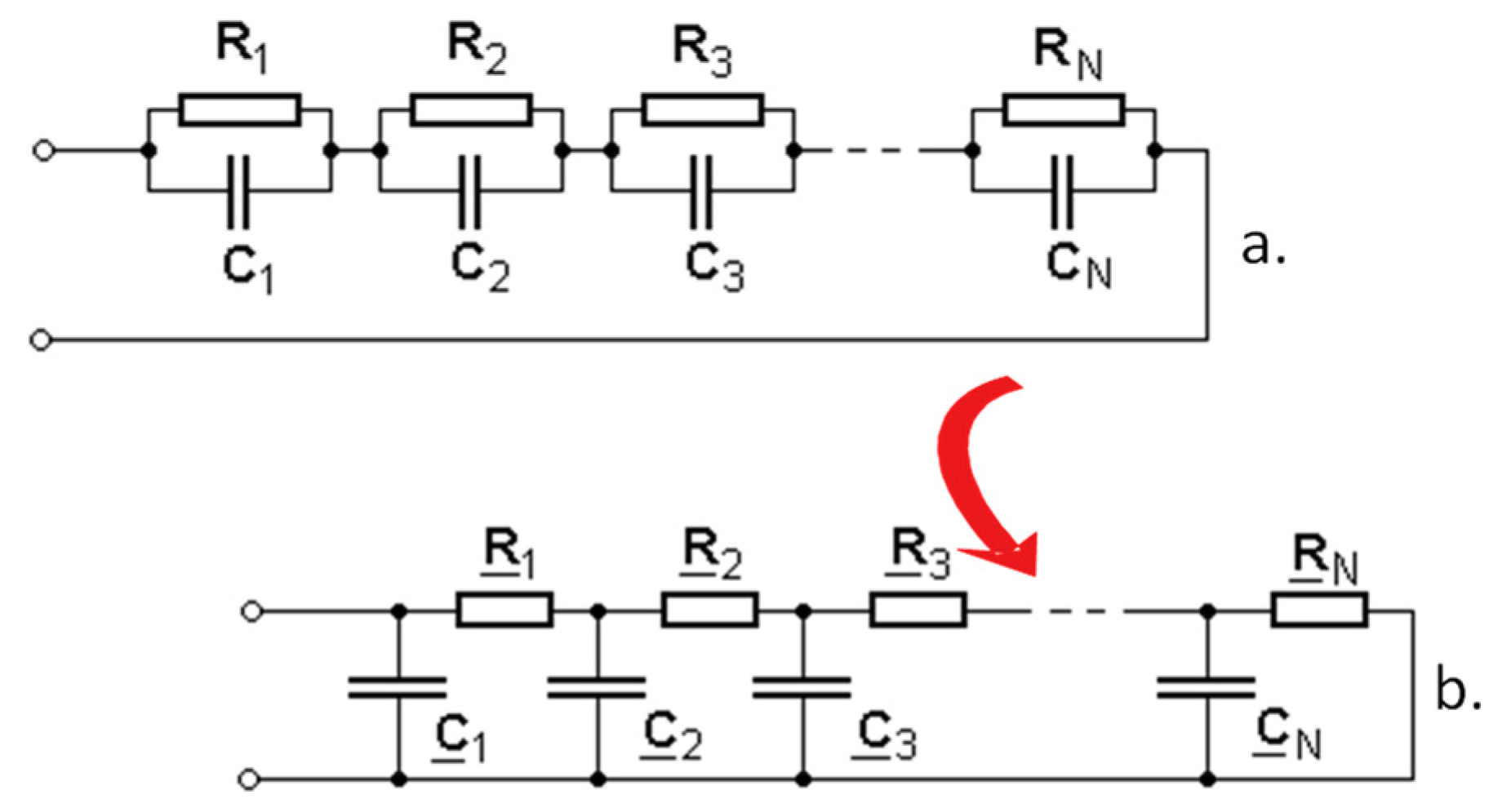
Figure 8a shows the equivalent RC chain circuit of thermal resistances and capacitances which corresponds to the exponential decomposition of the
Zth curves (Foster network). This RC chain can always be converted into a ladder-type network shown in
Figure 8b (Cauer network).
The Foster–Cauer RC transformation is a systematic process of consecutive steps of division and subtraction, presented in detail in Reference [
13]. The theoretical background of the technique is outlined in Reference [
1], and many practical hints on its use are given in References [
2,
3,
4,
5,
6,
7,
8]. Moreover, an interesting treatment of a modified method is presented in Reference [
18].
The Cauer network can be visualized in a structure function (
Figure 9). In this plot, we summed up the thermal resistances in the ladder, starting from the heat source (junction) along the
x-axis and the thermal capacitances along the
y-axis.
Thermal capacitance is proportional to the mass and volume of a material layer through its specific heat and density. Low gradient sections in the chart mean that a small amount of material having low capacitance causes large change in the thermal resistance. These regions have low thermal conductivity or a small cross-sectional area. Steep sections correspond to material regions of high thermal conductivity or a large cross-sectional area, as even a large bulk of material corresponding to high thermal capacitance is of low thermal resistance only. Sudden breaks of the slope belong to material or geometry changes. Thus, thermal resistance and capacitance values, geometrical dimensions, heat transfer coefficients, and material parameters can be directly read on structure functions.
In
Figure 9, the structure functions generated from the
Zth curves of
Figure 7 are compared. The curves belonging to different thermal conductivities started to diverge after 0.17 K/W. Until this point, we see the characteristic steps in the structure function corresponding to the sandwich-like internal structure of the module composed of materials of highly different thermal conductivities.
One can note that the figure also describes well, besides the device under test, also the test fixture and the external cooler. The separation between the device and the outer environment occurs around the RthJC = 0.17 K/W, CthJC = 30 J/K point. Further on, we see the change of the thermal conductivity and specific heat in the external domains of the test equipment.
The approximate thermal capacitances of the components of the material stack are listed in
Table A2. We cropped
Figure 9 above 3000 J/K, as all the lines turn vertical, and no further change in the thermal resistance can be observed. In the case of a real measurement on real cold plate as presented in
Section 4 below, this capacitance would correspond to 700 liters of water, driven through the cold plate of the tester for more than 10 min at typical pump rates, we can rightfully assign this thermal capacitance to the “ambient”.
At this high thermal capacitance, the structure functions end at the RthJA junction to the ambient values (i.e., 0.52 K/W, 0.36 K/W, and 0.28 K/W) established previously.
In the case of real measurements, some noise-induced perturbation occurs on the curves; for this reason, the TDIM measurement, as outlined in the standard [
13], requests an ε threshold to be defined in the thermal capacitance, after which the structure functions can be treated as different.
Figure 10 presents the difference of the structure functions in
Figure 9. The figure demonstrates that selecting a threshold between 0.05 J/K and 2 J/K, being of a ratio of 40, we can state that the
RthJC junction to case thermal resistance is between 0.17 K/W and 0.19 K/W. In real cases with actual measured transients instead of simulated ones, this difference is less steep, as shown in Reference [
23], but still gives a sharp detection of the
RthJC quantity.
The JEDEC JESD51-14 standard defines the details of the TDIM methodology and identifies two alternative metrics by which the divergence point of the measured curves can be quantified. One such metric is the difference in the derivative of the Zth curves, and the other is the difference of structure functions. It has to be noted that both metrics are related to “edge-enhancing” techniques of image processing which are famous also for their noise enhancing nature.
Sources of Uncertainty, According to the Simulation Experiment
As a result of the above presented simulations, we can conclude that when using two-point methodologies for determining the RthJC thermal metrics, the obtained value depends on the TIM quality, lateral displacement of the probe measuring the “case” temperature, penetration of the probe through the TIM, the heat transfer coefficient of the cold plate, and other factors.
In the case of a single-point test, the assembly is totally destroyed and rebuilt between the two measurements. The differences in TIM quality belong to the essence of the technique. Still, although the structure functions are highly reproducible, a decision on the ε threshold used has to be made to define at which divergence point it is considered to be the RthJC value.
In a rigorous simulation model, the temperature transient at Ch2 would be valid only if the probe does not protrude into the TIM layer. This assumption is true when elastomer foils, metal laminates or similar TIMs are used.
If the TIM used is some thermal paste, the probe tip is pressed into it by its elastic support. However, other effects (listed below in
Section 4) would cause a systematically lower recorded temperature in the same way as shown for Ch2 in the simulation experiment.
4. Thermal Transient Tests
In the case of measurements, the consequences of the simulation experiment remain valid, but now inaccuracies of the device characteristics and of the test system have to be considered in addition.
Thermal transient measurements need one or more heater elements and one or several temperature sensors in a system. In most cases, the heat source is a piece of semiconductor, typically called a “chip” in the literature on system design and “die” in works on semiconductor technology and packaging.
Normally, the hottest point in the circuitry is the powered thin material layer of the semiconductors, traditionally called “junction”. For many device categories (diodes, MOSFETs, IGBTs), both the heat source and the sensor are, in fact, pn junctions which are driven into forward operation (
Figure 11). A sudden power change on the junction can be created by
switching down from a high
IH heating current to a low
IM measurement current level.
In actual realizations of the thermal test instruments, IM is realized as a steady source of programmable low I2 current. A programmable high I2 current can be swapped between the device under test and an external shunt; IH is composed as I1 + I2.
First, we demonstrate the basics of the thermal transient testing in an actual test of a power IGBT module. The actual device type and measurement equipment are not the focus of the present study, the description of the test setup, the environment, and photographs are presented again in
Appendix A.
With trial measurements, we found that a relevant test can be carried out at a 50 A heating and 100 mA measurement current.
The measurement current was used in two related steps of the transient testing. In a
calibration process, the forward voltage (or other temperature-sensitive parameter) at
IM was recorded in a thermostat at different
TJ junction temperatures; such a voltage to temperature mapping is provided.
Figure 12 presents the
VCE(
TJ,
IM) calibration curve of the actual device.
The test started with a longer equalization period until the
VCE voltage at constant
IH stabilized. When steady state was reached, the
PH =
VCE(
IH)⋅
IH power on the device was stored, and after switching down to
IM, the change of
VCE(
TJ,
IM) was recorded. During the transient recording there was also a low
PM =
VCE(
IM)⋅
IM power on the device; the Δ
P power step was calculated as the difference of
PH and
PM. We found that the power step on the actual device was around 55 W when switching down from 50 A to 100 mA. The power step slightly depends on the actual thermal boundary which obviously influences
VCE(
TJ,
IH) at the same
IH. Details of the switching process are presented in Reference [
4].
Figure 13 presents the change in the saturation voltage of the power module at Δ
P = 55 W, attached to a dry cold plate and then to a cold plate wetted by grease as prescribed in the standard of Reference [
13]. This voltage change can be mapped to the temperature change of
Figure 14 using the calibration data in
Figure 12.
In an ideal case, one can record
PH in a “hot device at high current” state in the last moment before switching down, and then the voltage/temperature change can be sampled from the first moment in a “hot device at low current” state. In
Figure 13 we can observe that switching among different current levels causes a long electric transient in the device voltage which lasted for 50 μs in the actual case.
The temperature change in
Figure 14 depicts only the outcome of one certain powering at two given boundaries. The results can be interpreted in a more general way calculating the
Zth curves which are derived dividing the temperature change by the applied power,
Zth(
t) = Δ
TJ(
t)/Δ
P.
The
Zth curves (
Figure 15) can be converted to structure functions, as shown in
Section 3, and all considerations treated there apply again.
Many details of the powering and temperature sensing principles are treated in Reference [
7], and considerations on the appropriate transient test planning are given in References [
5,
6].
4.1. Sources of Uncertainty in the Case of Transient Thermal Testing
In the real tests, all sources of error which were discussed in
Section 3 still apply. However, we had further sources of uncertainty.
4.1.1. Electric Transient
Power devices typically have a long electric transient when switching among different current levels. In
Figure 13 and
Figure 14, we have no direct information on the temperature until 50 μs; we just see the collapse of
VCE due to the recombination of charge in the IGBT junction. There exist extrapolation techniques to restore the missing thermal signal based on the analytic solution of the homogeneous heat spreading in a block which is powered on its surface. The result is given in Reference [
13] as a square root of time function:
where Δ
P/A is the power density on the heated surface, and
ktherm cumulates several material parameters. However, the use of Equation (8) for IGBTs which are not surface heated is at least doubtful.
Generally, this equation can be only used if the heat flow from a 2D junction is one directional. If there are other highly conductive structures on top of the heated die (top metallization, clip, chip-on-chip, etc.), it cannot be used either.
4.1.2. Noise on the Recorded Signal
The signals are slightly noisy as proved in
Figure 13 and
Figure 14, but this can be cured with high sampling rate and averaging.
4.1.3. Power Measurement Uncertainty on the Device
The measurement of the power on the device is based on voltage and current measurements, this way it is quite accurate for discrete devices.
At large power modules, the internal wiring is more intricate, and some compromises cannot be avoided. Applying a higher current on the device, the voltage on the internal pn junction grows logarithmically; theory says that current growth by a factor of 10 results in 60 mV voltage elevation at room temperature. Based on the series resistance of the semiconductor device and on the wiring, the voltage grows proportionally. As a result, we experience quadratic growth of the power dissipation in the wiring, while similar power growth on the internal chip is rather flat.
For this reason, we typically see a shrinking effect in the Zth curves at higher currents and also in structure functions. During the cooling, we recorded the correct chip temperature. When composing the Zth curves or structure functions, we divided the temperature by the power which is measured across the whole module including the portion dissipated in the internal wiring.
In
Figure 16 the
Zth curves of a power module at several
IH heating currents between 10 A and 40 A can be seen. Supposing that we can neglect the power component on the wires at 10 A current,
Figure 16 indicates that at 40 A already 13% of the heating occurs away from the chip.
Another contribution to the decreasing Rth with increasing current is that the increasing surface temperature in the case of higher power levels enhances the heat loss through convection and radiation as well.
4.1.4. Offset and Gain Errors in the Data Acquisition
The data acquisition channels of the measurement instrument also have some errors; these can be classified typically as gain and offset errors. Theoretically, in the calibration process (
Figure 12) all these cancel out; the errors in the mapping will be reversed during the measurement. However, while the gain of a data acquisition channel is largely constant, a tiny drift in the offset of the acquisition system is typical, and it cannot be guaranteed that the same acquisition channel is used in the calibration process and in the transient measurement.
The raw electric signal which can be acquired is typically tiny, 1–2 mV/K on pn junctions and 40–50 μV/K on thermocouples. We pointed out in Reference [
4] that the major factor which undermines measurement accuracy is the offset of the data acquisition channel of the test equipment which is also in the few mV range representing a difference of a few degrees. In
Section 3, we demonstrated that this source of inaccuracy can be eliminated by thermal transient tests at a single “hot” point; the differential measurement of the temperature automatically cancels out acquisition channel offsets. This can also be formulated in a way that the differential measurement principle introduced in
Section 2 relieves measurements of high repeatability but poor accuracy (
Figure 17) from their constant error.
4.1.5. Reproducibility Issues of the Selected Sample
The selected samples have slightly different mechanical features such as die attach thickness, base plate roughness, and planarity. These cause random differences in the measured thermal metrics.
4.1.6. Reproducibility Issues of the Test Environment
Different laboratories have different materials and geometries of the cold plate used, other formations of the liquid flow, various surface roughness and planarity levels, types, and positions of external temperature sensors. Using the same equipment, the type and thickness of the applied thermal paste varies. Some hints on the proper construction of cold plates are given in Reference [
13].
Some sources of inaccuracy related to the probe position for two-point measurements were already highlighted in the previous simulation experiment in
Section 3. In a real measurement, further error sources can be identified such as:
The thermal contact resistance between the case surface and probe tip can be quite large, especially since the contact area in the case of a spherical probe is just a point;
The heat flow from the tip through the thermally conductive material of a thermocouple diminishes the probe tip temperature;
There is a temperature drop inside the alloy joint of the thermocouple, since the thermocouple does not measure the temperature at its tip but at the point where the two wires of different alloys separate, etc.
5. Static Thermal Tests
In light of the former sections, the static tests seem to be simple. For example, for establishing the
RthJC junction to case thermal resistance, one has to determine the
TJ junction temperature and the temperature reading of one of the sensors attached to the appropriate cooling surface as
TC, as presented in
Figure 1. From Equation (6) it can be deduced that
RthJC = (
TJ −
TC)/
P, where
P is the applied power.
Sources of Uncertainty in the Case of Static Thermal Testing
Regarding TC, it is really just a simple reading of a sensor; but how can one determine TJ? In all cases it is an average value of the actual temperature distribution on the semiconductor surface. Moreover, there are only indirect ways to gain information on the chip temperature; for this reason, several standards call this quantity “virtual junction temperature” and denote it as TVJ.
Taking a closer look at the measurement schemes in References [
9,
10,
16,
17], we find that
TVJ is determined by:
Proper time is not clearly defined in the standards; there is some hint that the measurement should take place after an eventual electric transient but before considerable cooling of the chip.
We can recognize that determining
TVJ is a transient test, at least a shortened one. In
Figure 13, “proper time” would be somewhere between 100 μs and a few milliseconds. The transient measurement can be aborted after that time, but there is no statement in the standards for when it should be stopped, if at all. The voltage meter used typically has some integration time for suppressing noise; this way, actually, an average of the transient signal is recorded.
All standards prescribe an iterative process for the “virtual” junction temperature measurement but in a different way. The JEDEC JESD51 standards [
12,
13] aim at thermal characterization only; they tacitly assume that the cold plate in the measurement is kept at stable
Tcp temperature, and a few trials are needed to find a proper
IH current which induces a “high enough” Δ
TJ temperature elevation to keep low the influence of the limited accuracy of the test equipment (such as the offset errors mentioned previously).
The guidelines in the CIE Technical Report 225:2017 [
17] comprise measurement of thermal and optical parameters of solid-state light sources. The light output of these devices strongly depends on the current and temperature, accordingly; the optical parameters have to be measured at a constant (
TJ,
IF) pair. For this reason, the
Tcp cold plate temperature is regulated at forced
IH =
I1 +
I2 driving current, until the pulsed voltage measurement at low
IM =
I2 corresponds to the target temperature determined in the calibration curve.
A comparative study on the
TJ regulation defined in the JEDEC standards and CIE guidelines is presented in Reference [
24].
The IEC 60747 standards [
9,
10] and the MIL-STD-750 standard [
11] aim at measuring many various semiconductor parameters such as breakdown voltage, recovery time, etc. For all of these measurements the
TVJ value, at which the measurement is carried out, has to be specified. The measurement of the virtual
TVJ is carried out mainly in the same way as in the CIE guidelines [
17]. Still, the depicted measurement sequence in IEC 60747 is a bit obscure; it is not clear whether the iterative regulation of the cold plate temperature targets a predefined
TVJ or if two different predefined
Tcp1 and
Tcp2 values at freely selected
I1 and
I2 currents.
Although the measurement of TJ does not conceptually differ in transient and static (that is truncated transient) measurements, the static approach needs simpler instrumentation, because the noise on the signal can be suppressed with integration along a short time period.
6. Brief Overview of Thermal Measurements Standards
We referred to several measurement standards in the previous sections, now we give a short but more systematic overview of them.
When the purpose of the measurements is building a properly accurate package model there are no specific prescriptions on the number and style of the measurements needed. However, there exist guidelines for successful combination of measurement and simulation at various boundary conditions which yield a two resistor model [
14] or a compact thermal model consisting of a net of thermal resistances connecting simplified geometrical faces of a package [
15].
On the other hand, when the purpose of the measurement is to produce comparable thermal data on packaged devices, a meticulous procedure has to be followed as listed in the appropriate standards.
Many relevant semiconductor test procedures, such as measurement of isolation voltages, parasitic inductances, capacitances, etc., are defined in the set of IEC 60747 (EN 60747) standards (e.g., [
9,
10]).
In Reference [
10], several aspects of the thermal measurement of power modules are treated. The measurement of the virtual junction temperature and for static methods also the position of thermocouples is specified. The transient methods are restricted to a short mentioning of
Zth curves as “transient thermal impedance”.
The set of IEC 60747 standards differentiates between type tests and routine tests. Type tests are carried out on selected samples of new products in order to determine the electrical and thermal ratings of a type and for establishing test limits for further tests. The type tests are repeated regularly on a given number of samples taken from manufacturing batches at the manufacturer or delivery batches at the end-user in order to confirm the quality of the product. Routine tests are carried out on each sample of the production or delivery.
Thermal tests as routine tests are carried out only in mission critical industries (e.g., military, space).
The MIL standards [
11] give some hint on the powering of the device for reaching a required temperature elevation in thermal tests, but the actual selection of voltages and currents for different semiconductor device categories seem to be ad hoc and sometimes poorly defined. A detailed review on the powering options is given in Reference [
7].
The most developed set for thermal testing is at present the JEDEC JESD51 family [
12,
13]. Especially, the JEDEC JESD51-14 standard [
13] treats many aspects of the transient testing including the problem of removing eventual short-time electric perturbations from the thermal signal. Moreover, it introduces the concept of structure functions and the transient dual interface methodology (TDIM) as used before in
Section 3.
The new European Center for Power Electronics (ECPE) AQG324 guidelines for the automotive industry, “Qualification of Power Modules for Use in Power Electronics Converter Units (PCUs) in Motor Vehicles”, serve validation purposes for different parameters of automotive power modules. They restrict the thermal qualification to two-point methods, but, besides the junction to case thermal resistance of the module, junction to heatsink and junction to fluid thermal resistances are also defined for devices with an integrated cooling mount.
It has to be noted, however, that although thermal testing becomes more and more important in order to achieve reliable operation over a long lifetime, still, the construction of complete appliances often overlooks thermal testability aspects. Consequently, these tests often need a workaround for accessing devices that are relevant for their power consumption or can be used as sensing points.
7. Comparison of the Results Gained from Static and Transient Measurements
We previously listed a number of different standards and guidelines which aim at providing thermal descriptors bearing identical names in different standards but not necessarily covering the same content. Still, the similarity of the results gained in different ways is expected.
As exposed in
Section 1, in the case of electric measurements, it is common to get highly uniform results for repeated measurements with different instrumentation, but for the thermal measurements this is not the case. Accordingly, we cannot save defining “similarity” in a more definite way.
The similarity of measurements can be interpreted in the terms of the following concepts:
Accuracy is the degree of closeness of measurements of a quantity to that quantity’s true value;
Precision is the degree to which repeated measurements under unchanged conditions show the same results; precision can relate to:
- o
Repeatability—the variation of measurements with the same instrument and operator and repeated in a short time period;
- o
Reproducibility—the variation among different instruments and operators and over longer time periods.
Resolution is the smallest change which can be detected in the quantity that is measured (especially when the output of the measurement is of a digital nature).
Below we compare the results of static and transient methods in general. If specific details are needed, we turn to AQG324 as the static guideline [
16] and JEDEC JESD51-14 as the transient standard [
13].
We referred formerly to the static method as a
two-point method because the temperature of the junction and of an external point was involved in a measurement. We can define
multi-point methods if more temperature sensors are attached to dedicated accessible points of the structure. This distinction is only needed because the JEDEC JESD51-1 standard [
12] uses the term “static method” in a quite odd way for describing the transient method.
In order to quantify whether the results of two methods are “similar”, first, we have to define the acceptable tolerance of the methods.
7.1. Tolerance Expectations in the ECPE Guideline AQG 324
The AQG 324 guideline [
16], in its Section 4.7 “Standard tolerances”, specifies the following acceptable tolerances (
Table 1):
We can state that the two-point method accepts data of limited accuracy, as we see a rather loose definition. For example, if the true temperature difference between two points is 50 °C and one measurement produces 57 °C and another 43 °C, both measurements will be accepted as valid (a 32% difference).
In practice, the actual difference is much lower if the measurement is carried out with the same instrumentation and by the same operator. Unfortunately, the difference can already be even higher if done by two different operators. We experience this range of differences when comparing numbers coming from different companies where the instrumentation is also dissimilar (round robin tests).
In reality, a well calibrated thermocouple can be accurate to within 0.1 °C. We can typically reproduce the virtual temperature change of a semiconductor junction within 3% over a 50 °C temperature span which makes a ±1.6 °C of uncertainty.
Still, the expectations of
Table 1 are very realistic due to the following problems as exposed before:
An even weaker constraint is given in the actual IEC 60747 standards such as in References [
9,
10]. There, the accuracy to be reached is given with the following prescription: “The accuracy of the method is not specified. However, adequate precautions should be taken” ([
9], Section 7.2.2.1, page 81).
7.2. Actual Performance of the TDIM Method as Specified in JEDEC JESD 51-14
In this methodology, the following quantities are measured directly:
Two power levels based on voltage and current measurements. This can be done at 1% or better accuracy;
The temperature change in time when the switching among power levels occur. In this procedure, all offset and gain errors cancel out automatically; only the repeatability of the calibration process influences the result. As stated above, here, 3% repeatability can be reached.
From the raw measurements, the transient thermal impedance,
Zth = Δ
T(
t)/Δ
P can be derived (as described in JEDEC JESD 51-14 and similarly in IEC 60747-15—Section 6.2.4.5 and IEC 60747-2—Section 7.2.2.3). This accuracy is inherited by the structure functions calculated from the
Zth curves, regarding their endpoint (
RthJA junction to ambient thermal resistance). Theoretical considerations [
1] hint that the calculation process can add a further 5% uncertainty to the reading of the partial resistance (divergence point in
Figure 9).
Consequently, the repeatability of the structure functions is much better than that of the temperature differences measured by probes in the previous section. The reproducibility is something that cannot be interpreted for the whole length of structure functions. The method is based on completely destroying the measurement arrangement between the dry and the wet step, lifting the sample, changing the surface quality or using another cold plate. The actual structure functions will be different after the separation point in each measurement, but the part belonging to the internal structures of the device is stable and highly reproducible.
As previously discussed, in the two-point method, the three-dimensional heat conducting path is distilled automatically into a single (rather uncertain) number. In the TDIM methodology, we get a highly repeatable 1D projection of the 3D structure.
The software distributed with the present standard prescribes actual thresholds only for small packages of discrete devices.
As the standard does not explicitly state the size of the package, this way it stays for characterizing larger modules for which the realistic ε threshold is a few tens of millijoule/kelvin.
The robustness of the TDIM methodology is verified by the large user community of the JEDEC JESD 51-14 standard. A round robin test with statistical distribution results is presented, among others, in Reference [
27].
8. Case Study: Comparison of RthJC Values Gained from Different Methodologies in Actual Tests
In a first case study, n-channel power MOSFET devices (HUF75639G3 from ON Semiconductor, [
28]) were tested in several arrangements.
The device is available in different packages. It is designed for fast switching at high current and voltage, with the maximum ratings of 56 A and 100 V. For this reason, the chip is thin and the silicon nearly fills up the approximately 6 mm × 8 mm available space in the small TO263 package in which it is also offered.
The TO247 package version was selected for the measurements, because this was the largest available with a cooling area of 13 mm × 13 mm at its bottom. Presumably the lateral displacement of the probe will cause the smallest error in two-point measurements with this package.
The data sheet specified a 0.74 K/W maximum RthJC value for the packaged device, and typical values were not provided.
The TDIM measurement result of a typical device is shown in
Figure 18. The internal structures can be well observed in the fully coinciding structure functions until 0.3 K/W. An
RthJC junction to case thermal resistance of 0.31–0.38 K/W can be deduced from curves using different ε divergence criteria.
An alternative technique can be introduced in TDIM analysis for providing a highly reproducible single number thermal descriptor. As stated, in
Figure 9 and
Figure 18b, the structure functions coincide until the divergence point. Choosing a
Cth thermal capacitance value just below the divergence point, for example,
Cth = 20 J/K in
Figure 9 or 0.3 J/K in
Figure 18b, we shall get a repeatable number for a partial thermal resistance, independently from the quality of the TIM and cold plate used in the measurement setup.
This quantity is still unnamed and could be denoted as Rth@Cth. Its use can be easily extended to a population of devices from the same type. In power devices, some structural layers are of high thermal capacitance and of precise geometrical dimensions such as silicon, ceramics, and copper plates. Some layers are thin but of varying thickness and have lower thermal conductivity but negligible thermal capacitance. Such layers are the die attach and other TIM. These features imply that reading out Rth@Cth at fixed Cth yields a relevant measure on the scatter of the production quality in type tests.
Simple back of envelope calculations also support the validity of the thermal capacitance values read in
Figure 18. The copper tab of the TO247 package is approximately of 15 mm × 12 mm × 2 mm size, and its volume is approximately 360 mm
3. This volume of copper yields 1.2 J/K thermal capacity for the copper block. However, the silicon chip on the top of the copper is significantly smaller; it is also encapsulated into small packages like DPAK. The heat propagates in a truncated pyramid from the top to the bottom of the copper block, and the pyramid has a volume of approximately one-third of the total block. This volume corresponds to
Cth = 1.2/3 J/K = 0.4 J/K, fitting well the reading in
Figure 18.
Measuring a number of the devices in commercially available test fixtures [
25], one can get rather different results. One such fixture has a solid copper mounting plate of high heat transfer coefficient ensured by liquid cooling (type highHTC below). A former version of the fixture (type lowHTC below) has a lower heat transfer coefficient (air cooling). Both fixtures have a spring-loaded PTFE-covered thermocouple probe under the package.
Seven samples of the MOSFET were measured in both fixtures as available stock parts from the distributor with case planarity and roughness as produced. Another seven samples were flattened and polished on their case surface. The measured
RthJC values are listed in
Table 2.
We can observe that the
RthJC thermal metrics are not inherent constant values belonging to a packaged device, but are rather a function of external factors like the heat transfer coefficient of the measurement environment, probe construction, etc. The external conditions influence the shape of the heat spreading trajectories in the internal layers, too. A higher heat transfer coefficient at the device surface results in higher measured
RthJC (consequence of a flatter temperature distribution on the case in
Figure 5). The TDIM method is less sensitive on the variation of conditions at the case surface.
It has to be noted that the datasheet of the part [
28] also presents a Foster-style, one-dimensional compact model (
Figure 8a) for the MOSFET, consisting of six RC stages; this was one of the reasons for the sample selection. We simulated the model in a realistic thermal boundary, and we found a poor match with
Figure 18.
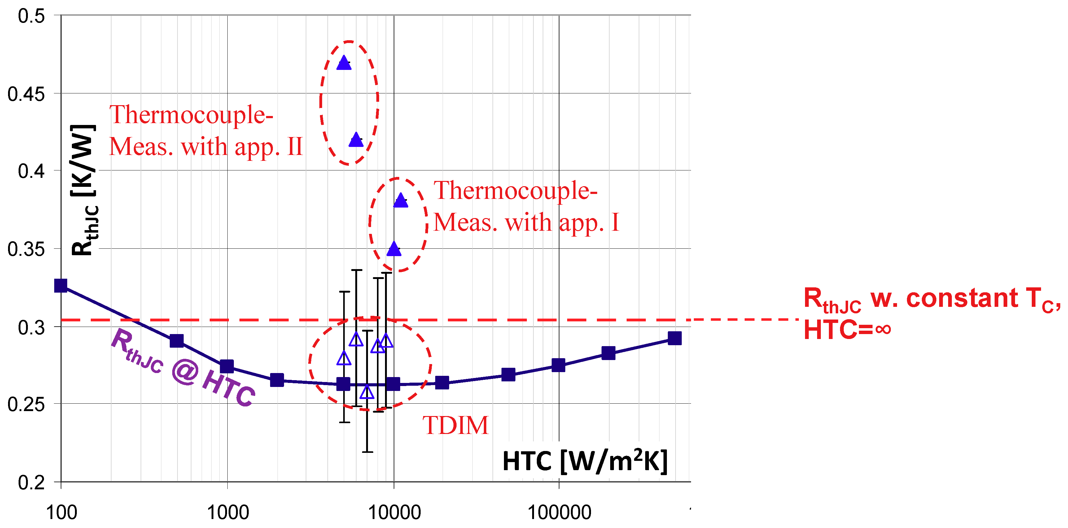
A deep analysis carried out at Infineon and presented in Reference [
22] compares:
Simulated RthJC values with an ideal heat sink, considered as a fixed-temperature case surface corresponding to an infinite heat transfer coefficient;
Simulated RthJC values in a wide range of heat transfer coefficients;
Measured values in two laboratories with two-point measurements;
TDIM measurements.
A realistic estimation of the heat transfer coefficient of a cold plate is approximately 3000–6000 W/m
2K. For this reason, in a first comparison we took the result of the “floating case” FE simulation around these heat transfer coefficients as the basis for evaluating the values obtained with other methodologies. In the second column of
Table 3, the measured
RthJC value is shown, and in the third and fourth columns, the Δ
RthJC1 difference from the simulated reference value in absolute numbers and percentage, respectively. The reference values are highlighted in
Table 3 with the bold border of the first row.
In an other approach we can compare the values from all methodologies to the two-point measurements (fifth column in the table, the fourth row highlighted with bold border as reference).
The RthJC values from finite element simulation with both heat sink models were systematically lower than the values obtained by thermocouple measurements in two different thermal labs using different setups (apparatus I and II). Thermocouple measurements were 34%–83% higher than those predicted by simulation with realistic heat sink (floating case temperature boundary condition). The TDIM measurements provided only slightly higher values than the reference.
It was identified that the root cause of the large scatter in the measured values was that it was hard to accurately measure the case temperature with a thermocouple, as the operator cannot guarantee that the thermocouple actually measures the true TC temperature of the package and not the temperature of the heat sink or some average value in between. Still, the repeatability of the measurements was surprisingly good at the same site, same equipment, and with operators having the same training.
On the other hand, the reproducibility of the values from thermocouple measurements at different laboratories was poor. Taking the higher value as reference from the site producing lower values systematically, we still experienced up to a 26% deviation as shown in the last column in
Table 3.
The repeatability of the TDIM measurements was good, because the measurement of the case temperature was not involved.
The accuracy of the TDIM technique is limited by other factors, for example, by noise in the
Zth measurement, the influence of the thermal interface on the separation point [
3], and the finite resolution of the structure function [
2]. The assessment of the accuracy is always difficult, since there are no exact reference values for
RthJC. Based on the experience of several hundred measurements and on comparisons with simulations, it is estimated that the accuracy of the TDIM method is approximately 15% (see error bars in
Figure 19). While this seems to be not overly accurate, it is still a lot better than the reproducibility of the two-point measurements shown in the table and chart above.
Laboratories having both kinds of instruments reported junction to case thermal resistances measured with the two-point method as 20% lower to 50% higher than the TDIM result [
22].
An elaborated study on the repeatability of junction to case thermal resistance values for larger packages with complex internal structures (i.e., FCBGA, CABGA) is presented in Reference [
26]. A sort of round robin testing was carried out with three operators using the two-point measurement concept. The series of tests was built up in a way that first all operators used the same piece of equipment and the same calibration data, then each operator recalibrated the devices under test, but they used the same equipment, then separate instruments of identical composition were used. The variation of measured data was below 8%. This variation quickly grew when the composition of the cold plate and the heat transfer coefficient of the measurement environment were changed. A similar study with associated simulation experiment is presented in Reference [
29].
The impact of run-in effects in the fixture used for the transient measurement is highlighted in Reference [
30].
A large round robin test involving several types of power LED devices was carried out in the European Delphi4LED project [
27]. It included the measurement of the optical and thermal parameters of the same LED samples at five different European research and academic institutions. They used the same make of test equipment but carried out the calibration and the thermal transient tests independently. The reproducibility of the measured thermal resistance values was surprisingly good, within 1%–2% [
27].
9. Discussion
Thermal testing has always been an integral part of the testing scheme of active components, but its importance has significantly grown with the advent of newer discrete devices and modules which are built of large and thin chips and package materials of high thermal conductivity.
Thermal tests are needed during all phases of development, and similar tests have to be carried out in the production again. Present trends extend thermal testing to the whole life cycle of an actual component including its live operation in the field. In the development phase, the performance of intermediate products can be revealed by thermal testing. At the end of the development data sheet values have to be provided for the ready product. However, single descriptive numbers like the RthJC junction to case thermal resistance cannot be used for adequate selection of a part for an actual design, as their definition is based on supposing isothermal surfaces which almost never exist in practice. Moreover, they are often based on measurements of poor reproducibility, and for this reason the values in data sheets are published with an unknown safety margin.
More complex compact thermal models composed of a net of thermal resistances can be better used in thermal characterization to enable the reliable design of equipment. These models reflect the behavior of the components in a more precise way without revealing confidential structural details. Such models can be derived from a set of thermal measurements and simulations.
In production, a larger number of tests have to be carried out. Related standards distinguish between type tests and routine tests.
Type tests are carried out on samples of new products in order to determine the electrical and thermal ratings of a type and for establishing test limits for further tests. Such tests are often of destructive nature. The type tests are repeated regularly on a given number of samples taken from manufacturing batches at the manufacturer or delivery batches at the end-user in order to confirm the quality of the product. Routine tests are carried out on each sample of the production or delivery.
The type tests repeated at regular production intervals and the routine tests have to be relatively simple and should not be time consuming. For this reason, so far, it seemed to be satisfactory to provide only simple numbers describing component quality derived from temperature measurements at dedicated accessible points of the component.
Other related test categories can be reliability tests and failure tests on faulty components. Measurement of thermal parameters for health monitoring in live operational systems is also gaining importance; such tests can be quasi-continuous or can be repeated time by time.
In all cases, the minimum time needed for carrying out a thermal test is significantly longer than the comparable time needed for electrical tests. For a discrete device several seconds are needed, and for a module, at least tens of seconds are needed to reach thermal stability. The steady state is reached through a heating transient which is followed by an inherent cooling transient, and the two are needed for an accurate thermal transient measurement.
All test types aim at determining the most critical thermal parameter, the semiconductor chip temperature from a transient event.
The best way to gain information on the chip temperature is selecting a temperature-dependent electric parameter of the active device, such as the forward voltage of an internal pn junction or the threshold voltage of a MOSFET, and mapping the value of this parameter to the approximate temperature of the chip. This voltage to temperature calibration process occurs in a thermostat; the parameter value is recorded at several temperatures. In order to ensure that the chip temperature does not significantly differ from the external temperature in this process, low power has to be maintained on the device during the calibration. A typical way is applying a low “measurement current” on a pn junction and recording the corresponding voltage.
But the actual thermal parameters can be determined only in a high-powered state. The only way to gain the semiconductor temperature at high power is by switching to the low measurement current used at calibration and checking the actual value of the calibrated temperature-sensitive parameter.
Present day transient test schemes switch down to measurement current once and record the cooling at a high sampling rate until the cold steady state is reached. This way accurate temperature data are collected for the whole cooling process, except for the short-time interval around the switching when the electric perturbation distorts the temperature signal.
Static test schemes switch down repetitively and use a not too sharply defined “proper time” for measuring the calibrated parameter at low power. Proper time is where the electric distortion already decays but the temperature of the chip still does not significantly drop. Static techniques may abort the cooling transient record after this time, but this is not explicitly stated in the related standards.
In both schemes, extrapolation techniques can be used for estimating the starting temperature just after switching.
Static and transient thermal tests can both be carried out by measuring the temperature at a single point in an assembly or at multiple accessible points.
In the case of a static test, the only way to obtain the thermal characteristics of a specific device or module within a larger assembly is by making temperature measurements at multiple accessible points, otherwise the segment in the heat conducting path belonging to the very device cannot be distinguished from the other parts of the assembly. In transient tests of a layered structure, portions of different thermal conductivity and specific heat can be mapped, and such partial thermal resistances can be determined, and even the internal temperature distribution can be concluded.
In the standardized transient dual interface measurement methodology (TDIM), in each thermal measurement, the whole heat conducting path is characterized, from the heat source to the ambient. This way distinguishing between component and test environment is achieved by the intentional structural change at the geometrical interface separating the device from the test bench (such as a cold plate).
We used simulation experiments and actual tests to analyze the accuracy, repeatability, and reproducibility of thermal tests. For demonstrating the concept, we selected the simplest thermal descriptors, the junction to case thermal resistance of a device and the junction to ambient thermal resistance of an assembly.
We verified with simulation experiments that the RthJC thermal metrics depend on the TIM quality used in the test bench, on the lateral displacement of the probe measuring the “case” temperature, on the penetration of the probe through the TIM, and on the heat transfer coefficient of the cold plate and other factors as well, resulting in a large uncertainty of the obtained value. In the case of a single-point transient test, the assembly is totally destroyed and rebuilt between the two measurements. Differences in TIM quality belong to the essence of the technique. Still, although the structure functions are highly reproducible, a decision on the threshold used has to be made in order to define at how large divergence it is considered to be the RthJC value.
In actual thermal tests we found that the accuracy, repeatability, and reproducibility of static and transient tests depend on the following:
Electrical transient at the switching process, as defined above;
Power measurement uncertainty on the device causes real ambiguities only at large modules with complex internal wiring;
Offset and gain errors in the data acquisition; these are the source of most reproducibility issues for multi-point measurements while indifferent in one-point transient measurements;
Reproducibility of the selected samples, such as die attach thickness, base plate roughness, and planarity;
Reproducibility of the test environment.
Regarding this last issue, different laboratories have different materials and geometries for the cold plate used in the measurements, other formations of the liquid flow, various surface roughness and planarity levels, and types and positions of external temperature sensors resulting in a large scatter of the obtained values.
We studied actual differences in static and transient measurements in several case studies. In the actual tests, we found that there was a systematic difference between the thermal data measured with the TDIM method and that measured with temperature probes, but this difference was smaller than the scatter in results measured at different laboratories with the latter method.


