Figure 1.
Basic structure of five-phase voltage source inverter (VSI).
Figure 1.
Basic structure of five-phase voltage source inverter (VSI).
Figure 2.
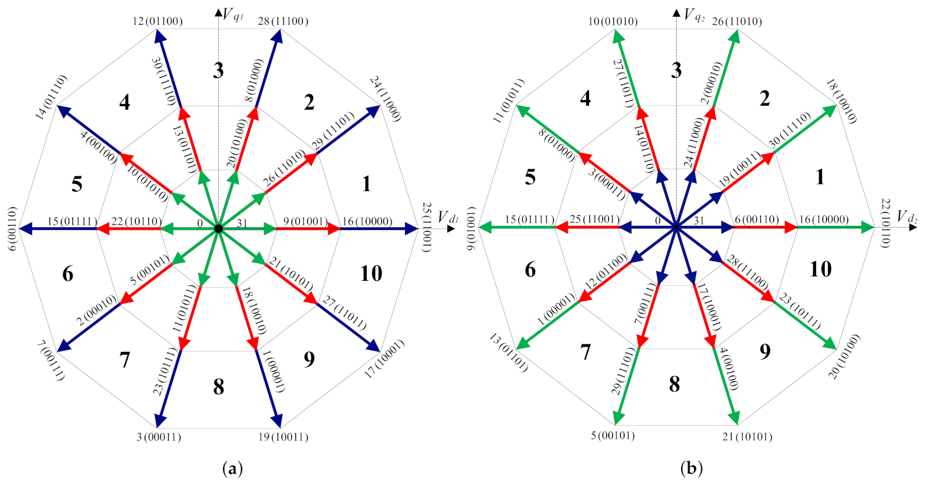
Two-dimension subspaces: (a) d1-q1 subspace, and (b) d2-q2 subspace.
Figure 2.
Two-dimension subspaces: (a) d1-q1 subspace, and (b) d2-q2 subspace.
Figure 3.
Vector ‘25’(11001) switching operation.
Figure 3.
Vector ‘25’(11001) switching operation.
Figure 4.
Five-phase inverter space vector modulation.
Figure 4.
Five-phase inverter space vector modulation.
Figure 5.
2L SVPWM modulation technique with a modulation index of 0.5: (a) Sector 1 applied vectors, (b) odd sector switching sequence, (c) filtered output voltage, and (d) voltage reference to the DC-Bus midpoint.
Figure 5.
2L SVPWM modulation technique with a modulation index of 0.5: (a) Sector 1 applied vectors, (b) odd sector switching sequence, (c) filtered output voltage, and (d) voltage reference to the DC-Bus midpoint.
Figure 6.
2L+2M SVPWM modulation technique with a modulation index of 0.5: (a) Sector 1 applied vectors, (b) odd sector switching sequence, (c) filtered output voltage, and (d) voltage reference to the DC-Bus midpoint.
Figure 6.
2L+2M SVPWM modulation technique with a modulation index of 0.5: (a) Sector 1 applied vectors, (b) odd sector switching sequence, (c) filtered output voltage, and (d) voltage reference to the DC-Bus midpoint.
Figure 7.
4L SVPWM modulation technique with a modulation index of 0.5: (a) Sector 1 applied vectors, (b) odd sector switching sequence, (c) filtered output voltage, and (d) voltage reference to the DC-Bus midpoint.
Figure 7.
4L SVPWM modulation technique with a modulation index of 0.5: (a) Sector 1 applied vectors, (b) odd sector switching sequence, (c) filtered output voltage, and (d) voltage reference to the DC-Bus midpoint.
Figure 8.
DPWM-MAX modulation techniques with modulation index of 0.5: (a) 2L-filtered output voltage, (b) 2L+2M-filtered output voltage, (c) 4L-filtered output voltage, (d) 2L voltage reference to the DC-Bus midpoint, (e) 2L+2M voltage reference to the DC-Bus midpoint, and (f) 4L voltage reference to the DC-Bus midpoint.
Figure 9.
DPWM-MIN modulation techniques with modulation index of 0.5: (a) 2L-filtered output voltage, (b) 2L+2M-filtered output voltage, (c) 4L-filtered output voltage, (d) 2L voltage reference to the DC-Bus midpoint, (e) 2L+2M voltage reference to the DC-Bus midpoint, and (f) 4L voltage reference to the DC-Bus midpoint.
Figure 10.
DPWM-V1 modulation techniques with modulation index of 0.5: (a) 2L-filtered output voltage, (b) 2L+2M-filtered output voltage, (c) 4L-filtered output voltage, (d) 2L voltage reference to the DC-Bus midpoint, (e) 2L+2M voltage reference to the DC-Bus midpoint, and (f) 4L voltage reference to the DC-Bus midpoint.
Figure 11.
Matlab/Simulink and PLECS simulation scheme.
Figure 11.
Matlab/Simulink and PLECS simulation scheme.
Figure 12.
Power loss look-up tables of C2M0160120D: (a) Turn-on losses; and (b) conduction losses.
Figure 12.
Power loss look-up tables of C2M0160120D: (a) Turn-on losses; and (b) conduction losses.
Figure 13.
Output voltage total harmonic distortion (THD) comparison.
Figure 13.
Output voltage total harmonic distortion (THD) comparison.
Figure 14.
Output voltage weighted total harmonic distortion (WTHD) comparison.
Figure 14.
Output voltage weighted total harmonic distortion (WTHD) comparison.
Figure 15.
CMV waveforms of the techniques: (a) 2L SVPWM, (b) 2L+2M SVPWM, (c) 4L SVPWM.
Figure 15.
CMV waveforms of the techniques: (a) 2L SVPWM, (b) 2L+2M SVPWM, (c) 4L SVPWM.
Figure 16.
CMV energy analysis comparison.
Figure 16.
CMV energy analysis comparison.
Figure 17.
Power losses: (a) conduction losses, and (b) switching losses.
Figure 17.
Power losses: (a) conduction losses, and (b) switching losses.
Figure 18.
Inverter efficiency.
Figure 18.
Inverter efficiency.
Figure 19.
Experimental setup.
Figure 19.
Experimental setup.
Figure 20.
Experimental efficiency at modulation index values of: (a) 0.9, (b) 0.7, (c) 0.5, and (d) 0.3.
Figure 20.
Experimental efficiency at modulation index values of: (a) 0.9, (b) 0.7, (c) 0.5, and (d) 0.3.
Table 1.
Vectors’ magnitudes on the d1-q1 subspace.
Table 1.
Vectors’ magnitudes on the d1-q1 subspace.
| Vector | Magnitude |
|---|
| Zero vector | 0 * |
| Small vector | 0.4944 * |
| Medium vector | 0.8 * |
| Large vector | 1.2944 * |
Table 2.
Reference summary of five-phase SVM techniques.
Table 2.
Reference summary of five-phase SVM techniques.
| SVM Technique | References |
|---|
| Two large vectors (2L SVPWM) | [26,46] |
| Two large and two medium vectors (2L+2M SVPWM) | [26,28,46,47] |
| Four large vectors (4L SVPWM) | [27,28] |
| Discontinuous SVM | [28] |
Table 3.
Switching sequence for 2L SVPWM discontinuous modulation techniques.
Table 3.
Switching sequence for 2L SVPWM discontinuous modulation techniques.
| Version | Odd Sector | Even Sector |
|---|
| 2L DPWM-MAX | VB, VA, V31, VA, VB | VA, VB, V31, VB, VA |
| 2L DPWM-MIN | V0, VB, VA, VB, V0 | V0, VA, VB, VA, V0 |
| 2L DPWM-V1 | V0, VB, VA, VB, V0 | VA, VB, V31, VB, VA |
| 2L DPWM-V2 | VB, VA, V31, VA, VB | V0, VA, VB, VA, V0 |
Table 4.
Switching sequence for 2L+2M SVPWM discontinuous modulation techniques.
Table 4.
Switching sequence for 2L+2M SVPWM discontinuous modulation techniques.
| Version | Odd Sector | Even Sector |
|---|
| 2L+2M DPWM-MAX | VAM, VBL, VAL, VBM, V31, VBM, VAL, VBL, VAM | VBM, VAL, VBL, VAM, V31, VAM, VBL, VAL, VBM |
| 2L+2M DPWM-MIN | V0, VAM, VBL, VAL, VBM, VAL, VBL, VAM, V0 | V0, VBM, VAL, VBL, VAM, VBL, VAL, VBM, V0 |
| 2L+2M DPWM-V1 | V0, VAM, VBL, VAL, VBM, VAL, VBL, VAM, V0 | VBM, VAL, VBL, VAM, V31, VAM, VBL, VAL, VBM |
| 2L+2M DPWM-V2 | VAM, VBL, VAL, VBM, V31, VBM, VAL, VBL, VAM | V0, VBM, VAL, VBL, VAM, VBL, VAL, VBM, V0 |
Table 5.
Switching sequence for 4L SVPWM discontinuous modulation techniques.
Table 5.
Switching sequence for 4L SVPWM discontinuous modulation techniques.
| Version | Odd Sector | Even Sector |
|---|
| 4L DPWM-MAX | VCL, VAL, VBL, VDL, V31, VDL, VBL, VAL, VCL | VDL, VBL, VAL, VCL, V31, VCL, VAL, VBL, VDL |
| 4L DPWM-MIN | V0, VCL, VAL, VBL, VDL, VBL, VAL, VCL, V0 | V0, VDL, VBL, VAL, VCL, VAL, VBL, VDL, V0 |
| 4L DPWM-V1 | V0, VCL, VAL, VBL, VDL, VBL, VAL, VCL, V0 | VDL, VBL, VAL, VCL, V31, VCL, VAL, VBL, VDL |
| 4L DPWM-V2 | VCL, VAL, VBL, VDL, V31, VDL, VBL, VAL, VCL | V0, VDL, VBL, VAL, VCL, VAL, VBL, VDL, V0 |
Table 6.
Simulation parameters.
Table 6.
Simulation parameters.
| Parameter | Value |
|---|
| Resistance, R | 34 |
| Inductance, L | 6 mH |
| DC-Bus | 550 V |
| Fundamental frequency | 50 Hz |
| Switching frequency | 50 kHz |
| External gate resistor, Rg(ext) | 6.5 |
| Junction temperature | 125 C |
Table 7.
C2M0160120D electrical characteristics.
Table 7.
C2M0160120D electrical characteristics.
| Parameter | Value |
|---|
| Breakdown voltage, Vblock | 1200 V |
| Drain current, I | 19 A |
| Gate-source voltage max | −10/+25 V |
| Gate-source voltage used | −5/+20 V |
| On-state resistance, RDS(on) | 290 m |
| Diode forward voltage | 3.1 V |
| Continuous diode forward current | 19 A |
Table 8.
Common-mode voltage (CMV) values of each vector on d1-q1.
Table 8.
Common-mode voltage (CMV) values of each vector on d1-q1.
| Vector | CMV Value |
|---|
| Zero vector | 0.5 * Vdc |
| Small vector | 0.1 * Vdc |
| Medium vector | 0.3 * Vdc |
| Large vector | 0.1 * Vdc |
Table 9.
Five-phase modulation techniques CMV dv/dt values and number of transitions in a switching period.
Table 9.
Five-phase modulation techniques CMV dv/dt values and number of transitions in a switching period.
| Modulation Technique | dv/dt Level | Number of Transitions | dv/dt Level | Number of Transitions |
|---|
| 2L SVPWM | 0.2 * Vdc/dt | 2 | 0.4 * Vdc/dt | 4 |
| 2L DPWM-MIN | 0.2 * Vdc/dt | 2 | 0.4 * Vdc/dt | 2 |
| 2L DPWM-MAX | 0.2 * Vdc/dt | 2 | 0.4 * Vdc/dt | 2 |
| 2L DPWM-V1 | 0.2 * Vdc/dt | 2 | 0.4 * Vdc/dt | 2 |
| 2L DPWM-V2 | 0.2 * Vdc/dt | 2 | 0.4 * Vdc/dt | 2 |
| 2L+2M SVPWM | 0.2 * Vdc/dt | 10 | 0.4 * Vdc/dt | – |
| 2L+2M DPWM-MIN | 0.2 * Vdc/dt | 8 | 0.4 * Vdc/dt | – |
| 2L+2M DPWM-MAX | 0.2 * Vdc/dt | 8 | 0.4 * Vdc/dt | – |
| 2L+2M DPWM-V1 | 0.2 * Vdc/dt | 8 | 0.4 * Vdc/dt | – |
| 2L+2M DPWM-V2 | 0.2 * Vdc/dt | 8 | 0.4 * Vdc/dt | – |
| 4L SVPWM | 0.2 * Vdc/dt | 6 | 0.4 * Vdc/dt | 4 |
| 4L DPWM-MIN | 0.2 * Vdc/dt | 6 | 0.4 * Vdc/dt | 2 |
| 4L DPWM-MAX | 0.2 * Vdc/dt | 6 | 0.4 * Vdc/dt | 2 |
| 4L DPWM-V1 | 0.2 * Vdc/dt | 6 | 0.4 * Vdc/dt | 2 |
| 4L DPWM-V2 | 0.2 * Vdc/dt | 6 | 0.4 * Vdc/dt | 2 |
Table 10.
Experimental THD.
Table 10.
Experimental THD.
| Modulation Technique | Modulation Index |
|---|
| 0.3 | 0.5 | 0.7 | 0.9 |
|---|
| 2L SVPWM | 29.20% | 29.16% | 29.29% | 29.21% |
| 2L DPWM-MIN | 29.40% | 29.14% | 29.16% | 29.05% |
| 2L DPWM-MAX | 29.11% | 29.00% | 29.04% | 29.04% |
| 2L DPWM-V1 | 29.00% | 29.04% | 28.97% | 28.99% |
| 2L DPWM-V2 | 29.17% | 29.04% | 28.96% | 28.96% |
| 2L+2M SVPWM | 3.02% | 2.45% | 2.16% | 1.36% |
| 2L+2M DPWM-MIN | 4.72% | 3.25% | 2.87% | 2.27% |
| 2L+2M DPWM-MAX | 4.41% | 3.39% | 3.00% | 2.79% |
| 2L+2M DPWM-V1 | 4.63% | 3.55% | 3.25% | 2.77% |
| 2L+2M DPWM-V2 | 4.89% | 3.95% | 3.44% | 2.84% |
| 4L SVPWM | 3.03% | 2.53% | 2.21% | 1.41% |
| 4L DPWM-MIN | 4.03% | 3.76% | 3.23% | 2.35% |
| 4L DPWM-MAX | 3.80% | 3.46% | 3.07% | 2.89% |
| 4L DPWM-V1 | 3.95% | 3.68% | 3.26% | 2.96% |
| 4L DPWM-V2 | 4.14% | 3.72% | 3.13% | 3.02% |
Table 11.
Experimental WTHD.
Table 11.
Experimental WTHD.
| Modulation Technique | Modulation Index |
|---|
| 0.3 | 0.5 | 0.7 | 0.9 |
|---|
| 2L SVPWM | 9.62% | 9.58% | 9.65% | 9.62% |
| 2L DPWM-MIN | 9.69% | 9.61% | 9.61% | 9.57% |
| 2L DPWM-MAX | 9.59% | 9.56% | 9.57% | 9.57% |
| 2L DPWM-V1 | 9.51% | 9.55% | 9.55% | 9.55% |
| 2L DPWM-V2 | 9.59% | 9.56% | 9.54% | 9.54% |
| 2L+2M SVPWM | 0.44% | 0.44% | 0.47% | 0.38% |
| 2L+2M DPWM-MIN | 0.98% | 0.60% | 0.63% | 0.61% |
| 2L+2M DPWM-MAX | 0.95% | 0.84% | 0.78% | 0.73% |
| 2L+2M DPWM-V1 | 0.68% | 0.63% | 0.59% | 0.53% |
| 2L+2M DPWM-V2 | 0.76% | 0.64% | 0.64% | 0.52% |
| 4L SVPWM | 0.49% | 0.47% | 0.49% | 0.43% |
| 4L DPWM-MIN | 0.88% | 0.83% | 0.77% | 0.79% |
| 4L DPWM-MAX | 0.87% | 0.85% | 0.74% | 0.69% |
| 4L DPWM-V1 | 0.72% | 0.79% | 0.70% | 0.66% |
| 4L DPWM-V2 | 0.79% | 0.80% | 0.73% | 0.67% |
Table 12.
Experimental CMV normalized energy.
Table 12.
Experimental CMV normalized energy.
| Modulation Technique | Modulation Index |
|---|
| 0.3 | 0.5 | 0.7 | 0.9 |
|---|
| 2L SVPWM | 1.76 | 1.43 | 1.01 | 0.59 |
| 2L DPWM-MIN | 0.49 | 0.64 | 0.57 | 0.56 |
| 2L DPWM-MAX | 0.50 | 0.64 | 0.57 | 0.55 |
| 2L DPWM-V1 | 1.61 | 1.37 | 0.98 | 0.68 |
| 2L DPWM-V2 | 1.61 | 1.37 | 0.99 | 0.68 |
| 2L+2M SVPWM | 1.75 | 1.45 | 1.07 | 0.68 |
| 2L+2M DPWM-MIN | 0.69 | 0.90 | 0.79 | 0.63 |
| 2L+2M DPWM-MAX | 0.70 | 0.90 | 0.80 | 0.63 |
| 2L+2M DPWM-V1 | 1.60 | 1.45 | 1.03 | 0.67 |
| 2L+2M DPWM-V2 | 1.60 | 1.46 | 1.03 | 0.67 |
| 4L SVPWM | 1.62 | 1.14 | 0.60 | 0.38 |
| 4L DPWM-MIN | 0.54 | 0.63 | 0.47 | 0.34 |
| 4L DPWM-MAX | 0.54 | 0.62 | 0.46 | 0.34 |
| 4L DPWM-V1 | 1.54 | 1.12 | 0.78 | 0.33 |
| 4L DPWM-V2 | 1.53 | 1.12 | 0.78 | 0.33 |
Table 13.
Performance comparison between each modulation.
Table 13.
Performance comparison between each modulation.
| General Features | Efficiency | Efficiency | Switching | Conduction | CMV | CMV | CMV Freq. | CMV Freq. | Voltage |
|---|
| | mi ≤ 0.5 | mi > 0.5 | Losses | Losses | Max. Level | Transitions | Comps Energy | Comps Energy | THD |
|---|
| | | | | | | | mi ≤ 0.6 | mi > 0.6 | |
|---|
| 2L SVPWM | Low | High | High | Moderate | 0.4 * Vdc | 6 | High | Moderate | High |
| 2L DPWM-MIN | Medium | High | Moderate | Moderate | 0.4 * Vdc | 4 | Low | Moderate | High |
| 2L DPWM-MAX | Medium | High | Moderate | Moderate | 0.4 * Vdc | 4 | Low | Moderate | High |
| 2L DPWM-V1 | High | High | Low | Moderate | 0.4 * Vdc | 4 | High | Moderate | High |
| 2L DPWM-V2 | High | High | Low | Moderate | 0.4 * Vdc | 4 | High | Moderate | High |
| 2L+2M SVPWM | Low | High | High | Moderate | 0.2 * Vdc | 10 | High | Moderate | Low |
| 2L+2M DPWM-MIN | Medium | High | Moderate | Moderate | 0.2 * Vdc | 8 | Low | Moderate | Low |
| 2L+2M DPWM-MAX | Medium | High | Moderate | Moderate | 0.2 * Vdc | 8 | Low | Moderate | Low |
| 2L+2M DPWM-V1 | Medium | High | Moderate | Moderate | 0.2 * Vdc | 8 | High | Moderate | Low |
| 2L+2M DPWM-V2 | Medium | High | Moderate | Moderate | 0.2 * Vdc | 8 | High | Moderate | Low |
| 4L SVPWM | Low | High | High | Moderate | 0.4 * Vdc | 10 | High | Low | Low |
| 4L DPWM-MIN | Medium | High | Moderate | Moderate | 0.4 * Vdc | 8 | Low | Low | Low |
| 4L DPWM-MAX | Medium | High | Moderate | Moderate | 0.4 * Vdc | 8 | Low | Low | Low |
| 4L DPWM-V1 | Medium | High | Moderate | Moderate | 0.4 * Vdc | 8 | High | Low | Low |
| 4L DPWM-V2 | Medium | High | Moderate | Moderate | 0.4 * Vdc | 8 | High | Low | Low |


