Abstract
The power conversion efficiency of lead halide perovskite solar cells has been elevated to 25.2%. However, the toxicity of lead and the complex fabrication process of those cells considerably hinder the commercial application of such solar cells. Therefore, lead-free solar cells with comparable power conversion efficiency with a much lower environmental impact have recently attracted enormous attention in both academia and industry. This paper presents a theoretical study to assess the energy conversion capacity of lead-free perovskite solar cells with MASnI3 perovskite as its absorber layer using solar cell capacitance simulator (SCAPS). In particular, the effects of materials of the perovskite solar cells’ electron transport layers (ETLs) and hole transport layers (HTLs) on their energy conversion performance are elaborated. Our results show that Cd0.5Zn0.5S and MASnBr3 are the most suitable materials for ETL and HTL, respectively. It is also found from that the solar cell performance can be further enhanced through optimizing the thickness and defect density of its absorber layer. Moreover, the effects of defect densities in interface layers are investigated. In addition, the effects of ETL and HTL doping densities as well as influences of the back-contact work function and operating temperature of the tin-based perovskite solar cells are discussed. Finally, a glass substrate/FTO/Cd0.5Zn0.5S (ETL)/MASnI3/MASnBr3 (HTL)/back-contact solar cell with a power conversion efficiency of 23.86% is recommended for further optimization.
1. Introduction
Perovskites are considered as promising candidate materials for photovoltaic solar energy conversion because of their outstanding photovoltaic properties such as long electron–hole diffusion length, large optical absorption coefficient, small carrier effective mass, low processing temperature, and strong excitonic transition. Among different types of perovskite solar cells (PSCs), the organic–inorganic metal halide PSCs have received significant attention years because they have high power conversion efficiency (PCE) can be fabricated straightforwardly at relatively low cost [1,2].
Methyl ammonium lead tri-iodide (MAPbI3) has long been considered as a perovskite material and extensively used for PSCs. However, commercial application of the MAPbI3-based PSCs is considerably hindered because the lead in MAPbI3 is very toxic [3,4,5], which leads to an appreciation of lead-free PSCs in the field of photovoltaic technology. Normally, a PSC should include an electron transport layer (ETL) and a hole transport layer (HTL) to maximize its power conversion efficiency by extracting and transporting photogenerated electrons, modifying the interface, aligning the interfacial energy level, and minimizing the charge recombination in PSC (for ETL [6]), as well as improving hole extraction and selectively blocking electrons to diminish electron–hole recombination on anode (for HTL [7]). The most commonly used materials for ETL and HTL are titanium dioxide (TiO2) and Spiro-OMeTAD, respectively. However, the high-temperature deposition of TiO2 and the high price of Spiro-OMeTAD remain as noticeable barriers that prevent practical applications of those materials in commercializable PSCs. Moreover, Spiro-OMeTAD is an unstable material, which can deteriorate the performance of the PSCs. Therefore, seeking new ETL and HTL materials for the PSCs is crucial for broad application of such devices. Recent studies have proven that inorganic materials are more stable and offer higher carrier mobility than organic materials [8,9,10]. Hence, the application of inorganic charge-transport materials for the PSCs is highly desired.
Inorganic halide perovskites, such as Sn-, Ag-, Sb-, Bi-, Cu-, and Ge-based solar cells, have been investigated as possible replacements of lead [11,12,13]. Due to its optimal bandgap of 1.3 eV, a metal halide perovskite, CH3NH3SnI3, has been considered as a promising alternative for the lead-free PSCs [14]. Other environment-friendly lead-free perovskites, such as Cs2TiBr6 [15], Cs2TiBr6, Cs2TiI6, Cs2TiF6, and Cs2TiCl6 [16], have also been employed to develop lead-free PSCs by other researchers for the purpose of acquiring optimal solar cell performance. In addition to the perovskites, to achieve desired cell performance, an inorganic charge transport material, Zinc Tin Oxide (ZTO), was used as ETL in the PSCs because of its high charge carrier mobility. PSCs with ZTO as the prime ETL could reach 24.07% PCE with an open circuit voltage (Voc) of 1.13 eV, a short-circuit current density (Jsc) of 23.18 mA/cm2 and a fill factor (FF) of 67.66% [17]. A certain amount of Zn is added to the solution containing Cd and S ions to control the bandgap of the cadmium sulfide (CdS) ETL layer for higher cell performance. As found by Baig et al. [14], the bandgap of the Cd1-xZnxS layer heavily depended on the concentration of Zn. Other ETL materials, such as indium gallium zinc oxide (IGZO), Tin (IV) oxide (SnO2), C60, TiO2, zinc oxide (ZnO), and phenyl-C61-butyric acid methyl ester (PCBM), were also tested by Lakhdar and Hima [18] to evaluate their effects in improving the cell performance. In terms of HTL, inorganic p-type materials including ZnO, copper (I) thiocyanate (CuSCN), copper (I) oxide (Cu2O), P3HT, copper (I) iodide (CuI), and nickel (II) oxide (NiO) have been used as the HTL materials because of their low cost and high performance-degradation resistance [19,20]. For instance, a recent study found that the PSCs with (ZnO) as their HTLs could reach 25.02% PCE [19].
In this study, the performance of the lead-free PSCs with the same configuration, glass/FTO/ETL/IL1/MASnI3/IL2/HTL/Au (Figure 1), and different ETL and HTL materials are determined and compared. As shown in Figure 1, the proposed lead-free PSCs include a glass substrate, a front electrode layer made of FTO, an ETL made of candidate materials, a MASnI3 perovskite absorber layer, an HTL made of candidate layers, and a back electrode layer made of gold. IL1 and IL2 are the ETL/perovskite interface layer and the perovskite/HTL interface layer, respectively. Candidate ETL materials include carbon 60 (C60), CdS, Cd0.5Zn0.5S, IGZO, PCBM, ZnO, and TiO2, while the candidate HTL materials are Cu2O, CuI, CuSCN, MASnBr3, NiO, poly polystyrene sulfonate (PEDOT:PSS), and Spiro-OMeTAD. In addition, the thickness and defect density of the absorber layer (the MASnI3 layer) are further optimized. Moreover, the effects of interface layers defect densities are discussed, and the effects of ETL and HTL doping densities as well as the influence of back-contact work function and operating temperature on the cell performance are demonstrated.
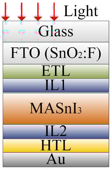
Figure 1.
Configuration of the lead-free PSC.
2. Materials and Methodology
2.1. Device Structure and Input Parameters
Figure 1 illustrates the structure of a benchmark PSC device first simulated in the present study. In that structure, MASnI3 is utilized as the perovskite absorption layer, fluorine-doped tin oxide (FTO or SnO2:F) is chosen as the transparent conducting oxide, and gold (Au) is selected for the back contact. Common materials TiO2 and Spiro-OMeTAD are initially used as the ETL and HTL, respectively. However, different ETL and HTL materials are tested later to find the best materials that maximize the cell performance. Key simulation parameters for those layers are obtained from previous experimental and theoretical analyses [14,19,21,22] and are summarized in Table 1. Two interface layers are inserted between the ETL and the MASnI3 perovskite layer (ETL/perovskite interface) and the perovskite layer and HTL (perovskite/HTL interface), respectively. Those interface layers are added because the interfaces play a critical role in capturing electrons and holes. The defects in the perovskite layer are set to be in the neutral Gaussian distribution, with characteristic energy of 0.1 eV and energy above the valence band of 0.6 eV [23]. In contrast, the defects in the ETL/perovskite and perovskite/HTL interfaces are considered to be neutral single defects (as set in SCAPS [23]), with an energy of 0.6 eV above the valence band. The simulation is carried out using solar cell capacitance simulator (SCAPS) software under AM1.5G solar illumination with an incident power density of 100 mW/cm2 and the input parameters listed in Table 1. The simulation results are obtained as Voc = 0.84 V, Jsc = 29.64 mA/cm2, FF = 69.27%, and PCE = 17.24%. More details about the numerical method embedded in SCAPS are elaborated in Section 2.2.

Table 1.
Input parameters for simulation of PSC performance.
To find the best ETL and HTL materials, more simulations are conducted following the same approach with a variety of materials for ETL (C60, CdS, Cd0.5Zn0.5S, IGZO, PCBM, and ZnO) and HTL (Cu2O, CuI, CuSCN, MASnBr3, NiO, and PEDOT:PSS). To compare the performance of the PSCs with different ETL and HTL materials with the performance of the PSC with the TiO2 ETL and Spiro-OMeTAD HTL, the thicknesses of all the ETLs and HTLs are maintained at 100 and 200 nm, respectively. Simulation parameters for different ETL and HTL materials are obtained from published articles (see [14,18,19,24,25] (for ETL materials) and [14,19,21,25] (for HTL materials)), as listed in Table 2 and Table 3, respectively.
Table 2.
Input parameters for different ETL materials.
Table 3.
Input parameters for different HTL materials.
The solubility of MASnI3 is different from the solubility of carrier transporting layers proposed in this paper. Generally, the ETL is not affected much by the perovskite layer. The perovskite layer is relatively stable after annealing and the HTL spin coating process is fast, so the HTL has little effect on the perovskite layer. The ETL materials (C60 [26], CdS [27], Cd0.5Zn0.5S [14], IGZO [18,19], ZnO [28], and PCBM [18,29]) and HTL materials (Cu2O [29], CuI [30,31], CuSCN [32,33], MASnBr3 [14], NiO [34], and PEDOT:PSS [26]) proposed in this paper are feasible and have been verified in the reported articles.
2.2. Numerical Method
Numerical simulations involved in this study are carried out using SCAPS software, an efficient one-dimensional solar cell simulation program developed by researchers at the University of Ghent [24]. Using that software, the spectral response of solar energy, J-V characteristics, and electric field distribution can be obtained by solving the Poisson equation (Equation (1)) and the continuity equation for electrons (Equation (2)) and holes (Equation (3)) that are embedded in SCAPS.
where ε is the relative permittivity; Na and Nd are the ionized acceptor concentration and ionized donor concentration, respectively; ψ is the electrostatic potential; x indicates the coordinate position; p and n represent the number of holes and electrons, respectively; pt and nt represent the number of trapped holes and electrons; Jp and Jn denote the current density of holes and electrons; Rp(x) and Rn(x) are the recombination rate of holes and electrons; and G(x) denotes the optical generation rate.
3. Results and Discussion
3.1. Effects of ETL Materials on Cell Performance
The simulation results obtained for the PSCs with the proposed ETL materials listed in Table 2 and the benchmark Spiro-OMeTAD HTL are summarized in Table 4 and the obtained J-V characteristics are plotted in Figure 2. In Table 4, it can be found that the PSC with the C60 ETL yields the lowest PCE while the PSC with the Cd0.5Zn0.5S ETL acquires the highest PCE. The performances of the PSCs with the TiO2 ETL (the benchmark material) and ZnO are also acceptable.
Table 4.
Responses of PSCs with different ETL materials.
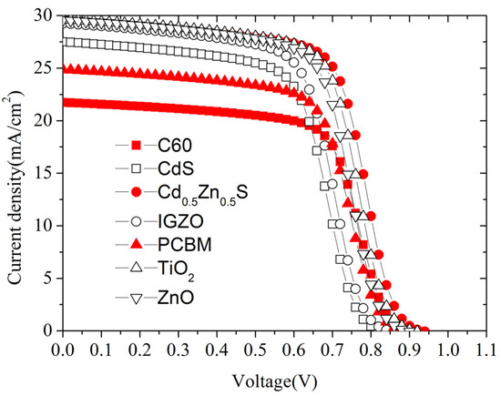
Figure 2.
Effect of different ETL materials on J-V characteristics.
Figure 3 shows the influence of different ETL materials on quantum efficiency (QE) of the PSCs. The figure shows that, when the incident wavelength is greater than 750 nm, the QE values calculated from different PSCs are almost the same. However, if the incident wavelength is less than 750 nm, the QE value yielded from the C60 ETL is the lowest among all calculated QE results, thereby leading to an inadequate photon absorption. In addition, the lowest electron mobility of C60 also restrains charge collection. Therefore, according to our simulation, C60 leads to the lowest JSC and PCE compared with other ETL materials and should not be selected for designing the lead-free PSCs.
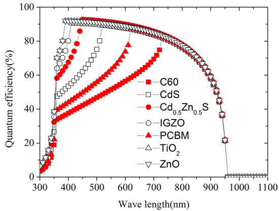
Figure 3.
Effect of different ETL materials on QE.
Figure 4 shows that the conduction band (CB) level of almost all tested ETL materials is higher than that of the MASnI3 perovskite, except for CdS. Conduction band offset (CBO) is defined as the difference between CB level of ETL and that of the perovskite. If the CB level of ETL is lower than that of the perovskite, CBO is negative, and an energy cliff will be formed at the ETL/perovskite interface. Otherwise, CBO is positive, and an energy spike will be formed. Therefore, an energy cliff is formed at the CdS/perovskite interface while energy spikes are generated at the interfaces between other ETL materials and the perovskite. The energy cliff does not hamper photo-generated electron flow. However, the activation energy for carrier recombination (the difference between the bandgap of perovskite and the absolute value of CBO) becomes lower than the bandgap of perovskite [35,36], which may cause the interface recombination to occupy the main position for recombination of the PSC device. Voc decreases as the recombination rate increases. Therefore, the PCE drops when Voc decreases and the PCE of the PSC with the CdS ETL is relatively low. For other ETL materials, the energy spike formed at the ETL/perovskite interface acts as a barrier for the photo-generated electrons, but the activation energy for carrier recombination is equal to the bandgap of the perovskite, so the activation energy is more than that calculated by energy cliff, which can certainly enhance the cell performance. It is also proved that energy spike within a small range has less effect on the motion of photo-generated electrons but greater impact on the carrier recombination rate [37]. The PSC with a Cd0.5Zn0.5S ETL yields a higher PCE because the CB level of Cd0.5Zn0.5S is higher than that of other ETL materials and its mobility is higher. However, as the CBO continues to increase, the performance will decrease due to the double-diode behavior [37]. Thus, Cd0.5Zn0.5S is finally selected as the optimal ETL material for the proposed lead-free PSC.
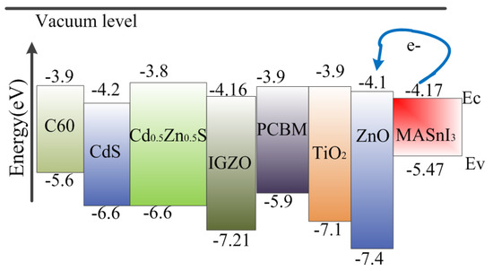
Figure 4.
Band alignment between ETL materials and MASnI3 perovskite.
3.2. Effects of HTL Materials on Cell Performance
After selecting the ETL, lead-free PSCs with the Cd0.5Zn0.5S ETL and different HTL materials as listed in Table 3 are simulated using SCAPS, and their predicted responses are listed in Table 5 and plotted in Figure 5, Figure 6 and Figure 7. As shown in Figure 5 and Figure 6, the J-V characteristics and the QE values of the PSCs with different HTL materials do not show significant difference. Table 5 shows that the PSC with the MASnBr3 HTL yields the highest PCE. Since the valence band (VB) level of MASnBr3 is lower than that of the MASnI3 perovskite (Figure 7), energy spike is formed at the perovskite/MASnBr3 interface, and the activation energy for carrier recombination is high, which leads to the high PCE. For the other HTL materials, since their VB levels are higher than that of MASnI3, energy cliffs will be formed at the perovskite/HTL interface. Similar to the case of the ETL materials, the energy cliffs do not impede the transportation of the photo-generated holes. However, due to the cliffs, the activation energy for carrier recombination becomes lower than the bandgap of the perovskite, which in turn increases the interface recombination and causes a reduction in the cell performance.
Table 5.
Responses of PSCs with different HTL materials.
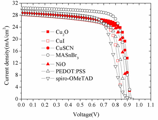
Figure 5.
Effect of different HTL materials on J-V characteristics.
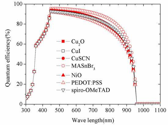
Figure 6.
Effect of different HTL materials on QE.
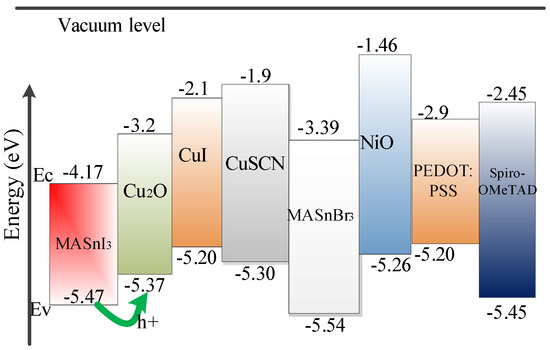
Figure 7.
Band alignment between HTL materials and MASnI3 perovskite.
When an energy cliff is formed, the activation energy for carrier recombination (Ea) is defined by
where Eg,absorber is the bandgap of the perovskite and Ev,absorber and Ev,HTL represent the VB levels of the perovskite and HTL, respectively. The values of Ea calculated for Cu2O, CuSCN, NiO, and CuI are 1.2, 1.13, 1.09, and 1.03 eV, respectively. The PCE values calculated from the PSCs with those HTL materials are ordered as: CuI < NiO < CuSCN < Cu2O. Obviously, there is a positive correlation between the Ea and PCE results. However, the PCE of the PSC with the Spiro-OMeTAD HTL is lower than those of the PSCs with other HTL materials despite the higher Ea (1.28 eV). This is because of the very low hole mobility of Spiro-OMeTAD. In summary, MASnBr3 is selected as the HTL material because it leads to the highest PCE. Thus, the optimized PSC with a Cd0.5Zn0.5S ETL and MASnBr3 HTL is used for the following simulations to find how other key parameters affect its performance.
3.3. Effect of Absorber Layer Thickness
The active perovskite absorber layer has a considerable influence on the cell performance. The effect of perovskite layer thickness on the cell performance is also inspected through numerical simulations, in which the thickness is assumed to vary from 100 to 10,000 nm. The simulation results are plotted in Figure 8. The figure shows that, as the absorber layer thickness increases, the Voc, Jsc, and PCE values rise while the FF keeps decreasing. The Jsc value increases because, as the absorber layer thickness increases, more photons will be absorbed by the layer. As a result, the elevation of the excess carrier concentration causes the Jsc to increase. On the other hand, as the absorber layer thickness increases, series resistance value in the solar cell and the internal power depletion would increase as well, leading to a continuous drop in FF. As depicted in Figure 8, when the thickness reaches and exceeds 500 nm, all those results become saturated.
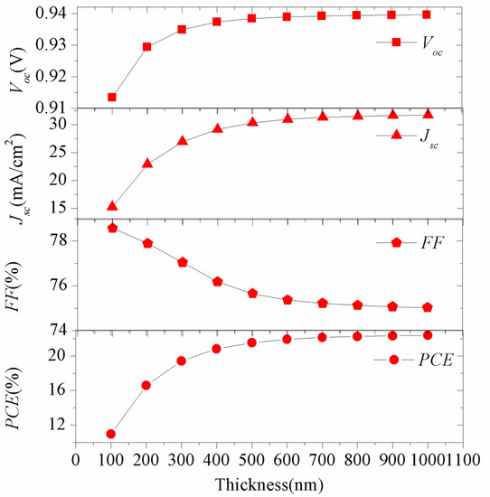
Figure 8.
Effect of absorber layer thickness on solar cell performance.
Voc can be calculated by
where n is a factor, nkT/q is the thermal voltage, IL represents the light generated current, and I0 is the dark saturation current. When the absorber layer gets thinner, the recombination of electrons and holes becomes weaker, causing I0 to decrease. On the other side, the concentration of excess carriers becomes higher as the increasing of thickness, causing IL to increase and therefore leading to an enhanced Voc (Equation (5)) [38].
PCE can be jointly determined by Voc, JSC, and FF as
where Ps is the irradiance from the Sun to the Earth. It can be readily deduced that PCE increases as the thickness increases by extracting Jsc, Voc, and FF values from the results in Figure 8 and substituting them into Equation (6).
3.4. Effect of Absorber Layer Defect Density
Photo-generated electrons are primarily generated in the perovskite absorber layer. Hence, the cell performance is significantly determined by the properties of perovskite absorption films. Defect density is an important indicator of the quality of the absorption films. A perovskite absorber layer with a higher defect density has lower quality and its carrier recombination rate is stronger than its carrier generation rate [39]. In this paper, the performances of PSCs with different absorption layer defect densities are simulated to determine the influence of the layer defect density on the cell performance. Defect density values involved in this study range from 1013 to 1018 cm−3. As illustrated in Figure 9, when the defect density is below 1015 cm−3, the J-V characteristics of the PSC almost remain unchanged. The J-V characteristics start to deteriorate when the defect density continues to increase.
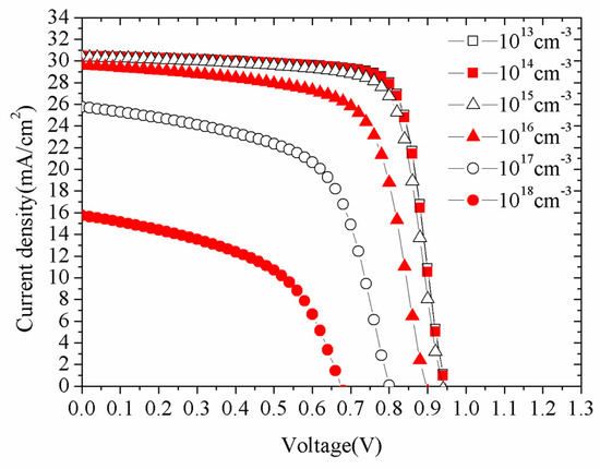
Figure 9.
Effect of absorber layer defect density on J-V characteristics.
A deep energy level defect acts as Shockley–Read–Hall nonradiative recombination center. Hence, as the defect density in the absorber layer increases, the short minority carrier lifetime will decrease while the charge recombination will increase, leading to a drop in Voc and Jsc. Furthermore, when the doping density is comparable to or lower than the defect density in the absorber, the PSC becomes semi-insulating and a desired p-n junction will not be formed [40], resulting in an inferior cell performance. Thus, to achieve an ideal PSC performance, the defect density in the absorber layer has to be minimized or even eliminated. However, it is still very difficult to significantly reduce the defect density with the present manufacturing advances. According to our results, to achieve a desired cell performance, the defect density in the absorber layer should be less than 1015 cm−3.
3.5. Effect of Interface Layer Defect Density
The properties of the interface layers have a critical impact on solar cell performance. A higher defect density decreases the layer quality and increases the recombination rate [40]. To discuss the effect of the interface layer defect density on the PSC performance, we assume that the defect densities of IL1 and IL2 vary from 1011 to 1021 cm−3.
Figure 10 and Figure 11 show the J-V characteristics of PSCs with different defect densities in IL1 and IL2, respectively. Figure 12 shows the effect of interface layer defect density on PCE. These figures show that a lower defect density in the interface layer will enhance Voc and Jsc, thereby promoting the PCE. Obviously, when the defect density of IL1 is below 1015 cm−3 and the defect density of IL2 is below 1017 cm−3, the effect of the defect density on the J-V characteristics becomes weak. However, if the interface layer defect density continues to increase, the PSC performance will deteriorate because higher defect densities in IL1 and IL2 will lead to more traps and recombination centers [38].
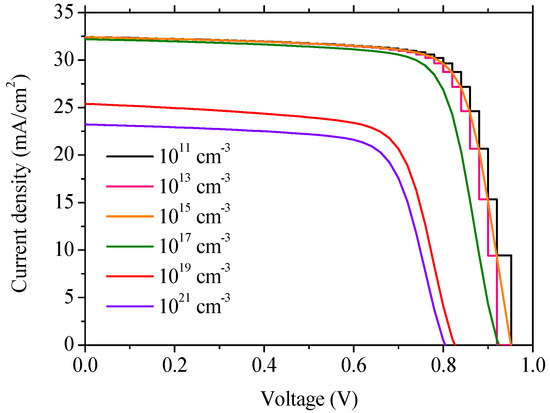
Figure 10.
Effect of IL1 defect density on J-V characteristics.
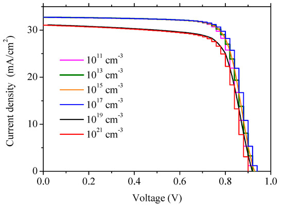
Figure 11.
Effect of IL2 defect density on J-V characteristics.
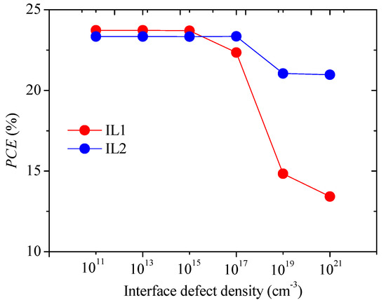
Figure 12.
Effect of interface defect density on PCE.
Compared with IL2, it is evident that the defect density of IL1 has a stronger influence on the PCE. This is because the number of electron–hole pairs generated at IL1 are much larger than IL2, and the higher excess carrier density will result in a higher recombination rate. According to our simulation results, the defect densities of IL1 and IL2 should be less than 1015 and 1017 cm−3, respectively, to achieve desired PSC performance.
3.6. Effect of Doping Density in ETL and HTL
The effects of the doping density in ETL and HTL on the PCE of PSC are displayed in Figure 13 and Figure 14, respectively. The curves in those figures show a similar trend, which is that the PCE rises gradually with the increasing of the doping density. This is because the increase in ETL donor doping concentration will lead to an improvement in conductivity of the ETL and a decrease in the reverse saturation current, both of which in turn leading to the growth of the PCE. An increase in HTL acceptor doping concentration will reduce resistivity of the HTL and therefore will enhance the current in the solar cell, which will cause the PCE to increase [25].
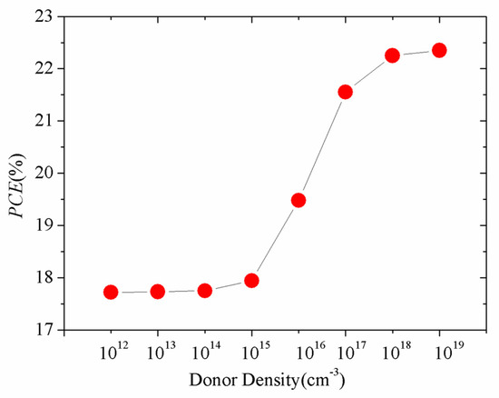
Figure 13.
Effect of ETL donor doping density on PCE.
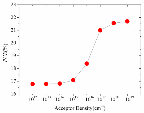
Figure 14.
Effect of HTL acceptor doping density on PCE.
Taking N-type doping as an example, the conductivity (σ) can be determined as σ = nqμn, where n is the electron concentration, μn is the electron mobility, and q is the electric charge. In the case of light doping, we have n ≈ Nd, where Nd is the ionized donor concentration. Then, we obtain σ ≈ Ndqμn. The mobility does not change much with Nd in the case of light doping, so there is a positive correlation between σ and Nd. This is similar for the P-type doping.
It can also be observed in these figures that the PCE grows slowly when the doping density exceeds 1017 cm−3. This is because, if the doping density continues to increase to a certain extent, high doping effects will appear due to the Moss–Burstein effect [41], which will impede the PSC performance.
3.7. Effect of Back-Contact Work Function
Figure 15 depicts the PCE results calculated from different back-contact work functions, which range from 4.6 to 5.1 eV. The figure shows that, when the back-contact work function decreases, the built-in voltage in solar cell decays, resulting a drop in Voc and an inefficient collection of photo-generated carriers, which therefore causes the Jsc to decrease. When the back-contact work function is below 4.9 eV, the cell performance deteriorates steeply due to the formation of a Schottky junction [24] at the MASnBr3/back-contact interface. The Schottky junction leads to S-shaped J-V characteristics and is a barrier for the hole movements. The Schottky barrier increases as the back-contact work function decreases, which impedes the hole transportation and causes the FF to decrease and PCE to deteriorate.
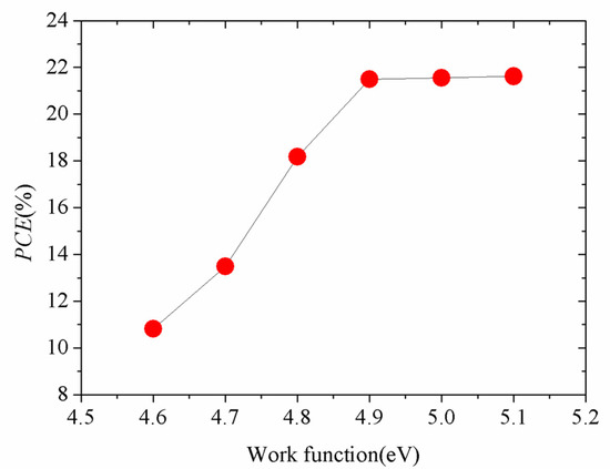
Figure 15.
Effect of back-contact work function on PCE.
3.8. Effect of Operating Temperature
In general, the operating temperature of solar cells is higher than 300 K. Therefore, in our simulation, the domain of the operating temperature is set from 300 to 500 K to study how the operating temperature influences the cell performance. Figure 16 plots the J-V characteristics of the PSC. As exhibited in that figure, the PSC performance deteriorates as the operating temperature increases. This might be because the increase of operating temperature will cause a decrease in Voc (Equation (7)), and consequently will hurt the PSC performance.
where T is the operating temperature and Eg and q are the bandgap and electric charge, respectively.
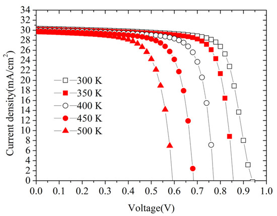
Figure 16.
Effect of operating temperature.
As shown in Equation (7), when the operating temperature increases, Voc drops, the reverse saturation current increases, and the PCE decreases. As declared by Devi et al. [40], electron and hole mobility, carrier concentration, and bandgap will change at high temperatures; therefore, the ambient temperature has a critical impact on the cell performance, as also confirmed by our simulation results.
Based on the simulation results, Cd0.5Zn0.5S and MASnBr3 are chosen for the ETL and HTL materials, respectively. It is also found that the PSC will achieve optimal performance when the absorber layer thickness is 500 nm; the defect density is maintained below 1015 cm−3; the defect densities of IL1 and IL2 are 1015 and 1017 cm−3, respectively; the ETL and HTL doping densities are 1017 cm−3; and the back-contact work function is 5.1 eV. Figure 17 compares the J-V characteristics before and after the optimization. The optimal PSC performance is indicated with Voc = 0.96 V, Jsc = 32.48 mA/cm2, FF = 76.40%, and PCE = 23.86%.
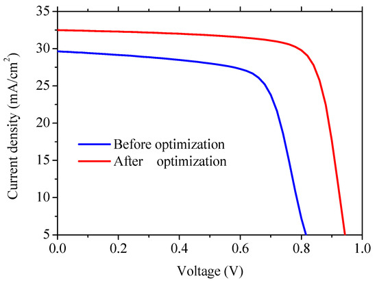
Figure 17.
J-V characteristics before and after optimization.
4. Conclusions
In this paper, lead-free PSCs with the MASnI3 perovskite as the absorber layer are investigated through SCAPS simulation. At first, optimal materials for the ETL and HTL are determined, which are Cd0.5Zn0.5S and MASnBr3, respectively. The suitability of those materials is shown by the appropriate band alignment between the CB level of Cd0.5Zn0.5S and MASnI3 and between the VB level of MASnI3 and MASnBr3. Next, the effects of absorber layer thickness, defect density in the absorber layer, defect density in interface layers, doping density in ETL and HTL, back-contact work function, and operation temperature on the PSC performance are discussed. The configuration of the PSC is glass substrate/FTO/Cd0.5Zn0.5S/MASnI3/MASnBr3/Au. Simulation results reveal that the optimal absorber layer thickness is 500 nm and a thinner absorber layer will lead to poor cell performance due to the insufficient photon absorption. An optimal defect density (1015 cm−3) in the absorber layer is found from the simulations, and any defect densities higher than that level will lead to the reduction of the solar cell performance due to the creation of additional recombination centers. It is confirmed that the defect densities in IL1 and IL2 should be less than 1015 and 1017 cm−3, respectively. Simulation results also indicate that the conductivities of ETL and HTL will improve when their doping densities increase. Finally, it is found that the solar cell performance will be impeded if the back-contact work function is less than 4.9 eV and the operating temperature is higher than 300 K. The results obtained from this study will facilitate the design of lead-free and efficient PSCs, therefore promoting the application of solar power as a form of sustainable energy along with wave energy [42,43] and wind energy [44,45]. Other factors that impact PSC performance such as the mobility and bandgap of perovskites will be investigated in the next phase of this project.
Author Contributions
Y.G. and X.B. conceived of the presented idea, they developed the device structure and carried out the numerical analysis. B.Q. investigated the effects of ETL and HTL materials on cell performance; Q.L. investigated the effects of absorber layer on cell performance; Q.J. studied the effects of interface layers on cell performance; and P.M. found out the effects of doping density, back-contact work function, and operating temperature on cell performance. Y.L. conducted the literature review and supervised the findings of this work. All authors contributed to the final version of the manuscript. All authors have read and agreed to the published version of the manuscript.
Funding
This research was funded by Guangxi Natural Science Foundation—Youth Fund Program (2019GXNSFBA245076) and the high-quality talents research startup fund from the Yulin Normal University (G2019ZK24).
Acknowledgments
The authors are grateful to Marc Bergelman from the University of Gent for providing the SCAPS simulation program.
Conflicts of Interest
The authors declare no conflict of interest. The funders had no role in the design of the study; in the collection, analyses, or interpretation of data; in the writing of the manuscript, or in the decision to publish the results.
References
- Eperon, G.E.; Burlakov, V.M.; Docampo, P.; Goriely, A.; Snaith, H.J. Morphological Control for High Performance, Solution-Processed Planar Heterojunction Perovskite Solar Cells. Adv. Funct. Mater. 2014, 24, 151–157. [Google Scholar] [CrossRef]
- Liu, M.; Johnston, M.B.; Snaith, H.J. Efficient planar heterojunction perovskite solar cells by vapour deposition. Nat. Cell Biol. 2013, 501, 395–398. [Google Scholar] [CrossRef]
- Conings, B.; Drijkoningen, J.; Gauquelin, N.; Babayigit, A.; D’Haen, J.; D’Olieslaeger, L.; Ethirajan, A.; Verbeeck, J.; Manca, J.; Mosconi, E.; et al. Intrinsic Thermal Instability of Methylammonium Lead Trihalide Perovskite. Adv. Energy Mater. 2015, 5, 1500477. [Google Scholar] [CrossRef]
- Wang, R.; Mujahid, M.; Duan, Y.; Wang, Z.; Xue, J.; Yang, Y. A Review of Perovskites Solar Cell Stability. Adv. Funct. Mater. 2019, 29. [Google Scholar] [CrossRef]
- Wang, Q.; Phung, N.; Di Girolamo, D.; Vivo, P.; Abate, A. Enhancement in lifespan of halide perovskite solar cells. Energy Environ. Sci. 2019, 12, 865–886. [Google Scholar] [CrossRef]
- Zheng, S.; Wang, G.; Liu, T.; Lou, L.; Xiao, S.; Yang, S. Materials and structures for the electron transport layer of efficient and stable perovskite solar cells. Sci. China Ser. B Chem. 2019, 62, 800–809. [Google Scholar] [CrossRef]
- Li, C.; Yang, X.; Zhao, Y.; Zhang, P.; Tu, Y.; Li, Y. Hole extraction layer utilizing well defined graphene oxide with multiple functionalities for high-performance bulk heterojunction solar cells. Org. Electron. 2014, 15, 2868–2875. [Google Scholar] [CrossRef]
- Liang, J.; Liu, J.; Jin, Z. All-Inorganic Halide Perovskites for Optoelectronics: Progress and Prospects. Sol. RRL 2017, 1, 1700086. [Google Scholar] [CrossRef]
- Yang, T.C.-J.; Fiala, P.; Jeangros, Q.; Ballif, C. High-Bandgap Perovskite Materials for Multijunction Solar Cells. Joule 2018, 2, 1421–1436. [Google Scholar] [CrossRef]
- Chen, H.; Xiang, S.; Li, W.; Liu, H.; Zhu, L.; Yang, S. Inorganic Perovskite Solar Cells: A Rapidly Growing Field. Sol. RRL 2018, 2, 1700188. [Google Scholar] [CrossRef]
- Song, T.-B.; Yokoyama, T.; Aramaki, S.; Kanatzidis, M.G. Performance Enhancement of Lead-Free Tin-Based Perovskite Solar Cells with Reducing Atmosphere-Assisted Dispersible Additive. ACS Energy Lett. 2017, 2, 897–903. [Google Scholar] [CrossRef]
- Green, M.A.; Ho-Baillie, A.; Snaith, H.J. The emergence of perovskite solar cells. Nat. Photon. 2014, 8, 506–514. [Google Scholar] [CrossRef]
- Kojima, A.; Teshima, K.; Shirai, Y.; Miyasaka, T. Organometal Halide Perovskites as Visible-Light Sensitizers for Photovoltaic Cells. J. Am. Chem. Soc. 2009, 131, 6050–6051. [Google Scholar] [CrossRef]
- Baig, F.; Khattak, Y.H.; Marí, B.; Beg, S.; Ahmed, A.; Khan, K. Efficiency Enhancement of CH3NH3SnI3 Solar Cells by Device Modeling. J. Electron. Mater. 2018, 47, 5275–5282. [Google Scholar] [CrossRef]
- Chen, M.; Ju, M.-G.; Carl, A.D.; Zong, Y.; Grimm, R.L.; Gu, J.; Zeng, X.C.; Zhou, Y.; Padture, N.P. Cesium Titanium(IV) Bromide Thin Films Based Stable Lead-free Perovskite Solar Cells. Joule 2018, 2, 558–570. [Google Scholar] [CrossRef]
- Chakraborty, K.; Choudhury, M.G.; Paul, S. Numerical study of Cs2TiX6 (X = Br−, I−, F− and Cl−) based perovskite solar cell using SCAPS-1D device simulation. Sol. Energy 2019, 194, 886–892. [Google Scholar] [CrossRef]
- Islam, M.; Rahman, K.; Misran, H.; Asim, N.; Hossain, M.; Akhtaruzzaman, M.; Amin, N. High mobility and transparent ZTO ETM prepared by RF reactive co-sputtering for perovskite solar cell application. Results Phys. 2019, 14, 102518. [Google Scholar] [CrossRef]
- Lakhdar, N.; Hima, A. Electron transport material effect on performance of perovskite solar cells based on CH3NH3GeI3. Opt. Mater. 2020, 99, 109517. [Google Scholar]
- Azri, F.; Meftah, A.; Sengouga, N.; Meftah, A. Electron and hole transport layers optimization by numerical simulation of a perovskite solar cell. Sol. Energy 2019, 181, 372–378. [Google Scholar] [CrossRef]
- Sajid, S.; Elseman, A.M.; Ji, J.; Dou, S.; Huang, H.; Cui, P.; Wei, D.; Li, M. Novel hole transport layer of nickel oxide composite with carbon for high-performance perovskite solar cells. Chin. Phys. B 2018, 27. [Google Scholar] [CrossRef]
- Minemoto, T.; Murata, M. Impact of work function of back contact of perovskite solar cells without hole transport material analyzed by device simulation. Curr. Appl. Phys. 2014, 14, 1428–1433. [Google Scholar] [CrossRef]
- Teimouri, R.; Mohammadpour, R. Potential application of CuSbS 2 as the hole transport material in perovskite solar cell: A simulation study. Superlattices Microstruct. 2018, 118, 116–122. [Google Scholar] [CrossRef]
- Niemegeers, M.; Burgelman, K.; Decock, J.; Verschraegen, S. Degrave, SCAPS Manual, version: 20 May 2014. Available online: http://scaps.elis.ugent.be (accessed on 1 November 2020).
- Lin, L.-Y.; Jiang, L.-Q.; Fan, B.-D. Analysis of Sb2Se3/CdS based photovoltaic cell: A numerical simulation approach. J. Phys. Chem. Solids 2018, 122, 19–24. [Google Scholar] [CrossRef]
- Lin, L.; Jiang, L.; Li, P.; Fan, B.; Qiu, Y. A modeled perovskite solar cell structure with a Cu2O hole-transporting layer enabling over 20% efficiency by low-cost low-temperature processing. J. Phys. Chem. Solids 2019, 124, 205–211. [Google Scholar] [CrossRef]
- Liu, X.; Yan, K.; Tan, D.; Liang, X.; Zhang, H.; Huang, W. Solvent Engineering Improves Efficiency of Lead-Free Tin-Based Hybrid Perovskite Solar Cells beyond 9%. ACS Energy Lett. 2018, 3, 2701–2707. [Google Scholar] [CrossRef]
- Guo, Y.; Jiang, J.; Zuo, S.; Shi, F.; Tao, J.; Hu, Z.; Hu, X.; Hu, G.; Yang, P.; Chu, J. RF sputtered CdS films as independent or buffered electron transport layer for efficient planar perovskite solar cell. Sol. Energy Mater. Sol. Cells 2018, 178, 186–192. [Google Scholar] [CrossRef]
- Qiu, W.; Buffière, M.; Brammertz, G.; Paetzold, U.W.; Froyen, L.; Heremans, P.; Cheyns, D. High efficiency perovskite solar cells using a PCBM/ZnO double electron transport layer and a short air-aging step. Org. Electron. 2015, 26, 30–35. [Google Scholar] [CrossRef]
- Chatterjee, S.; Pal, A.J. Introducing Cu2O Thin Films as a Hole-Transport Layer in Efficient Planar Perovskite Solar Cell Structures. J. Phys. Chem. C 2016, 120, 1428–1437. [Google Scholar] [CrossRef]
- Gharibzadeh, S.; Nejand, B.A.; Moshaii, A.; Mohammadian, N.; Alizadeh, A.H.; Mohammadpour, R.; Ahmadi, V.; Alizadeh, A. Two-Step Physical Deposition of a Compact CuI Hole-Transport Layer and the Formation of an Interfacial Species in Perovskite Solar Cells. ChemSusChem 2016, 9, 1929–1937. [Google Scholar] [CrossRef]
- Christians, J.A.; Fung, R.C.M.; Kamat, P.V. An Inorganic Hole Conductor for Organo-Lead Halide Perovskite Solar Cells. Improved Hole Conductivity with Copper Iodide. J. Am. Chem. Soc. 2014, 136, 758–764. [Google Scholar] [CrossRef]
- Qin, P.; Tanaka, S.; Ito, S.; Tetreault, N.; Manabe, K.; Nishino, H.; Nazeeruddin, M.K.; Graetzel, M. Inorganic hole conductor-based lead halide perovskite solar cells with 12.4% conversion efficiency. Nat. Commun. 2014, 5, 3834. [Google Scholar] [CrossRef] [PubMed]
- Jung, M.; Kim, Y.C.; Jeon, N.J.; Yang, W.S.; Seo, J.; Noh, J.H.; Seok, S.I. Thermal Stability of CuSCN Hole Conductor-Based Perovskite Solar Cells. ChemSusChem 2016, 9, 2592–2596. [Google Scholar] [CrossRef]
- Subbiah, A.S.; Halder, A.; Ghosh, S.; Mahuli, N.; Hodes, G.; Sarkar, S.K. Inorganic Hole Conducting Layers for Perovskite-Based Solar Cells. J. Phys. Chem. Lett. 2014, 5, 1748–1753. [Google Scholar] [CrossRef] [PubMed]
- Tanaka, K.; Minemoto, T.; Takakura, H. Analysis of heterointerface recombination by Zn1−xMgxO for window layer of Cu(In,Ga)Se2 solar cells. Sol. Energy 2009, 83, 477–479. [Google Scholar] [CrossRef]
- Turcu, M.; Rau, U. Fermi level pinning at CdS/Cu(In,Ga)(Se,S)2 interfaces: Effect of chalcopyrite alloy composition. J. Phys. Chem. Solids 2003, 64, 1591–1595. [Google Scholar] [CrossRef]
- Minemoto, T.; Murata, M. Theoretical analysis on effect of band offsets in perovskite solar cells. Sol. Energy Mater. Sol. Cells 2015, 133, 8–14. [Google Scholar] [CrossRef]
- Tan, K.; Lin, P.; Wang, G.; Liu, Y.; Xu, Z.; Lin, Y. Controllable design of solid-state perovskite solar cells by SCAPS device simulation. Solid State Electron. 2016, 126, 75–80. [Google Scholar] [CrossRef]
- Du, H.-J.; Wang, W.-C.; Zhu, J.-Z. Device simulation of lead-free CH 3 NH 3 SnI 3 perovskite solar cells with high efficiency. Chin. Phys. B 2016, 25, 108802. [Google Scholar] [CrossRef]
- Devi, N.; Parrey, K.A.; Aziz, A.; Datta, S. Numerical simulations of perovskite thin-film solar cells using a CdS hole blocking layer. J. Vac. Sci. Technol. B 2018, 36, 04G105. [Google Scholar] [CrossRef]
- Adhikari, K.R.; Gurung, S.; Bhattarai, B.K.; Soucase, B.M. Comparative study on MAPbI3 based solar cells using different electron transporting materials. Phys. Status Solidi (c) 2015, 13, 13–17. [Google Scholar] [CrossRef]
- Guiberteau, K.; Liu, Y.; Lee, J.; Kozman, T.A. Investigation of Developing Wave Energy Technology in the Gulf of Mexico. Distrib. Gener. Altern. Energy J. 2012, 27, 36–52. [Google Scholar] [CrossRef]
- Pastor, J.; Liu, Y. Hydrokinetic Energy: Overview and it’s Renewable Energy Potential for the Gulf of Mexico. In Proceedings of the 2012 IEEE Green Technologies Conference, Tulsa, OK, USA, 19–20 April 2012; Institute of Electrical and Electronics Engineers (IEEE): Piscataway Township, NJ, USA; pp. 1–3. [Google Scholar]
- Liu, Y.; Chu, S.J. Advance application of wind technology in Louisiana. Int. J. Energy Eng. 2012, 2, 60–66. [Google Scholar] [CrossRef]
- Chu, S.J.; Liu, Y.-C. Prospects of wind energy and wind power in Louisiana. In Proceedings of the 2011 IEEE Green Technologies Conference, Baton Rouge, LA, USA, 14–15 April 2011. [Google Scholar]


Publisher’s Note: MDPI stays neutral with regard to jurisdictional claims in published maps and institutional affiliations. |
© 2020 by the authors. Licensee MDPI, Basel, Switzerland. This article is an open access article distributed under the terms and conditions of the Creative Commons Attribution (CC BY) license (http://creativecommons.org/licenses/by/4.0/).