1. Introduction
The nanostructures introduced onto the substrate or surface of optoelectronic devices, including light-emitting diodes [
1,
2] and photovoltaics [
3,
4], show not only their self-cleaning effect [
5,
6,
7,
8] but also the function of improving optical properties through their anti-reflection effect [
8,
9] and plasmonic effect [
3,
4,
10]. Polymer solar cells (PSCs), one of the optoelectronic devices, are very thin, lightweight, and capable of solution processes, which makes them popular as flexible energy harvesters [
11,
12]. To fabricate ultrathin PSCs, it is essential to apply an ultrathin polymer substrate (less than 5 µm in thickness) [
3,
13,
14,
15], which is a critical factor in determining the flexibility and power per weight of PSCs. As the thickness of the polymer substrate decreases, the flexibility and adhesion property to the three-dimensional (3D) surface increase so that it can be attached to textiles or human skin. Therefore, it can be applied as a power source such as an electrocardiogram sensor by sticking it on the human body [
3,
16]. By introducing nanostructures onto an ultrathin polymer substrate, including the previously mentioned effects, the power conversion efficiency (PCE) of PSCs is improved through the enhancement of optical properties, and the dependence on the incident angle is reduced [
17], so that it can be used as a stable power source for self-powered devices [
3].
The method of manufacturing nanostructures on ultrathin polymer substrates can be explained in two ways. The first is a dry etching method using direct laser interference patterning (DLIP) technology [
11,
18]. DLIP structures polymer substrates by direct ablation of the substrate material, depending on the required laser irradiation conditions [
18]. A grating pattern (U-shape) with a period of 1.8 µm was introduced on a 125 µm thick polyethylene terephthalate substrate, and the PCE w as improved by 16% compared to the non-patterned structure [
11]. The second method is soft nano-imprinting technology, applying a solution process. PCE was enhanced by 19% by applying a soft nano-imprinting technology on spin-coated ZnO using a soft mold such as poly(dimethylsiloxane) (PDMS), and forming nanostructures on the substrate surface [
19]. However, most studies have used flexible substrates with a thickness of 100 μm or more, and there have been few studies on patterned ultrathin substrate-based PSCs (less than 5 µm in thickness). In our previous study, we achieved a PCE of 10.26% by introducing a one-dimensional (1D) nanograting pattern with a period of 760 nm on a 1 μm-thick parylene substrate [
17]. However, since the ultrathin substrate was produced by the chemical vapor deposition process, it is not easy to fabricate a large-scale substrate and complicate the application of a roll-to-roll process.
To overcome this shortcoming, we report a new method to fabricate a patterned ultrathin substrate by an atmospheric pressure process. We prepared a 1D nanograting patterned template with a period of 760 nm and a height of 100 nm. To facilitate the peeling of the ultrathin polymer substrate from the 1D nanograting patterned template, we increased the hydrophobicity of the surface of the patterned template through self-assembly monolayer (SAM) treatment by using trichloro(perfluorooctyl)silane (FOTS). The ultrathin polymer substrate was applied to a poly (vinyl alcohol) (PVA)/epoxy (SU-8) double-layered structure and showed strong solvent resistance to various organic and polar solvents. By introducing a 1D nanograting pattern onto the ultrathin polymer substrate, the angular dependence of the ultrathin PSCs was significantly reduced from the incident angles of light. In addition, the triple-patterned ultrathin PSC having an ultrathin polymer substrate with a 1D nanograting pattern added onto both the electron transport layer and the photoactive layer showed a notable increase in PCE from 8.76% to 10.26%.
2. Materials and Methods
2.1. Preparation of 1D Nanograting-Patterned PDMS Mold
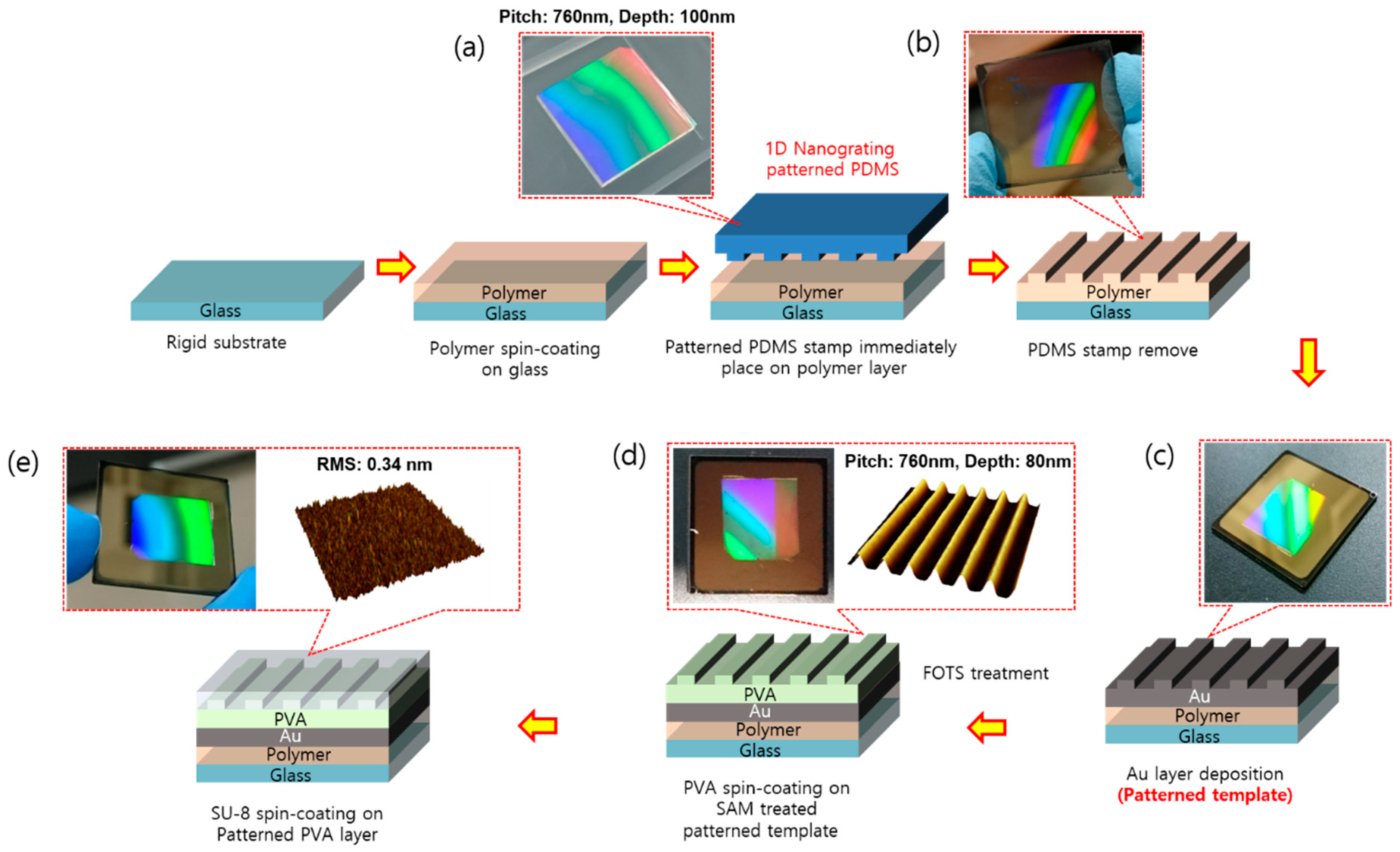
To introduce a 1D nanograting pattern to both the ZnO layer and photoactive layers, we prepared a 1D nanograting-patterned PDMS mold. The covered polycarbonate film of a blank DVD-RW (Sony, Tokyo, Japan) was manually peeled off using a surgical knife to create the grating pattern. To make a UV-curable PDMS mixture, the base polymer (X-34-4184A; Shin-Etsu, Tokyo, Japan) and the curing agent (X-34-4184 B; Shin-Etsu) were mixed in a 1:1 ratio. It was then degassed in a vacuum chamber for 10 min to remove air bubbles from the PDMS mixture completely. The prepared PDMS mixture was carefully poured onto the master mold, and the prepared sample was degassed again for 10 min. To solidify the PDMS, the sample was irradiated with UV light at 365 nm wavelength for 3 h, and the patterned PDMS mold was removed from the master mold. We achieved a 1D nanograting patterned PDMS mold with a pattern pitch of 760 nm and a height of 100 nm (
Figure 1a).
2.2. Fabrication of 1D Nanograting-Patterned Polymer Template (Patterned Template)
Bare glass (Corning) was washed by sequential sonication for 20 min each in detergent, deionized (DI) water, acetone, isopropyl alcohol, and DI water, and baked on a hot plate at 110 °C for 10 min. Ultraviolet-ozone (UVO) treatment was performed for 10 min to remove the residual chemicals on the bare glass. A polymer solution with a molecular weight of 30,000 or more, which is well-soluble in an organic solvent, was spin-coated (2000 rpm for 30 s) on the bare glass. Note that most of the polymers can be used, and in this experiment, the polymer used as the electron donor polymer (PBDTTT-OFT) of the photoactive layer in the PSCs was used for the 1D nanograting-patterned polymer template. After spin coating, the patterned PDMS mold was gently placed onto the photoactive layer immediately (within 5 s), and the PDMS mold was peeled off after 60 s. The patterned PDMS mold was very easily peeled off from the surface of the photoactive layer. Subsequently, a 1D nanograting pattern was achieved on the entire polymer layer (
Figure 1b). The glass substrate with the 1D nanograting-patterned polymer template was dried for approximately 1 h at 60 °C. To protect the surface of the 1D nanograting-patterned polymer template, a 50 nm-thick Au layer was deposited using a thermal evaporator (
Figure 1c). By introducing the Au protection layer, it can be used more than 50 times as the patterned template.
2.3. SAM Treatment Process
To decrease the surface energy of the 1D nanograting-patterned template, we introduced a perfluoro silane SAM such as FOTS (98%, Merck). Because of this, we could easily delaminate the patterned ultrathin substrate-based PSCs from the template. A 300 mL volume container was prepared, and the UVO treated (30 min, Ahtech LTS) template and a small chalet were placed in the container.
2.4. Fabrication of Patterned Ultrathin Substrate
A 3 and 6 wt% PVA (Mw: 186,000 g/mol, Merck) was dissolved in DI water for 6 h at 75 °C. A 1 um-thick PVA layer was spin-coated onto the SAM-treated 1D nanograting-patterned template at 3000 rpm for 60 s, and thermal annealing was performed on a hotplate at 60 °C for 60 min. The pattern pitch was 760 nm, and the height was 80 nm. (
Figure 1d).
To enhance the solvent resistance to the DI water, and to planarize the PVA layer, an epoxy (SU-8 3005, MicroChem) layer was introduced onto the PVA layer. A layer of 800 nm thick SU-8 was spin-coated (4500 rpm, 60 s). Then, it was prebaked for 3 min at 95 °C, followed by UV exposure and post-baking (for 3 min at 95 °C). The surface was flat with a root mean square of 0.34 nm, and the nanograting pattern was not observed (
Figure 1e).
2.5. Fabrication of Patterned Ultrathin Substrate-Based PSCs
A 100-nm thick layer of indium tine oxide (ITO) electrode was sputtered at room temperature. Subsequently, a 40 nm-thick ZnO layer was introduced as the electron-transporting layer. The ZnO nanoparticles (ZnO NPs) were prepared in the same way as in our previous study [
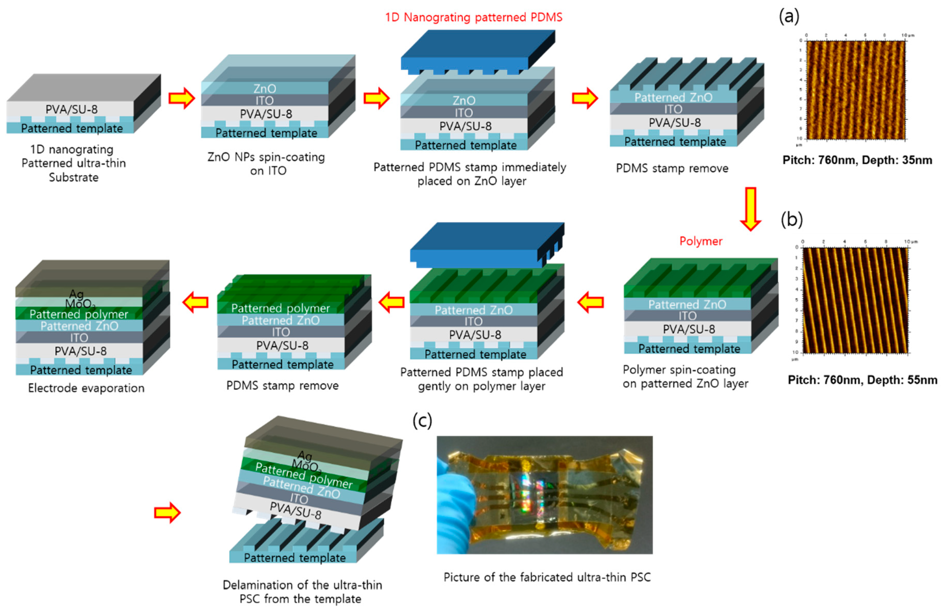
19]. To introduce a 1D nanograting pattern onto the surface of the ZnO layer, the patterned PDMS mold was quickly (within 5 s) placed on the ZnO layer without any additional pressure and thermal treatment. The patterned PDMS mold was eliminated after 60 s. The average depth and pattern pitch of the nanograting patterned ZnO layer were 35 and 760 nm, respectively.
To prepare the photoactive layer, PBDTTT-OFT and PC71BM mixture (ratio-1:1.5) was dissolved in chlorobenzene (1 mL) with 3 vol% 1,8-diiodooctane (DIO) (98%, Merck). To fabricate a 110 nm-thick photoactive layer, the prepared mixture solution was spin-coated on the electron-transporting layer at 800 rpm for 7 s.
Similar to the nanograting patterned ZnO layer, to introduce a 1D nanograting pattern on the photoactive layer, the patterned PDMS mold was placed on the photoactive layer without any additional pressure and thermal annealing process.
The prepared sample was transferred to a thermal evaporator to form metal electrodes. A MoO3 hole-transporting layer (0.1 °A s−1, 2 nm) and Ag electrodes (0.5 °A s−1, 80 nm) were thermally deposited by an evaporator under a high vacuum (below 5 × 10⁻⁵ Torr) using a metal mask.
2.6. Measurements
The film thickness of the photoactive layer and the ZnO layer was measured by surface profiler (DEKTAK 6M, Bruker, Billerica, MA, USA). The water contact angle measurement was conducted using a DAS 100 (KRUSS) measurement system. The absorption and transmission measurements were performed using UV-Vis spectroscopy (V-670, JASCO, Oklahoma, OK, USA). The surface morphology images of the 1D nanograting patterned ZnO and photoactive layers were observed by AFM (5400, Agilent Technologies, Santa Clara, CA, USA).
The current density–voltage (J–V) characteristics of the PSCs were measured using a source measurement unit (2400, Keithley). The PSCs were evaluated using a solar simulator (PEC-L11, Peccell Technologies, 150 W Xe lamp) under simulated solar illumination (Air Mass1.5G, 100 mW cm−2) at 298 K. The active area of the PSCs was 0.12 cm2. The external quantum efficiency (EQE) of the PSCs was measured using SM-250F monochromator (Bunkoh-Keiki, Tokyo, Japan).
For the angle dependence experiments, the J–V characteristics of the PSCs were measured while changing the incident angle of light by 10° from 0° to 80° under illumination.
3. Results and Discussions
Figure 1 shows a schematic illustration of the procedure used to introduce the 1D nanograting patterns to the ultrathin polymer layer by soft nano-imprinting technology using a PDMS mold. The detailed process is shown in the experimental section (see
Section 2.1,
Section 2.2,
Section 2.3 and
Section 2.4).
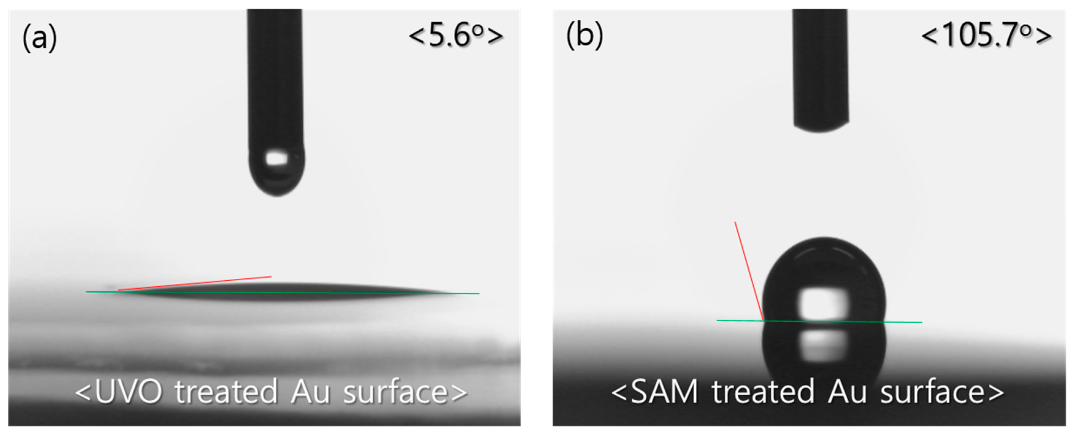
To easily delaminate the thin-film polymer substrate from the patterned template, a SAM treatment using FOTS was performed. As shown in
Figure 2, the water contact angle of the FOTS-treated patterned template was improved to 105.7°. It can be confirmed that the substrate has been changed to hydrophobic, which means that the surface energy of the SAM-treated patterned template is lower than that of the non-treated patterned template.
Figure 3a shows the transmittance of the various PVA ultrathin films. The transmittances of 3% and 6% PVA with glass and bare glass were almost similar. This means that PVA has no optical interference with the glass substrate and exhibits very high transmittance. Interestingly, the transmittance of the PVA free-standing film in the UV region is very significant. Therefore, it is considered that the application as a UV-detecting sensor with PVA as an ultrathin substrate is also possible.
In addition, a solvent resistance test was conducted on the PVA ultrathin film (
Figure 3b). The ultrathin PVA film showed strong solvent resistance to common organic solvents. However, as expected, the solvent resistance to DI water was insufficient.
To solve this problem, we introduced SU-8, an epoxy-based photocurable material, on top of the PVA layer. As shown in
Figure 3c, we confirmed that the solvent resistance to DI water, as well as common organic solvents, was excellent. Therefore, by introducing the SU-8 layer, the photolithography process became possible. Interestingly, since the SU-8 layer does not reflect the surface shape of the underlying nanograting patterned PVA, the surface roughness was reduced to 0.34 nm. This would lead to an improvement in the characteristics of organic electronic devices sensitive to surface roughness. In the case of the PVA/SU-8 double-layered free-standing film, the transmittance in the UV region decreased (
Figure 3d). This is due to the inherent properties of epoxy-based polymers.
A schematic illustration of the patterned ultrathin PSCs with an ultrathin nanograting polymer substrate is presented in
Figure 4. We introduced 1D nanograting patterns to both the surface ZnO layer and the photoactive layer in PSCs by soft nano-imprinting lithography using a PDMS mold. The ultrathin device structure was PVA/SU-8 (1.8 um)/ITO (100 nm)/ZnO NPs (with/without the pattern, about 40 nm)/photoactive (with/without the pattern, 110 nm)/MoO
3 (2 nm)/Ag electrode (80 nm). The period of the 1D nanograting pattern applied to the PSCs is 760 nm, which is the same as the pattern pitch applied to the ultrathin substrate. Even after the vacuum deposition of the metal electrode, the nanopattern has remained on the Ag electrode surface because the MoO3/Ag layer was thin enough to reflect the nanostructure of the surface present in the underlying layer. (inset in
Figure 4).
Figure 5 presents the current density–voltage (J–V) characteristics of PBDTTT-OFT: PC
71BM-based PSCs fabricated using three kinds of device structures. The short circuit current density (J
SC), open-circuit voltage (V
OC), fill factor (FF), and PCE of the devices are presented in
Table 1. Introducing the nanograting pattern onto the ultrathin polymer substrate increased J
SC from 17.09 mA cm
−2 in the non-patterned device to 17.49 mA cm
−2 (
Figure 5a). Interestingly, introducing the nanopattern slightly increased FF; substrate patterned devices showed a higher FF of 72.1% than the non-patterned device (69.0%). As a result, the PCE was enhanced from 8.76% to 9.54%. In addition, introducing the nanograting patterns onto both the ZnO layer and the photoactive layer increased the J
SC further to 18.73 mA cm
−2 while maintaining a similar V
OC. This multiple increase in J
SC by the nanograting patterns resulted in a PCE of 10.26% for the triple-patterned PSC, which was the highest among the devices. The series resistance (R
S) and shunt resistance (R
SH) were obtained from the J–V curves (
Table 1). Introducing the nano structure led to a slight decrease in the R
S compared with the non-patterned PSC, whereas it increased the R
SH [
4].
To confirm the origin of the increase in J
SC, we measured the external quantum efficiency (EQE) of the PSCs (
Figure 5b). Due to the nanograting pattern applied to the ultrathin substrate, the EQE values in the 300–400 nm and 450–650 nm regions were improved. This improvement can be attributed to the anti-reflection effect and the increase in light path length, respectively [
4]. In addition, when nanograting patterns were introduced to both the ZnO layer and photoactive layer, an EQE increase in the entire wavelength region was observed. This can be attributed to the surface plasmon resonance effect between the patterned photoactive layer and the metal electrode.
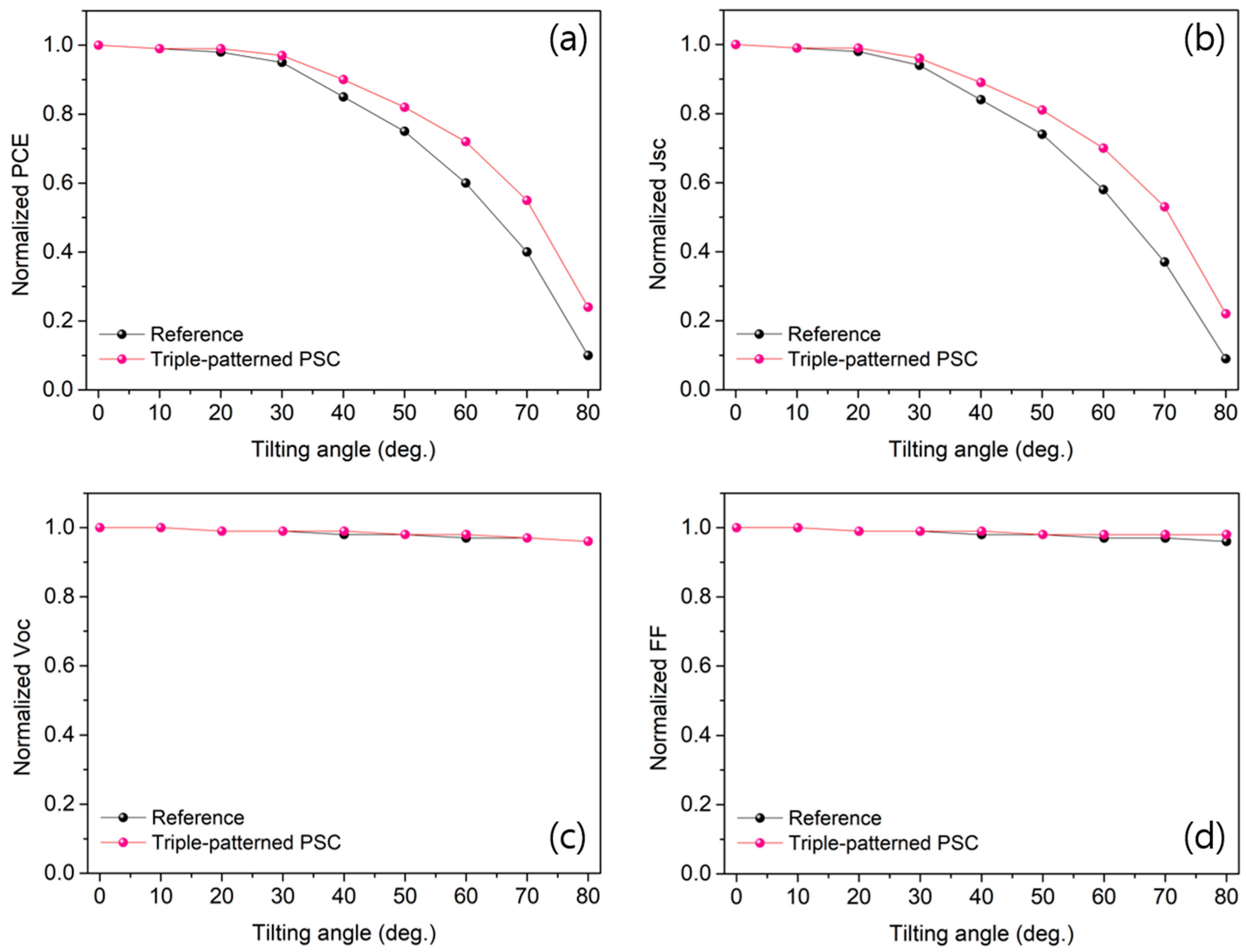
In addition to high PCE, the triple-patterned PSCs using patterned ultrathin polymer substrates show a lower dependence on the incident angle of light.
Figure 6a shows the PCE with the incident angle of the light changed from 0° to 80°.
For the triple-patterned PSC with ultrathin nanograting polymer substrates, the decrease in normalized PCE was suppressed when the incident angles of light were changed compared to the reference device. In particular, the Jsc values were very sensitive to the changes in the incident angle of light, similar to the PCE value. In contrast, the triple-patterned PSCs do not affect the V
OC and FF, which remain almost unchanged regardless of the illumination angle, similar to the PSCs with the non-patterned substrates (
Figure 6c,d). As described above, since the PSCs with the triple-patterned structure are less dependent on the incident angle of light, they can be applied to biosensors attached to the human body or as a power source for mobile devices.
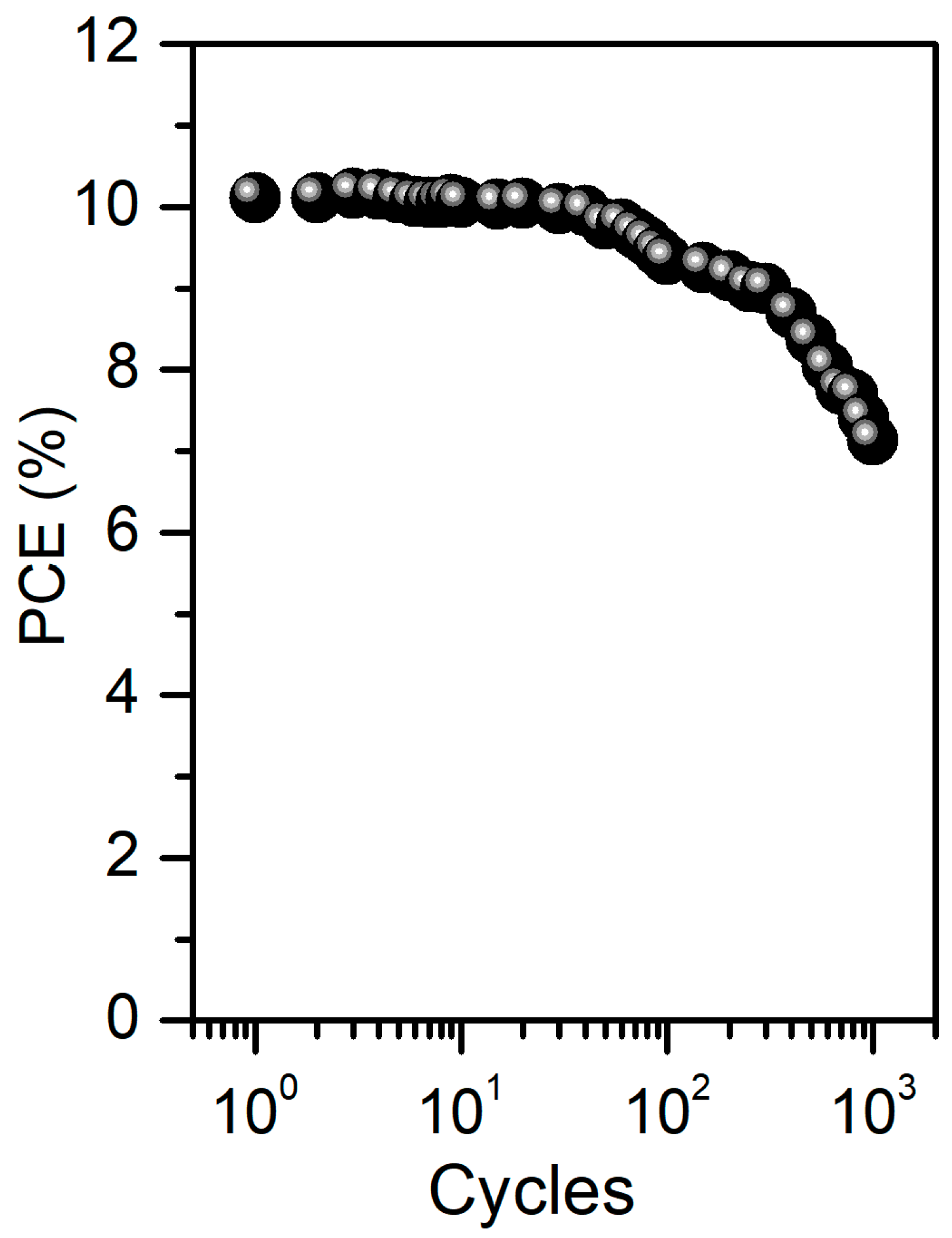
A compression test was performed to evaluate the mechanical properties of the triple-patterned PSCs. After delamination from the template, the triple-patterned PSCs were laminated onto a 200% pre-stretched elastomer film. Then, the devices were compressed in the uniaxial center direction by slowly reducing the stretching force, inducing a tensile strain in the elastomer film of 200–0%, which corresponded to the compression of the triple-patterned PSCs. The PCE decreased from 10.1% to 7.13% after 1000 repetitive compression cycles at 33% compression strain (
Figure 7). This excellent durability suggested that the triple-patterned PSCs can be utilized as power sources for mobile devices.
