Voltage-Balancing Strategy for Three-Level Neutral-Point-Clamped Cascade Converter under Sequence Smooth Modulation

Abstract
1. Introduction
- (1)
- High-voltage and high-power output can be realized by low-voltage power-switching devices;
- (2)
- The switching frequency of a single power-switching device is low;
- (3)
- Low loss of power-switching devices;
- (4)
- The filter device is physically small in size.
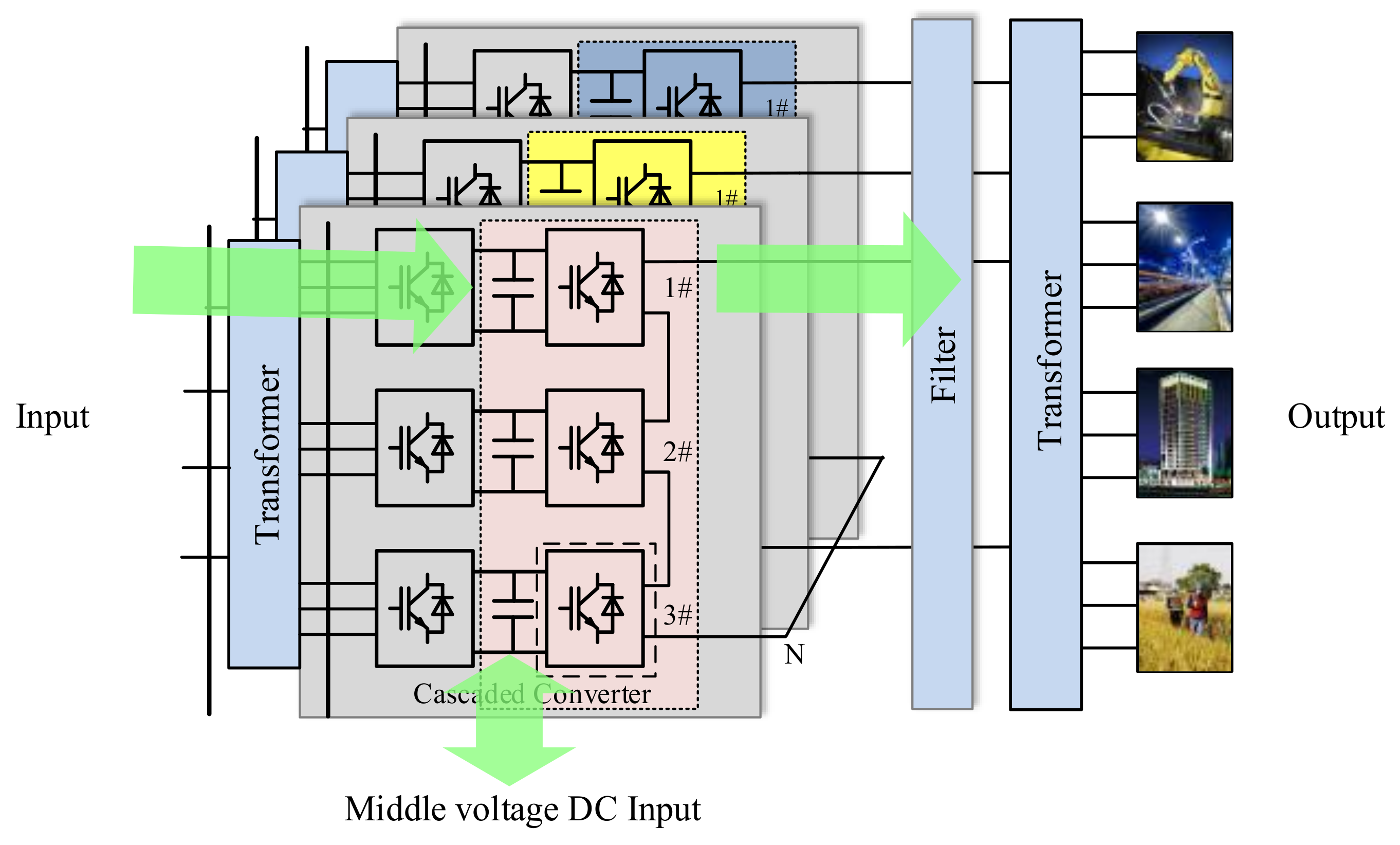
2. The Configuration and Control Strategy of 3LNPC-CC
2.1. The Configuration of the Multimodule 3LNPC-CC
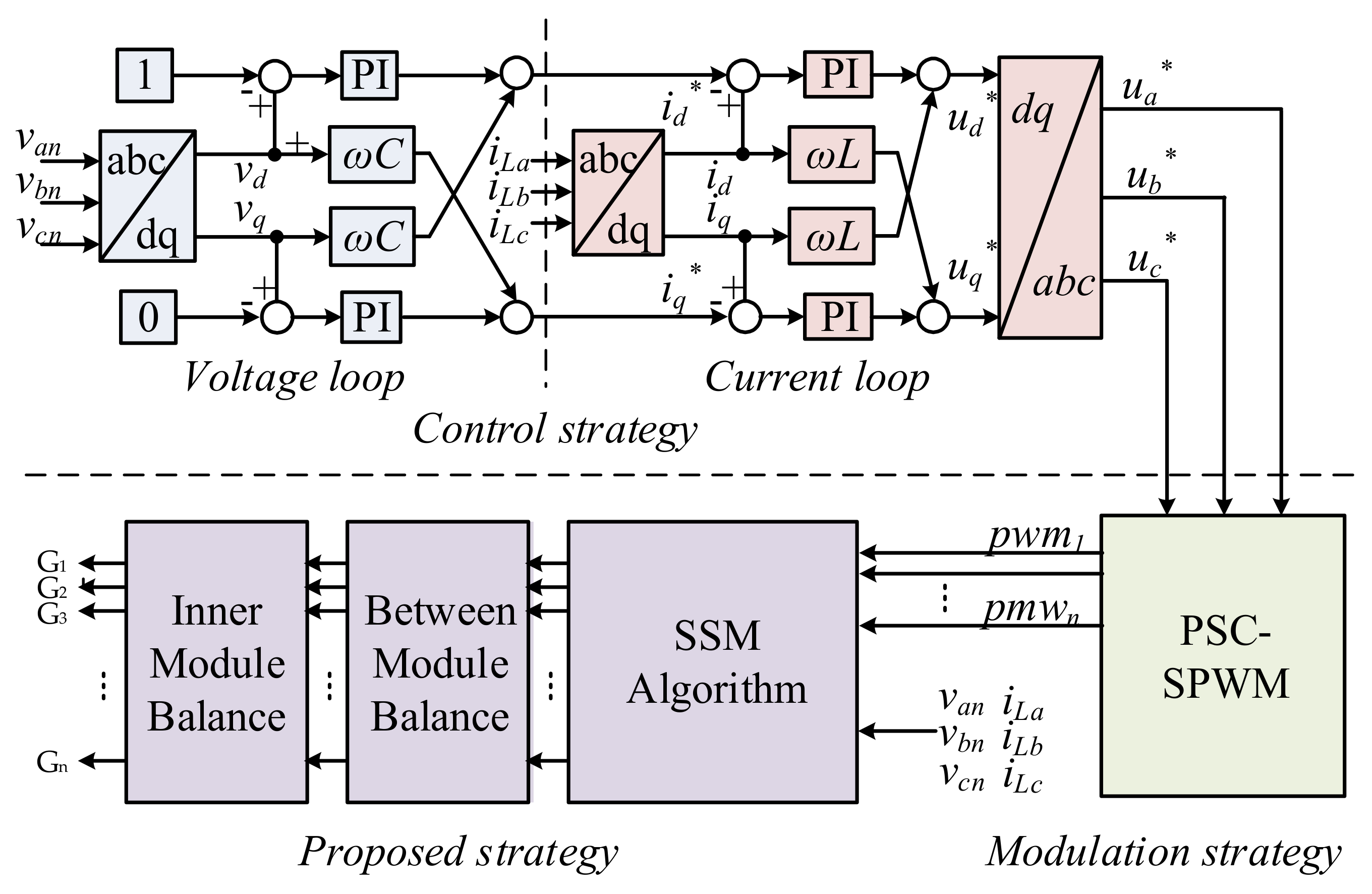
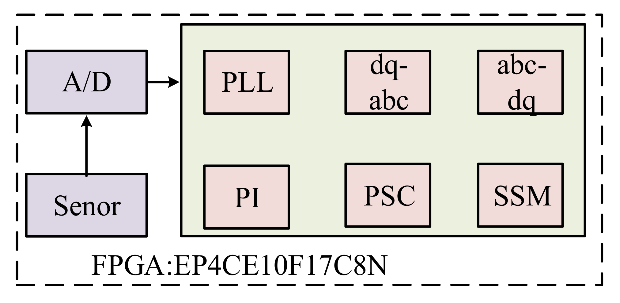
2.2. The Control Strategy of the Multimodule 3LNPC-CC
3. The Proposed Strategy of 3LNPC-CC
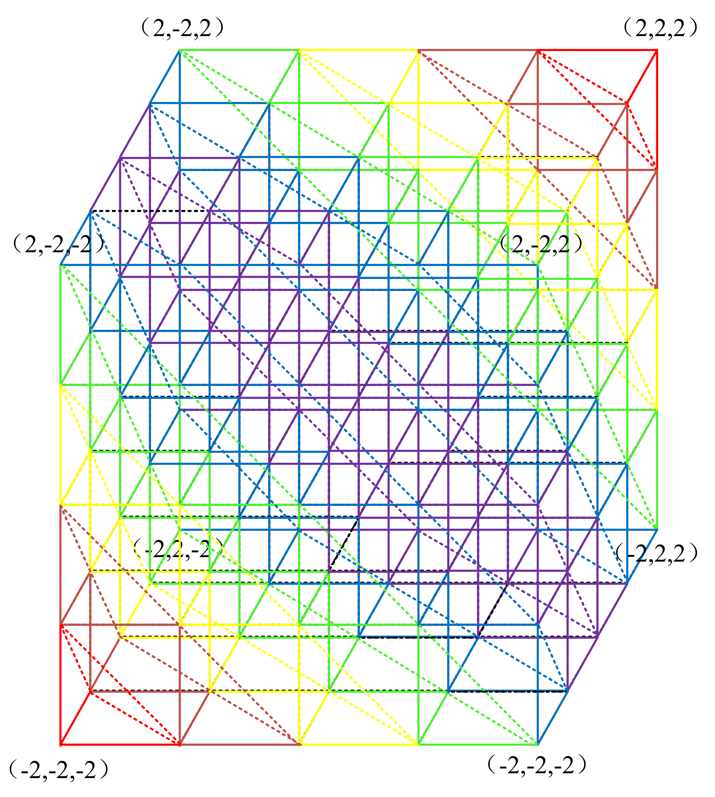
3.1. The Proposed Strategy
- (a)
- DC-side voltage rank: Vdc1> Vdc2> Vdc3, voltage level: positive plus, the number of module which the switch state is 2:0, initial example: (1,1,1), result example (2,1,1);
- (b)
- DC-side voltage rank: Vdc3> Vdc2> Vdc1, voltage level: positive plus, the switch state of Module 3 is 2, initial example:(1,1,2), result example (1,2,2);
- (c)
- DC- side voltage rank: Vdc2> Vdc3> Vdc1, voltage level: positive plus, the switch state of Module 3 is 2 and the switch state of Module 2 is 2, initial example:(−1,2,2), result example (0,2,2);
- (d)
- DC- side voltage rank: Vdc1> Vdc2> Vdc3, voltage level: positive minus, the number of module which the switch state is −2:0, initial example:(1,1,1), result example (1,1,0);
- (e)
- DC- side voltage rank: Vdc3> Vdc2> Vdc1, voltage level: positive minus, the switch state of Module 1 is −2, initial example:(1,2, −2), result example (1,1, −2);
- (f)
- DC- side voltage rank: Vdc1> Vdc2> Vdc3, voltage level: negative plus, the number of module which the switch state is 2:0, initial example:( −1, −1, −1), result example (−1, −1,0);
- (g)
- DC- side voltage rank: Vdc3> Vdc2> Vdc1, voltage level: negative plus, the switch state of Module 1 is 2, initial example:( −1, −1, −2), result example (−1,0, −2);
- (h)
- DC- side voltage rank: Vdc1> Vdc2> Vdc3, voltage level: negative minus, the number of module which the switch state is −2:0, initial example:( −1, −1, −1), result example (−1, −1, −2);
- (i)
- DC- side voltage rank: Vdc3> Vdc2> Vdc1, voltage level: negative minus, the switch state of Module 1 is −2, initial example: −2, −1, −1), result example (−2, −2, −1);
- (j)
- DC- side voltage rank: Vdc2> Vdc3> Vdc1, voltage level: negative minus, the switch state of Module 3 and Module 3 are −2, initial example:(−2, −2,1), result example (−2, −2,0);
- (k)
- The special situation; (2,2,2) cannot be added anymore, and the (−2, −2, −2) cannot be reduced any more.
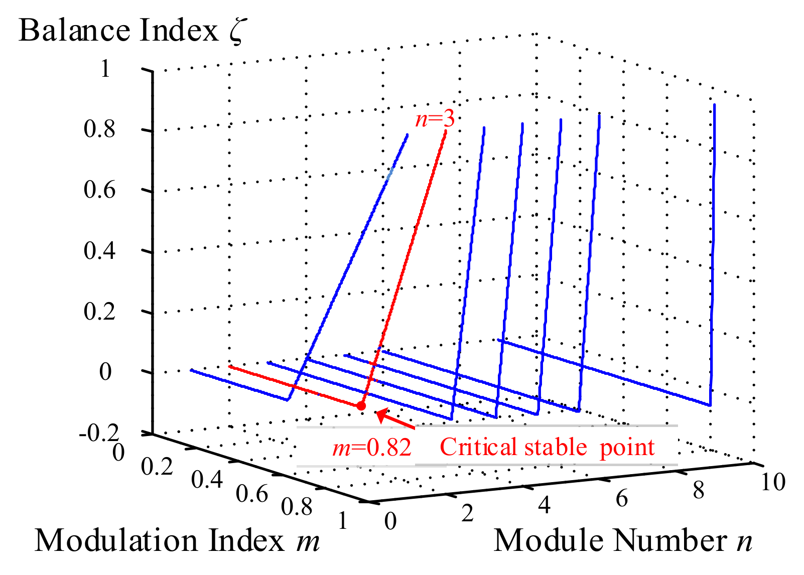
3.2. The Balance Range of the Proposed Strategy
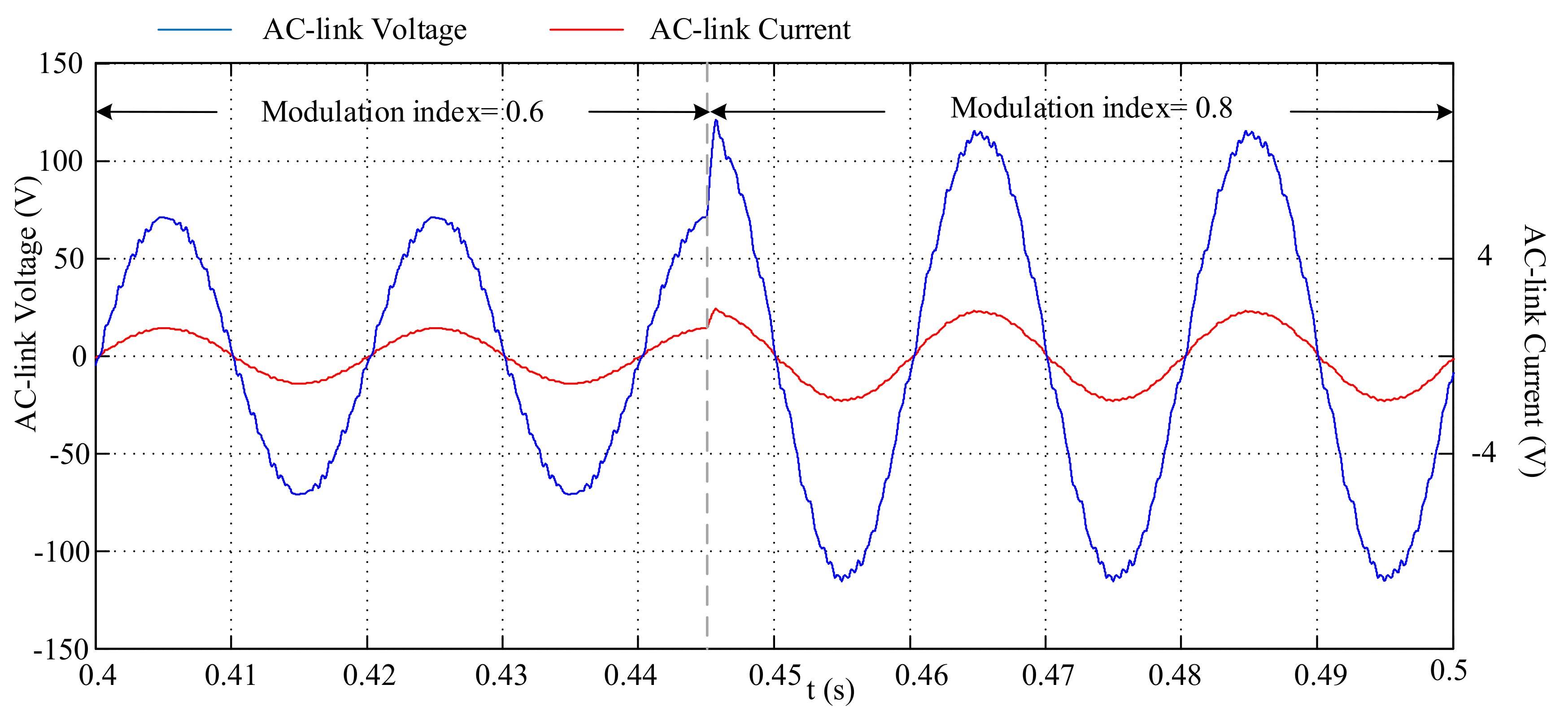
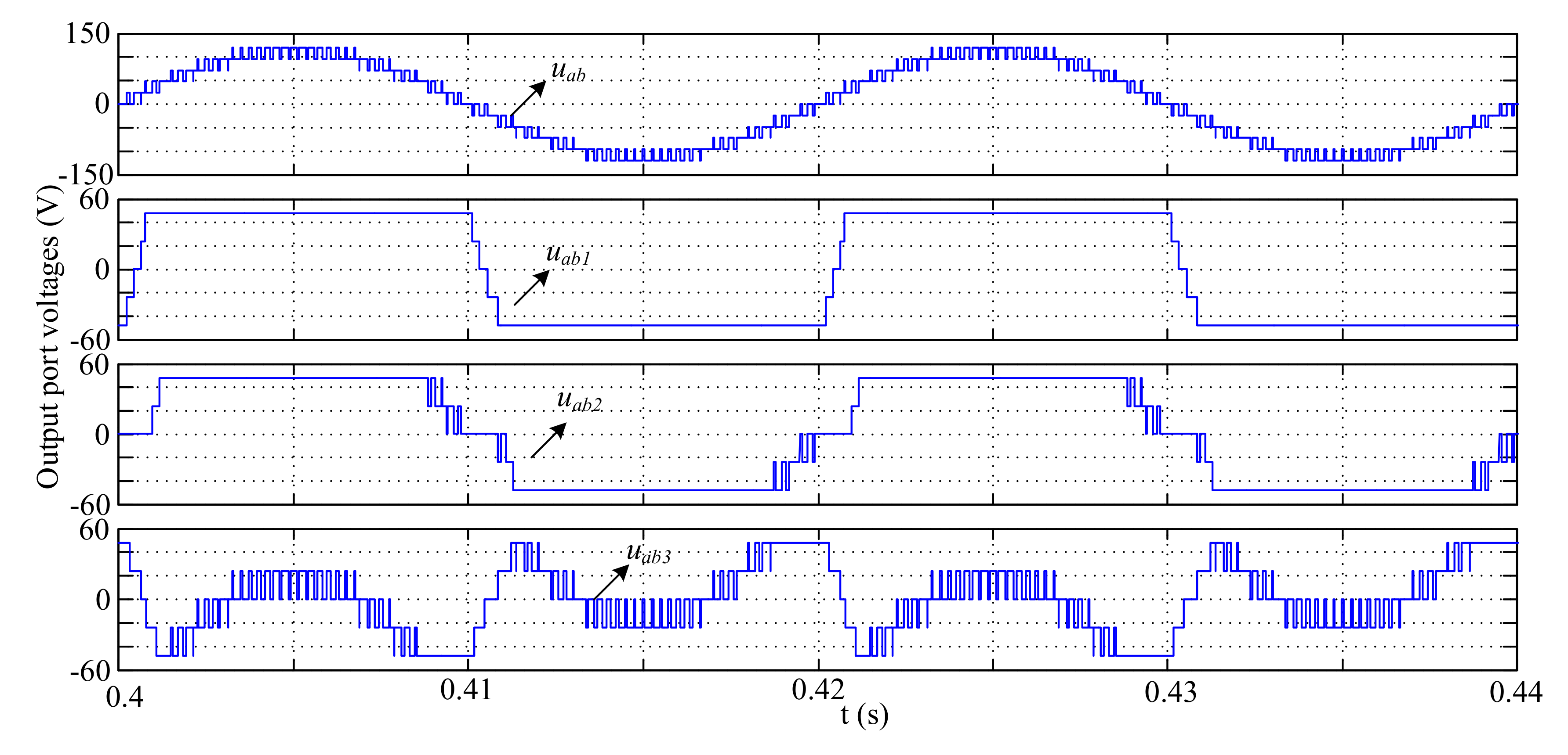
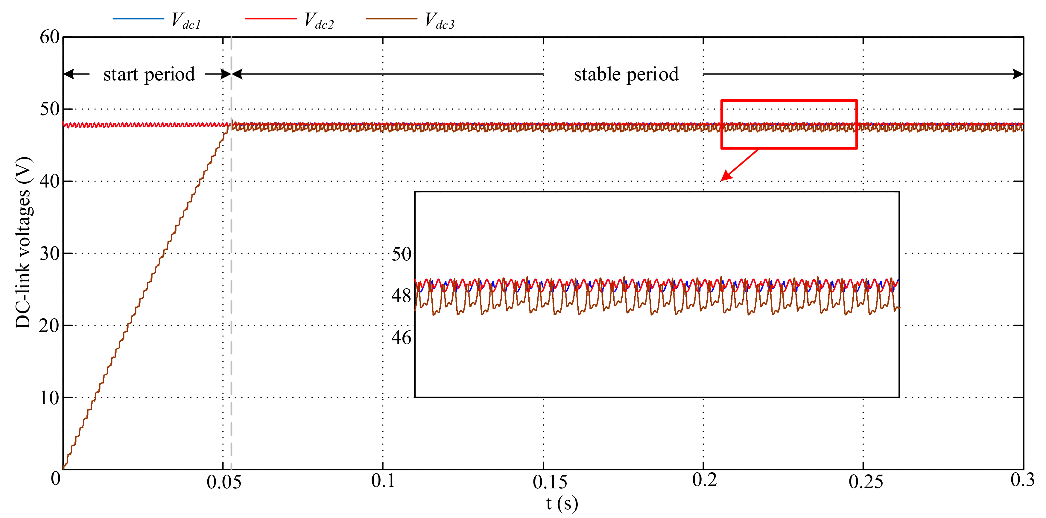
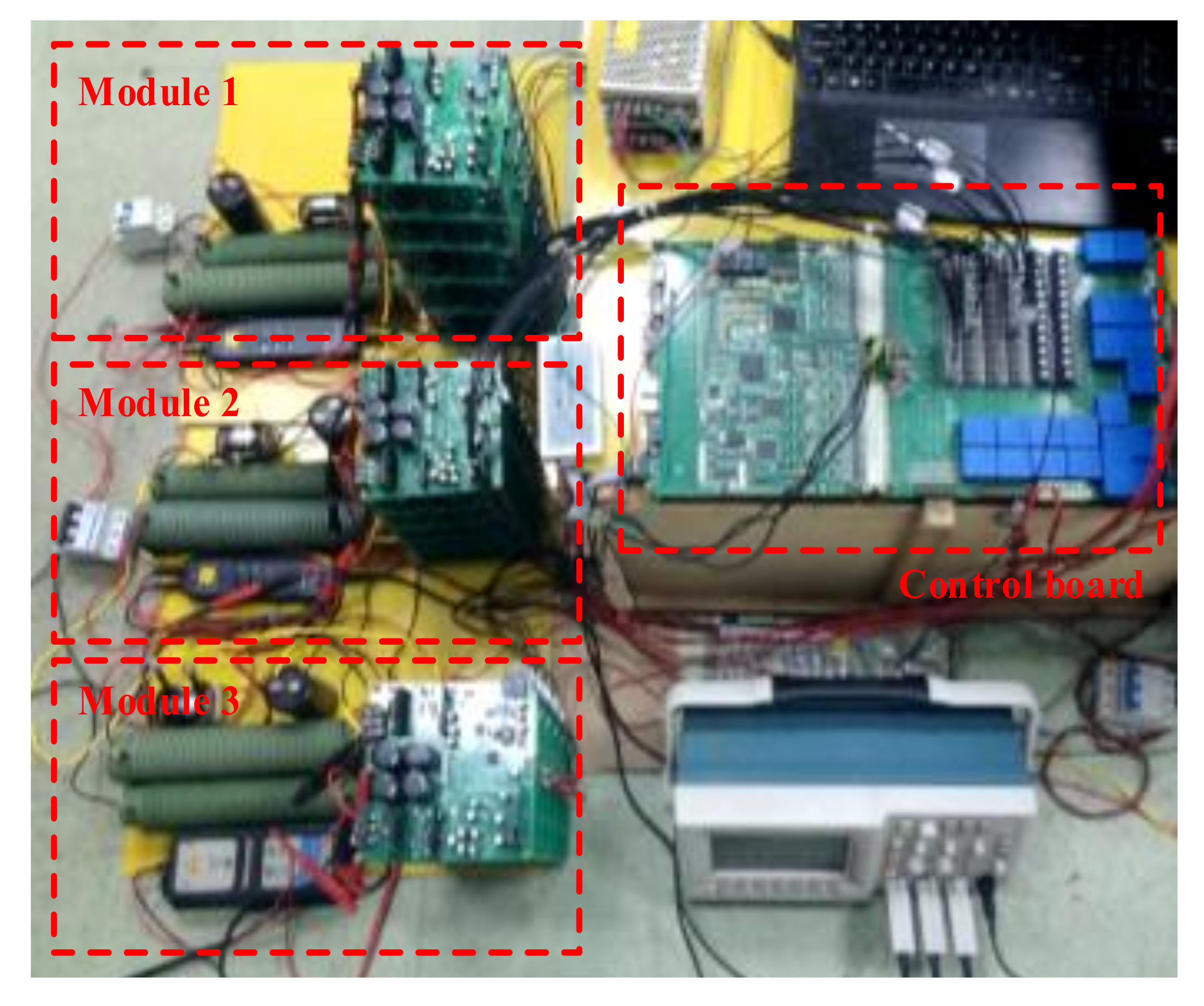
4. Simulation and Experiment
4.1. Simulation
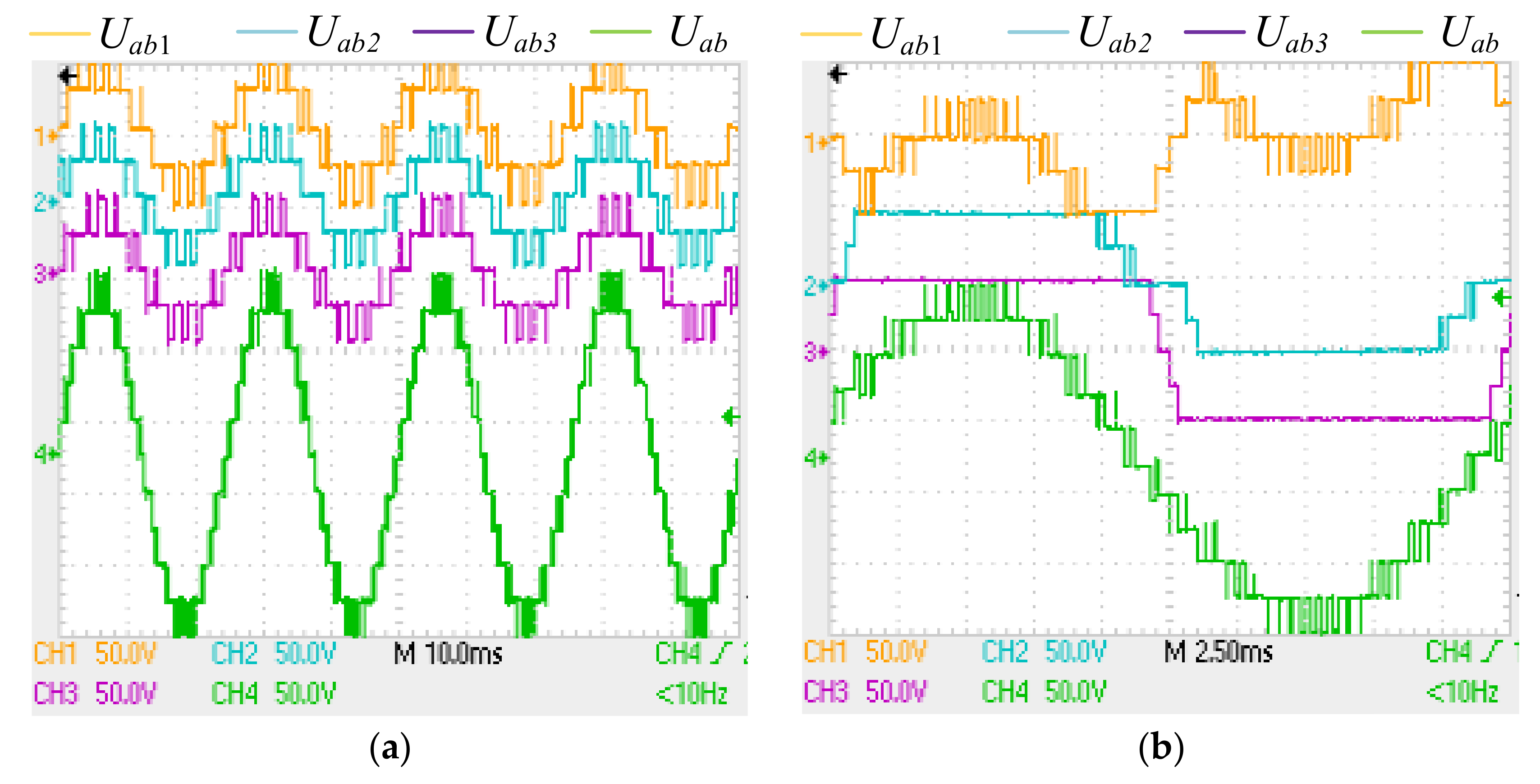
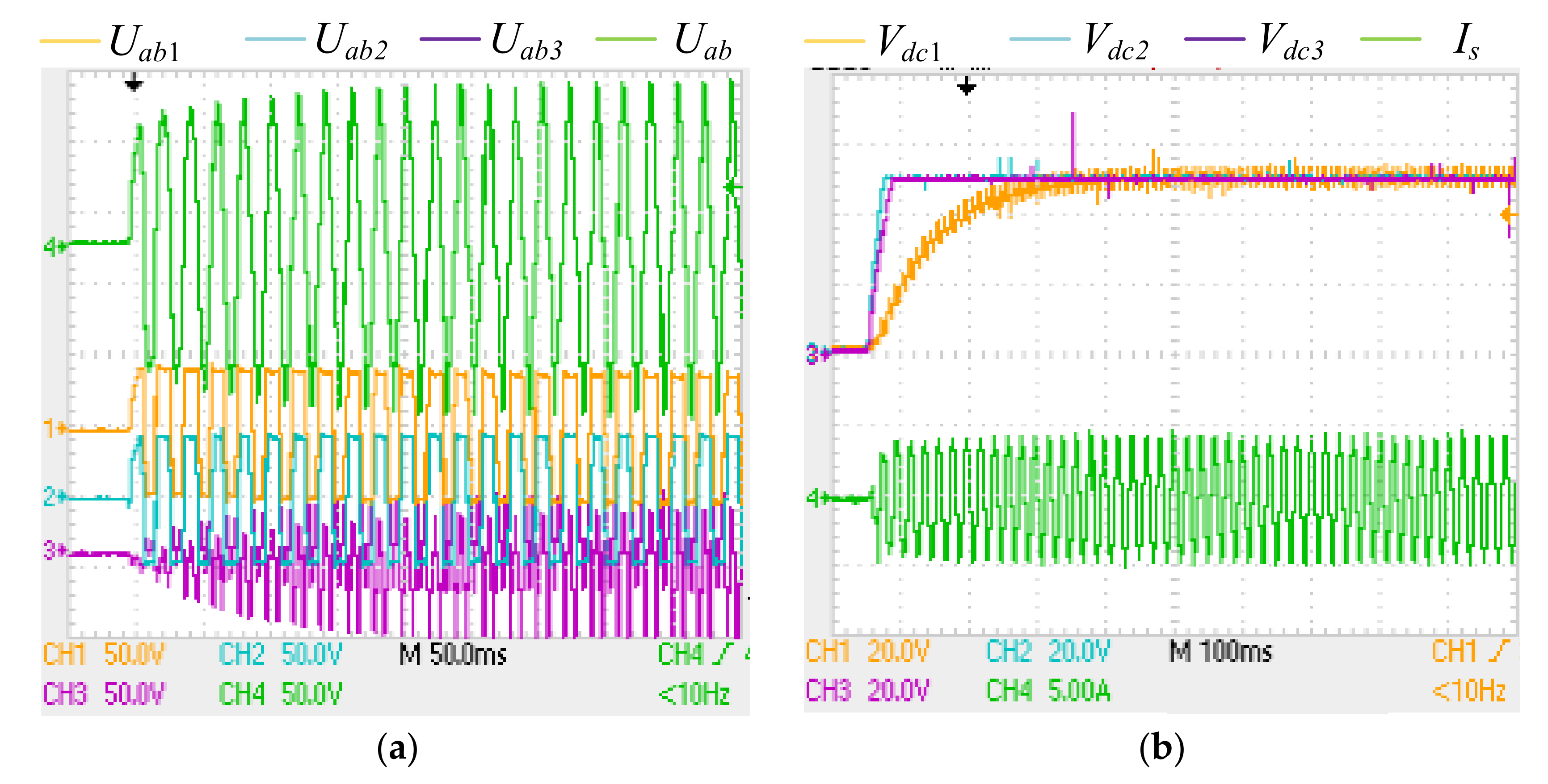
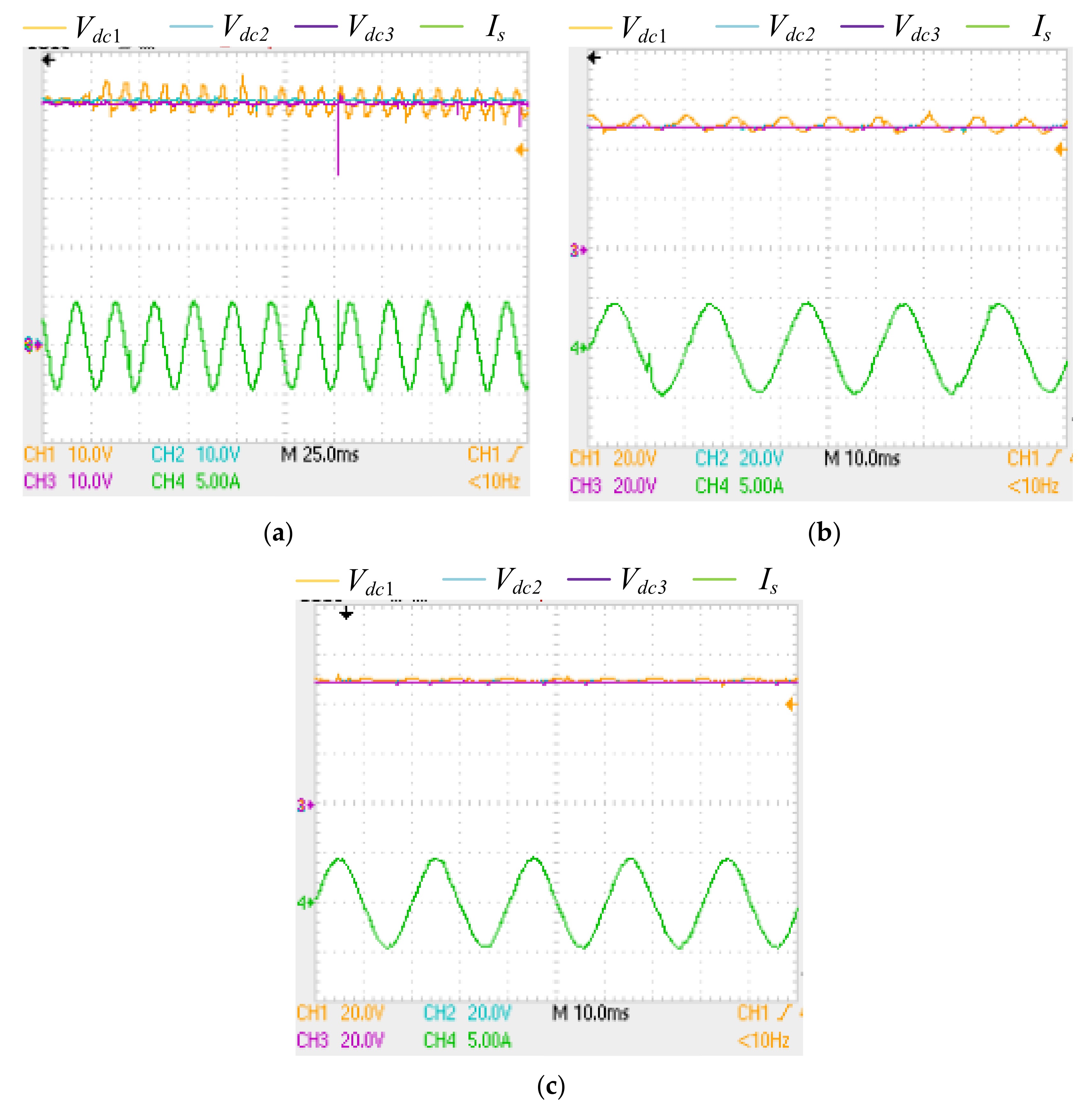
4.2. Experiment
5. Conclusions
- (a)
- An SSM structure of 3LNPC-CC is proposed, which represents the change of different working states. When the input of 3LNPC-CC is unbalanced, the normal path of working states is changed and an improved path of working states is assigned that can recover the balance of DC-side balance. The advantage of the improved path is a smooth switch of voltage level during the whole working cycle;
- (b)
- A coordinated control strategy is designed, which is composed of double-closed loop and sequence smooth modulation, based on AC-side voltage, AC-side current and DC-side voltage. The performance of AC-side and DC-side can be assured at the same time;
- (c)
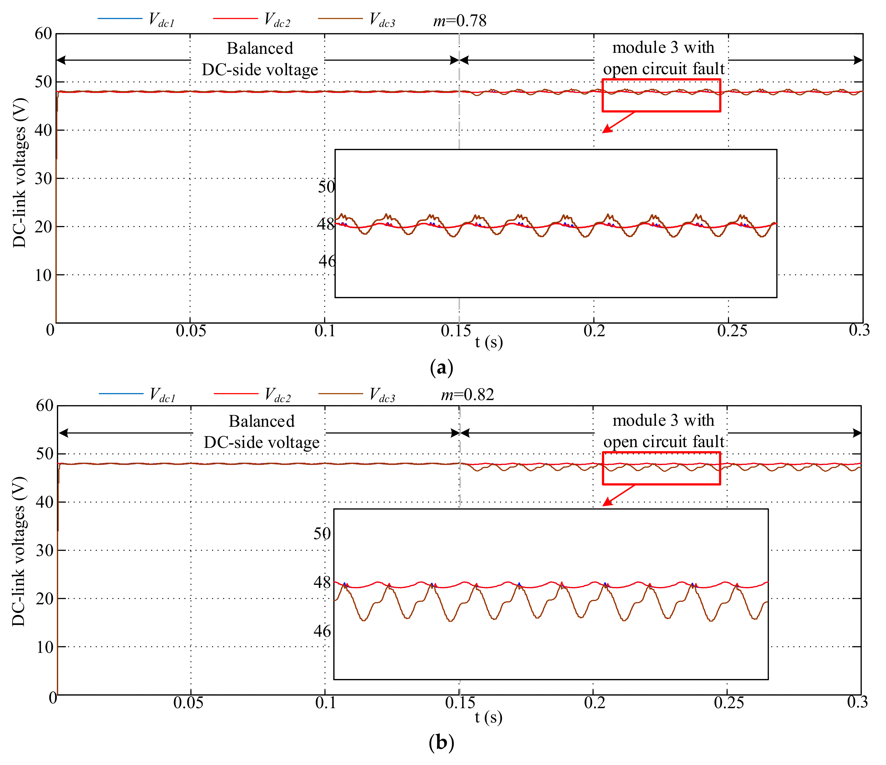
- An experiment platform is established in this paper. The dynamic performance is illustrated when DC-side input develops an open-circuit fault and must be cut off. The DC-side voltage can be recovered even if the extreme imbalance occurs. The ripple of the DC-side voltage is improved with the decreasing of modulation index. Additionally, the 3LNPC-CC has an excellent dynamic performance.
- (a)
- The proposed SSM could balance the DC-link voltage of the DC-port fault module, while the modulation index is under 0.8. The voltage-balancing ability is fairly high-level among voltage-balancing strategies;
- (b)
- The proposed SSM is able to find a proper switch-state path for voltage balancing that is suitable for the voltage balancing strategy. In addition, the proper switch-state path ensures the minimum switch-state changes and minimum frequency;
- (c)
- The proposed SSM takes the advantages from the smooth modulation and SPM by using a calculated table—not only for finding the proper switch state, but also for avoiding complex calculations while the 3LNPC-CC is working.
Author Contributions
Funding
Acknowledgments
Conflicts of Interest
References
- Ronanki, D.; Singh, S.; Williamson, S. Comprehensive Topological Overview of Rolling Stock Architectures and Recent Trends in Electric Railway Traction Systems. IEEE Trans. Transp. Electron. 2017, 3, 724–738. [Google Scholar] [CrossRef]
- Chung, Y.; Lee, C.; Kim, D.; Kang, H.; Park, Y.; Yoon, Y. Conceptual Design and Operating Characteristics of Multi-Resonance Antennas in the Wireless Power Charging System for Superconducting MAGLEV Train. IEEE Trans. Appl. Supercon. 2017, 27, 1–5. [Google Scholar] [CrossRef]
- Meng, T.; Song, Y.; Wang, Z.; Ben, H.; Li, C. Investigation and Implementation of an Input-Series Auxiliary Power Supply Scheme for High-Input-Voltage Low-Power Applications. IEEE Trans. Power Electron. 2018, 33, 437–447. [Google Scholar] [CrossRef]
- Yang, S.Y.; Bryant, A.; Mawby, P.; Xiang, D.W.; Ran, L.; Tavner, P. An industry-based survey of reliability in power electronic converters. In Proceedings of the IEEE Energy Conversion Congress and Exposition, San Jose, CA, USA, 20–24 September 2009. [Google Scholar] [CrossRef]
- An, F.; Song, W.; Yang, K.; Yang, S.; Ma, L. A Simple Power Estimation with Triple Phase-Shift Control for the Output Parallel DAB DC-DC Converters in Power Electronic Traction Transformer for Railway Locomotive Application. IEEE Trans. Transp. Electron. 2019, 5, 299–310. [Google Scholar] [CrossRef]
- Nabae, A.; Takahashi, I.; Akagi, H. A New Neutral-Point-Clamped PWM Inverter. IEEE Trans. Ind. Appl. 1981, 14, 518–522. [Google Scholar] [CrossRef]
- Kouro, S.; Malinowski, M.; Gopakumar, K.; Franquelo, J.; Wu, B.; Rodriguez, J. Recent Advances and Industrial Applications of Multilevel Converters. IEEE Trans. Ind. Electron. 2010, 57, 2553–2580. [Google Scholar] [CrossRef]
- Tu, P.; Yang, S.; Wang, P. Reliability and Cost-Based Redundancy Design for Modular Multilevel Converter. IEEE Trans. Ind. Electron. 2019, 66, 2333–2342. [Google Scholar] [CrossRef]
- Qi, C.; Chen, X.; Tu, P.; Wang, P. Cell-by-Cell-Based Finite-Control-Set Model Predictive Control for a Single-Phase Cascaded H-Bridge Rectifier. IEEE Trans. Power Electron. 2018, 33, 1654–1665. [Google Scholar] [CrossRef]
- He, X.; Lin, X.; Peng, X.; Han, P.; Shu, Z.; Gao, S. Control Strategy of Single-Phase Three Level Neutral Point Clamped Cascaded Rectifier. Energies 2017, 10. [Google Scholar] [CrossRef]
- She, X.; Huang, A.Q. Current sensorless power balance strategy for DC/DC converters in a cascaded multilevel converter based solid state transformer. IEEE Trans. Ind. Electron. 2014, 29, 17–22. [Google Scholar] [CrossRef]
- Peng, X.; He, X.; Han, P.; Lin, H.; Gao, S.; Shu, Z. Opposite Vector Based Phase Shift Carrier Space Vector Pulse Width Modulation for Extending the Voltage Balance Region in Single-Phase 3LNPC Cascaded Rectifier. IEEE Trans. Power Electron. 2016, 32, 7381–7393. [Google Scholar] [CrossRef]
- Peng, X.; He, X.; Han, P.; Guo, A.; Shu, Z.; Gao, S. Smooth Switching Technique for Voltage Balance Management Based on Three-Level Neutral Point Clamped Cascaded Rectifier. Energies 2016, 9, 803. [Google Scholar] [CrossRef]
- Peng, X.; He, X.; Han, P.; Lin, X.; Shu, Z.; Gao, S. Sequence Pulse Modulation for Voltage Balance in a Cascaded H-Bridge Rectifier. J. Power Electron. 2017, 17, 664–673. [Google Scholar] [CrossRef]
- Shu, Z.L.; He, X.Q.; Wang, Z.Y.; Qiu, D.Q.; Jing, Y.Z. Voltage Balancing Approaches for Diode-Clamped Multilevel Converters Using Auxiliary Capacitor-Based Circuits. IEEE Trans. Power Electron. 2012, 28, 2111–2124. [Google Scholar] [CrossRef]
- Shu, Z.L.; Zhu, H.F.; He, X.Q.; Ding, N.; Jing, Y.Z. One-inductor-based auxiliary circuit for dc-link capacitor voltage equalisation of diode-clamped multilevel converter. IET Power Electron. 2013, 6, 1339–1349. [Google Scholar] [CrossRef]
- Han, P.; He, X.; Zhao, Z.; Yu, H.; Wang, Y.; Peng, X.; Shu, Z. DC-Link Capacitor Voltage Balanced Modulation Strategy Based on Three Level Neutral Point Clamped Cascaded Rectifier. J. Power Electron. 2019, 19, 99–107. [Google Scholar] [CrossRef]
- Kwon, Y.A.; Kim, S.K. A High-Performance Strategy for Sensorless Induction Motor Drive Using Variable Link Voltage. IEEE Trans. Power Electron. 2007, 22, 329–332. [Google Scholar] [CrossRef]
- Tallam, R.M.; Naik, R.; Nondahl, T.A. A Carrier-Based Pwm Scheme for Neutral-Point Voltage Balancing in Three-Level Inverters. IEEE Trans. Ind. Appl. 2005, 41, 1734–1743. [Google Scholar] [CrossRef]
- Lin, H.; Shu, Z.; He, X.; Liu, M. N-D SVPWM with DC Voltage Balancing and Vector Smooth transition Algorithm for Cascaded Multilevel Converter. IEEE Trans. Ind. Electron. 2018, 65, 3837–3847. [Google Scholar] [CrossRef]
- He, X.; Yu, H.; Han, P.; Zhao, Z.; Peng, X.; Shu, Z.; Koh, L.; Wang, P. Fixed and Smooth-Switch-Sequence Modulation for Voltage Balancing Based on Single-Phase Three-Level Neutral Point Clamped Cascaded Rectifier. IEEE Trans. Ind. Appl. 2020. [Google Scholar] [CrossRef]
- Han, P.; He, X.; Ren, H.; Wang, Y.; Peng, X.; Shu, Z.; Gao, S.; Wang, Y.; Chen, Z. Fault Diagnosis and System Reconfiguration Strategy of a Single-Phase Three-Level Neutral-Point-Clamped Cascaded Inverter. IEEE Trans. Ind. Appl. 2020, 55, 3863–3876. [Google Scholar] [CrossRef]
- Busquets-Monge, S.; Griñó, R.; Nicolas-Apruzzese, J.; Bordonau, J. Decoupled DC-Link Capacitor Voltage Control of DC—AC Multilevel Multileg Converters. IEEE Trans. Ind. Electron. 2016, 63, 1344–1349. [Google Scholar] [CrossRef]
- Zhao, C.; Dujic, D.; Mester, A.; Steinke, J.K.; Weiss, M.; Lewdeni-Schmid, S.; Chaudhuri, T.; Stefanutti, P. Power Electronic Traction Transformer—Medium Voltage Prototype. IEEE Trans. Ind. Electron. 2013, 61, 3257–3268. [Google Scholar] [CrossRef]
- Dujic, D.; Kieferndorf, F.; Canales, F.; Drofenik, U. Power Electronic Traction Transformer Technology. In Proceedings of the IEEE 7th International Power Electronics and Motion Control Conference, Harbin, China, 2–5 June 2012. [Google Scholar] [CrossRef]


| M | S1st | S2nd | S3th |
|---|---|---|---|
| 6 | 2 | 2 | 2 |
| 5 | 2 | 2 | 1 |
| 4 | 2 | 2 | 0 |
| 3 | 2 | 2 | −1 |
| 2 | 2 | 2 | −2 |
| 1 | 1 | 1 | −1 |
| 0 | 0 | 0 | 0 |
| −1 | −1 | −1 | 1 |
| −2 | −2 | −2 | 2 |
| −3 | −2 | −2 | 1 |
| −4 | −2 | −2 | 0 |
| −5 | −2 | −2 | −1 |
| −6 | −2 | −2 | −2 |
| Parameter Name | Value |
|---|---|
| Number of the modules | 3 |
| DC-side voltage of each module | 48 V |
| Modulation index | 0.8 |
| Carrier wave frequency | 2 kHz |
| Switches | IGBT |
| Filter inductance | 1 mH |
| Filter capacitor | 10 μF |
| DC-side capacitor | 470 μF |
| Load | 50 Ω |
| Parameter Name | Value |
|---|---|
| Number of the cascade module | 3 |
| DC-side voltage | 48 V |
| Output voltage | 85 V |
| Controller (FPGA) | EP4CE10F17C8 N |
| Switch (IGBT) | FGA25N120ANTD |
| DC-side capacitance | 470 µF |
| Filter inductance | 1 mH |
| Filter capacitance | 10 µF |
| Load | 50 Ω |
| Carrier wave frequency | 2 kHz |
© 2020 by the authors. Licensee MDPI, Basel, Switzerland. This article is an open access article distributed under the terms and conditions of the Creative Commons Attribution (CC BY) license (http://creativecommons.org/licenses/by/4.0/).
Share and Cite
Yu, L.; Peng, X.; Zhou, C.; Gao, S. Voltage-Balancing Strategy for Three-Level Neutral-Point-Clamped Cascade Converter under Sequence Smooth Modulation. Energies 2020, 13, 4969. https://doi.org/10.3390/en13184969
Yu L, Peng X, Zhou C, Gao S. Voltage-Balancing Strategy for Three-Level Neutral-Point-Clamped Cascade Converter under Sequence Smooth Modulation. Energies. 2020; 13(18):4969. https://doi.org/10.3390/en13184969
Chicago/Turabian StyleYu, Le, Xu Peng, Chao Zhou, and Shibin Gao. 2020. "Voltage-Balancing Strategy for Three-Level Neutral-Point-Clamped Cascade Converter under Sequence Smooth Modulation" Energies 13, no. 18: 4969. https://doi.org/10.3390/en13184969
APA StyleYu, L., Peng, X., Zhou, C., & Gao, S. (2020). Voltage-Balancing Strategy for Three-Level Neutral-Point-Clamped Cascade Converter under Sequence Smooth Modulation. Energies, 13(18), 4969. https://doi.org/10.3390/en13184969