Abstract
Polysilane-inserted CH3NH3PbI3 perovskite photovoltaic devices combined with potassium and formamidinium iodides were fabricated and characterized. Decaphenylcyclopentasilane layers were inserted at the perovskite/hole transport interface and annealed across a temperature range of 180–220 °C. These polysilane-coated cells prevented PbI2 formation, and the conversion efficiencies were improved over extended periods of time.
1. Introduction
Although the most commonly used solar cells are currently silicon-based, these silicon devices have a complicated fabrication process, and the silicon semiconductor has an indirect transition band structure. Since recently developed CH3NH3PbI3 (MAPbI3)-based perovskite compounds have demonstrated numerous advantages, such as direct bandgaps, easy fabrication process, and high conversion efficiencies [1,2,3,4], these compounds are considered as major candidates for next-generation solar cell materials. However, lead halide compounds are typically unstable in air; thus, the stability of the corresponding perovskite photovoltaic devices should be improved for inclusion in the actual cell module [5,6]. The instability of the perovskite photovoltaic devices results from the migration of CH3NH3 (MA) and reactivity with H2O [7,8].
To improve the stability of the perovskite photovoltaic devices, polymeric materials have been investigated [9,10,11,12,13,14]. For instance, poly(methyl methacrylate) and poly(propylene carbonate) have been used to protect the perovskite layer from oxygen and moisture [15,16] and to enhance stability. Both polymeric materials formed cross-linked networks comprising perovskite grains, which suppressed defects. Furthermore, the stability was also influenced by hole transport layers (HTLs) [17]. In practice, 2,2′,7,7′-tetrakis(N,N-di-p-methoxyphenylamine)-9,9′-spirobifluorene (spiro-OMeTAD) is widely applied as a HTL for perovskite photovoltaic devices; however, this material is expensive, and the electronic properties degrade at elevated air temperatures. Alternative hole transport materials have been reported [18,19], and polysilane derivatives have also been investigated [20].
Polysilane derivatives exhibit two important advantages. The first relates to polysilanes being p-type semiconductors that facilitate hole transfer and rectification at the pn junction [20]. The second derives from polysilanes having high stabilities at elevated temperatures and therefore expected to act as a protective layer across the perovskite surface. Additionally, polysilanes have been applied to perovskite solar cells [21], and the photovoltaic properties were improved, especially by adding decaphenylcyclopentasilane (DPPS) [22,23,24]. However, the previously reported perovskite layers were a standard MAPbI3 compound, so further studies focusing on doped MAPbI3 compounds [25,26,27] are required to further elucidate the applicability of DPPS for perovskite solar cells.
Another method to improve the stability of perovskite solar cells is elemental or molecular doping of the perovskite crystals. The general formula of perovskite compounds is ABX3, where A and B are cations and X is an anion. The perovskite crystal with a cubic system has the B cations in sixfold coordination, surrounded by an octahedron of X anions and the A cation in octahedral coordination. The perovskite crystal of CH3NH3PbI3 is constructed with a Pb2+ cation at the B-site, I- anion at the X-site, and CH3NH3+ cation at the A-site. To estimate and predict the structural stabilities of the perovskite compounds, indicators called tolerance factors (t) have been calculated and used [27,28,29,30]. The tolerance factor is calculated as follows:
where rA, rB, and rX are the ionic radii of the A, B, and X ions. When t is close to 1, the perovskite structure is expected to be more structurally stable, although the ionic properties are not considered. The t-factor of MAPbI3 is calculated to be 0.912 [27], and this indicates MAPbI3 may be slightly unstable. To increase the t-factor and reduce the migration of MA, formamidinium (FA: CH3(NH2)2) with a larger ionic radius (2.53 Å) than MA (2.17 Å) was doped at the MA site, and the stabilities of the perovskite solar cells were improved by FA addition [31,32,33]. Studies on devices with ethylammonium (EA: CH3CH2NH3) [34,35] or guanidinium (GA: C(NH2)3) [36,37] addition to perovskites have also been reported. EA and GA have larger ionic radii (2.74 and 2.78 Å) than MA, and the addition of EA or GA can be expected to improve the structural stability from the viewpoint of the tolerance factors [27] and structural calculations [38,39]. It was reported that the crystallinity and stabilities of the perovskite crystals with EA were higher than those of ordinary MAPbI3 [40]. Then, EA or GA addition to the perovskite compounds provided surface coatings with fewer defects, highly (100)-oriented crystals, and improved stability of the devices [34,35,36,37]. However, it should be noted that excessive addition of EA leads to phase separation, a decrease in crystallinity, and precipitation of PbI2 as an impurity [41].
Since the above MA, FA, EA, and GA are molecules, they may affect the stabilities of the perovskite crystals. Therefore, substitution of alkali metal elements such as cesium (Cs), rubidium (Rb), potassium (K), and sodium (Na) might be effective in avoiding the migration and desorption of A-site elements in the perovskite crystals. It is also expected that the semiconductor characteristics of the perovskite crystals can be controlled by alkali element doping. Effects of Na and K doping to MAPbI3 crystals on the electronic structures were investigated by first-principles calculation [42]. Partial substitution of MA with Na or K generated electronic orbitals of Na or K above the conduction band, which would facilitate charge transfer from the alkali metals to the conduction band. This may then accelerate carrier diffusion related to the photovoltaic performances. Conversion efficiencies and stabilities were reported to be improved by adding Cs+ and Rb+ to perovskite precursor solutions, which increased grain sizes and reduced defect densities [43,44,45,46]. Conversion efficiencies were also improved by using K, which offers a lower cost than Rb and Cs. A calculated t-factor of K doping alone to MAPbI3 indicates that the structural stability of perovskite compounds was reduced [27], and other cations with larger cationic radii, such as FA and EA, may be necessary to form more stable perovskite structures.
Herein, the focus is to investigate the photovoltaic properties and stabilities of DPPS-inserted MAPbI3 perovskite solar cells doped with potassium (K) and formamidinium (FA), which are denoted as MA(FA, K)PbI3. Previously, co-addition of K and FA was reported to be effective for enhancing the photovoltaic properties [47,48,49,50,51]. In the present work, the MA(FA,K)PbI3 perovskite compounds, prepared at temperatures in the range of 180–220 °C in ambient air, were evaluated in terms of the photovoltaic properties and stability. The effects of annealing temperatures and polysilane addition on the microstructures and photovoltaic properties of the MA(FA, K)PbI3 perovskite solar cells were investigated using current density voltage (J-V) characteristics and X-ray diffraction (XRD).
2. Materials and Methods
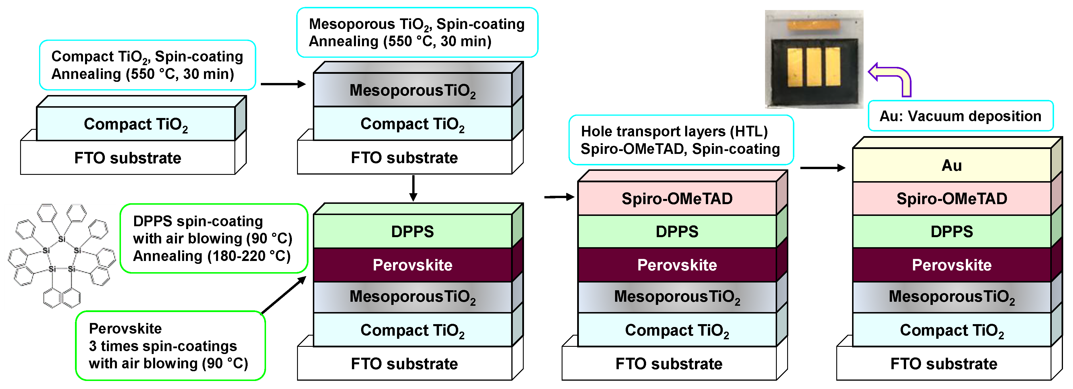
A fabrication process of the present solar cell devices is schematically illustrated in Figure 1. The fabrication conditions were ~27 °C temperature and ~40% humidity in ambient air [52,53]. F-doped tin oxide (FTO, Nippon Sheet Glass Company, Tokyo, Japan, ~10 Ω/□) substrates were cleaned by methanol and acetone in an ultrasonic bath and an ultraviolet ozone cleaner (Asumi Giken, Tokyo, Japan, ASM401N) [26,54]. Next, 0.15 and 0.30 M precursor solutions of TiO2 compact layers were prepared from 1-butanol (Wako Pure Chemical Industries, Osaka, Japan) and titanium diisopropoxide bis(acetylacetonate) (Sigma Aldrich, Tokyo, Japan). These precursor solutions of compact TiO2 were spin-coated on the FTO substrate at 3000 rpm for 30 s, and the substrates were annealed at 125 °C for 5 min. To form a uniform compact TiO2 layer, the 0.30 M precursor solution was spin-coated twice. Then, the FTO substrate was annealed at 550 °C for 30 min to form the compact TiO2 layer. After that, a TiO2 paste (precursor solution for mesoporous TiO2) was spin-coated on the compact TiO2 layer at 5000 rpm for 30 s. This TiO2 paste was prepared by mixing distilled water (0.5 mL), poly(ethylene glycol) PEG-20000 (Nacalai Tesque, Kyoto, Japan, PEG #20000, 20 mg), and TiO2 powder (Aerosil, Tokyo, Japan, P-25, 200 mg). This solution was further mixed with the surfactant Triton X-100 (Sigma Aldrich, 10 μL) and acetylacetone (Wako Pure Chemical Industries, 20 μL) for 30 min, and it was left untouched for 24 h to remove bubbles in the solution [53]. To form the mesoporous TiO2 layer, the TiO2-coated substrates were annealed at 550 °C for 30 min.
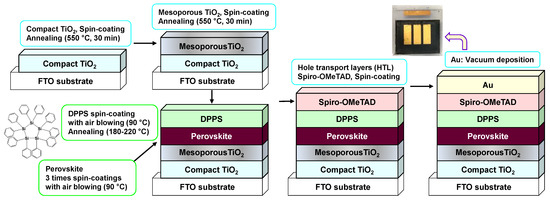
Figure 1.
Schematic illustration detailing the processes adopted to fabricate the perovskite photovoltaic devices and a photograph of the device.
The perovskite compounds were prepared by mixing N,N-dimethylformamide (DMF; Sigma Aldrich) solutions of KI (Wako Pure Chemical Industries), HC(NH2)2I (Tokyo Chemical Industry, Tokyo, Japan), CH3NH3I (Tokyo Chemical Industry), and PbCl2 (Sigma Aldrich) at 60 °C for 1 day. The basic precursor of MAPbI3 was prepared with molar concentrations of PbCl2 and MAI of 0.8 and 2.4 M, respectively [53,55], and MA0.64FA0.31K0.05PbI3 and MA0.48FA0.47K0.05PbI3 precursors were prepared by adding FAI and KI to control the desired molar ratio. As the FA composition increased, the tolerance factor (t-factor) increased toward 1 [27], which indicated the crystal distortion in the perovskite structure could be reduced by FA addition. Perovskite precursor solutions were spin-coated on the mesoporous TiO2 layer three times. For the first spin-coating, the perovskite solutions were spin-coated at 2000 rpm for 60 s. During the second and third spin-coatings, a hot air-blowing method was applied [27]. Temperatures of the cells during the air-blowing were set at 90 °C. A polysilane solution was prepared by mixing chlorobenzene (Fujifilm Wako Pure Chemical Corporation, 0.5 mL) with DPPS (Osaka Gas Chemicals, Osaka, Japan, OGSOL SI-30-10, 10 mg). During the last 15 s of the third spin-coating of the perovskite precursor solutions, the DPPS polysilane solution was also spin-coated on the perovskite layer [24]. The prepared cells were then annealed at 180 and 200 °C for 10 min, and at 220 °C for 5 min in ambient air.
Hole transporting layers were spin-coated at 4000 rpm for 30 s. A precursor solution of the hole transporting layer was prepared by mixing chlorobenzene (0.5 mL; Wako Pure Chemical Industries) and spiro-OMeTAD (Sigma Aldrich 36.1 mg) for 24 h. An acetonitrile (Nacalai Tesque, 0.5 mL) solution of lithium bis(trifluoromethylsulfonyl)imide (Tokyo Chemical Industry, 260 mg) was similarly prepared by 24 h stirring. This lithium bis(trifluoromethylsulfonyl)imide solution (8.8 µL) was added to the spiro-OMeTAD solution mixed with 4-tert-butylpyridine (Sigma Aldrich, 14.4 µL) and stirred at 70 °C for 30 min. Lastly, top-electrodes of gold (Au) were formed by a vacuum evaporating system (Sanyu Electron, Tokyo, Japan, SVC-700TMSG). All the fabricated devices were stored at 22 °C and ~30% humidity in ambient air.
The current density voltage characteristics (Keysight, Santa Rosa, CA, USA, B2901A) of the fabricated devices were measured under a solar simulating light source (San-ei Electric, Osaka, Japan, XES-301S) operated at 100 mW cm−2 (air mass 1.5). The exposed area of the photovoltaic devices was 0.080 cm2. An X-ray diffractometer (Bruker, Billerica, MA, USA, D2 PHASER) was used for microstructural analysis of the perovskite crystals.
3. Results
Conversion efficiencies and other parameters of the present perovskite solar cells are summarized in Table 1, where η is the photoconversion efficiency, ηave is the average conversion efficiency of the three devices, VOC is the open-circuit voltage, JSC is the short-circuit current density, Rsh is the shunt resistance, RS is the series resistance, and FF is the fill factor. For the as-prepared devices, those annealed at 200 °C exhibited the highest photoconversion efficiencies of 10.99% and 6.20% for MA0.64FA0.31K0.05PbI3 and MA0.48FA0.47K0.05PbI3, respectively.

Table 1.
Measured photovoltaic parameters of the present perovskite solar cells.
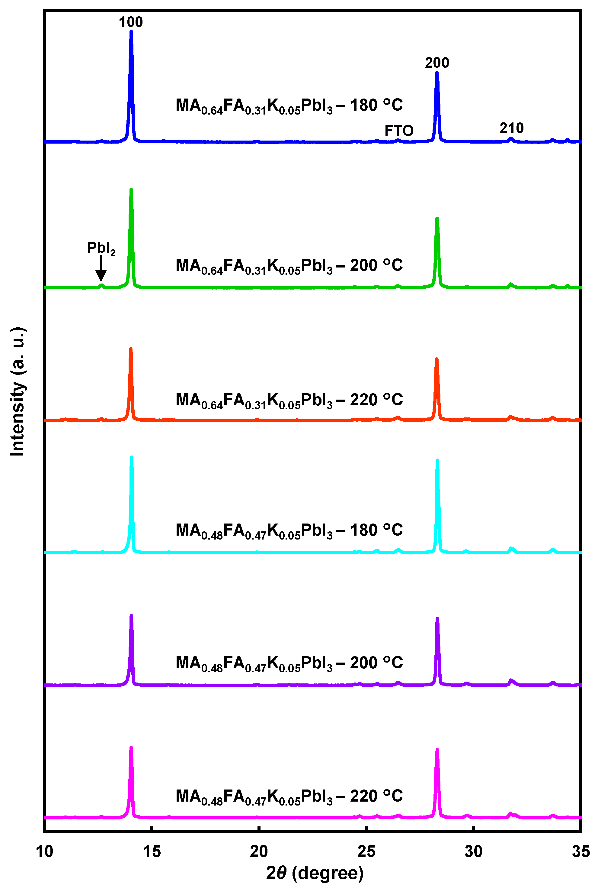
XRD patterns of the perovskite solar cells are shown in Figure 2. In all devices, highly (100)-oriented crystals of the perovskite compounds were observed, which were formed by the hot air-blowing method [27]. All devices presented few peaks corresponding to PbI2, which indicated the effectiveness of the DPPS layer against high-temperature annealing at ~200 °C. Although peaks of lesser intensities, assigned to PbI2, were observed for the MA0.64FA0.31K0.05PbI3 devices, especially when annealed at 200 °C, almost no PbI2 formation was observed for the MA0.48FA0.47K0.05PbI3 devices, even after annealing at 220 °C. The FA-rich composition contributed to the stability of the cubic perovskite and suppressed PbI2 formation.
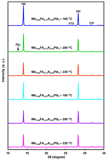
Figure 2.
Measured XRD patterns of the present perovskite solar cells.
The lattice constants of the perovskites increased as a function of temperature, as shown in Table 2. Additionally, the lattice constant should also increase as FA composition increases because of the larger FA ionic size compared with MA. However, the lattice constant of FA-rich MA0.48FA0.47K0.05PbI3 was smaller than that of MA0.64FA0.31K0.05PbI3, which is suggested to be related with K occupancy at the MA site.

Table 2.
Measured lattice constants and crystallite sizes of the perovskite compounds.
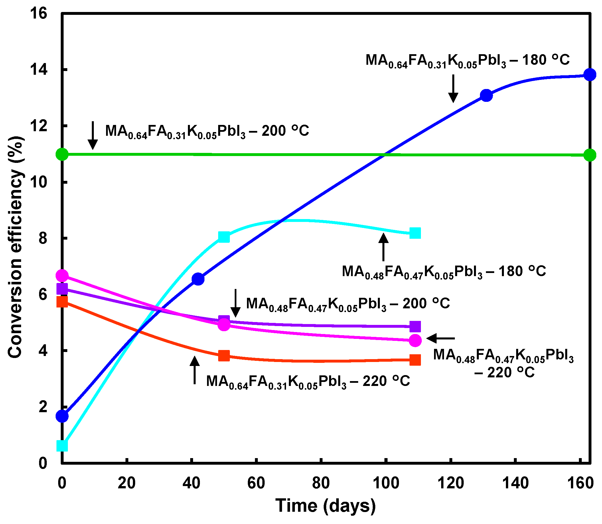
Figure 3 shows conversion efficiency changes of the perovskite photovoltaic devices. For the as-prepared devices, those annealed at 200 °C showed the highest conversion efficiencies and were almost identical to the conversion efficiencies after 163 days. Conversely, the conversion efficiency of the MA0.48FA0.47K0.05PbI3 device, prepared at 180 °C, improved from 0.613% to 8.18% after 109 days, as shown in Figure 3. For the devices annealed at 220 °C, the conversion efficiencies decreased after 50 days.

Figure 3.
Changes of photoconversion efficiencies of the present perovskite photovoltaic devices.
Changes to the J-V characteristics of the MA0.64FA0.31K0.05PbI3 device, prepared at 180 °C, are shown in Figure 4. For the as-prepared device, the highest conversion efficiency was observed at 1.67%, as shown in Table 1. After 42 days, VOC and JSC were improved. Furthermore, FF also improved after 131 days. After 163 days, the photovoltaic properties of the MA0.64FA0.31K0.05PbI3 device were further enhanced, and the highest conversion efficiency of 13.82%, a VOC of 0.970 V, a JSC of 20.3 mA cm−2, and a FF of 0.700 were obtained, as shown in Figure 3 and Table 1.
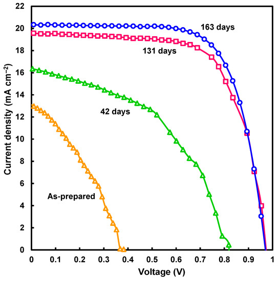
Figure 4.
Changes of current density voltage characteristics of the MA0.64FA0.31K0.05PbI3 device prepared at 180 °C for 10 min.
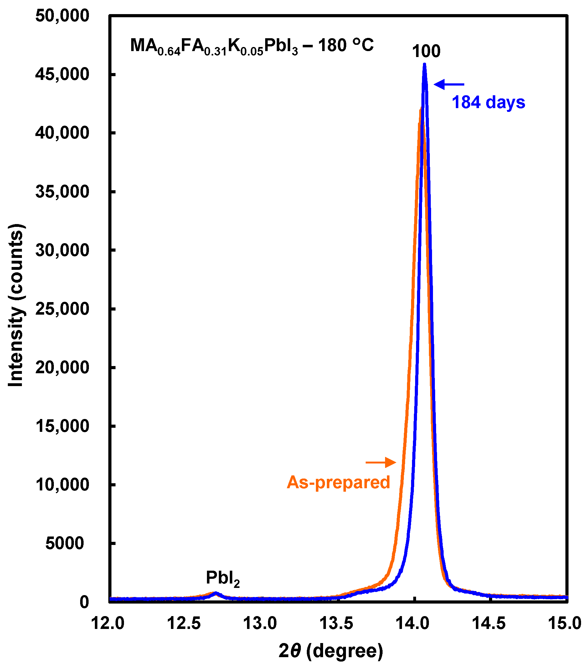
Microstructural changes of the MA0.64FA0.31K0.05PbI3 device annealed at 180 °C were investigated by XRD, as shown in Figure 5. Small PbI2 peaks were observed in both XRD patterns, and further PbI2 formation was suppressed, even after six months. Full-width at half maximum (FWHM) for the MA0.64FA0.31K0.05PbI3 device was reduced after six months, which indicated the crystallite size of the perovskite increased, as shown in Table 2. The XRD observations indicated the crystal growth of the perovskite compound, which led to a decrease in the grain boundary area and point defects and, hence, improvement in the photovoltaic performance. The lattice constant of the perovskite compound was observed to decrease slightly, as shown in Table 2, which relates to the desorption of a small amount of MA.

Figure 5.
Comparison of the XRD patterns of the MA0.64FA0.31K0.05PbI3 devices as a function of time, prepared at 180 °C for 10 min.
Conversion efficiencies of polysilane-inserted perovskite solar cells were improved in previous studies [22,24]. The MAPbI3 device annealed at 190 °C showed an efficiency of 11.57%, which increased to 13.36% after four weeks, and the increases were within 2%. On the other hand, the conversion efficiency of the present solar cell prepared at 180 °C increased from 1.67% to 13.82%, with an increase of efficiency over 12%. To describe this abnormal increase, three mechanisms for the rise in conversion efficiencies of the MA0.64FA0.31K0.05PbI3 device, prepared at 180 °C, can be considered.
The first is crystallization of the amorphous phase into the perovskite crystal at room temperature. During the spin-coating of DPPS, a mixed composite layer comprising amorphous perovskite and DPPS, having a dense interface, was formed during room temperature aging. In addition, K might compensate MA defects during the aging. Since DPPS also functions as a HTL [20], holes are able to smoothly transport at the perovskite/DPPS/spiro-OMeTAD interface. Other annealing methods, such as laser-annealing and flash light annealing, have been reported [56,57] and may also be effective for the crystallization of the perovskite compounds.
The second mechanism relates to the formation of a small amount of PbI2 at the perovskite surface immediately under the DPPS and spiro-OMeTAD layers. A small decrease of the MA0.64FA0.31K0.05PbI3 lattice constant implies desorption of MA, with PbI2 suggested to be formed at the surface of the perovskite crystals. PbI2 is a p-type semiconductor with a bandgap energy of ~2.5 eV and functions as an electron blocking layer [58,59]. Thereafter, FF and conversion efficiency increase.
The third mechanism relates to the interface at the perovskite/spiro-OMeTAD. Since the VOC and Rsh had a fairly large increase, the interface would also act as an n-i-p junction instead of the simple back-surface field effect in Si solar cells. The J-V curve as a function of time in Figure 4 demonstrated a typical shape change as the Rsh increased. Slow annealing at lower temperatures may provide more uniform and dense perovskite layers.
4. Conclusions
In summary, the influences of DPPS layer insertion between the MA(FA, K)PbI3 perovskite layer and HTL on the microstructures and photovoltaic properties were examined. For the as-prepared devices, those annealed at 200 °C exhibited the highest photoconversion efficiencies, whereas the conversion efficiencies of the devices annealed at 220 °C decreased after 50 days. Conversely, the photovoltaic properties of the MA0.64FA0.31K0.05PbI3 device annealed at 180 °C were improved after 163 days, and the device provided the highest photoconversion efficiency of 13.82%. Microstructures of the perovskite compounds were investigated by XRD, which indicated suppression of PbI2 formation for the DPPS-added device formed at 180 °C, even after six months. Increased crystallite sizes of the MA0.64FA0.31K0.05PbI3 perovskite promoted a decrease of the grain boundary area and point defects, which reduced the current leakage and improved the photovoltaic performance. The present results indicate that polysilane insertion and high-temperature annealing are effective for the improvement of the conversion efficiencies of perovskite photovoltaic devices.
Author Contributions
Conceptualization, T.O. and S.K.; Methodology, T.O., S.K., M.T., and A.S.; Formal Analysis, T.O. and S.K.; Investigation, S.K.; Resources, M.O., S.M., S.F., and T.T.; Data Curation, T.O. and S.K.; Writing—Original Draft Preparation, T.O.; Writing—Review & Editing, S.K., M.T., A.S., M.O., S.M., S.F., and T.T.; Project Administration, T.O.; Funding Acquisition, T.O. All authors have read and agreed to the published version of the manuscript.
Funding
A part of the present study was supported by the Japan Science and Technology Agency (JST).
Conflicts of Interest
The authors declare no conflict of interest.
References
- Li, N.; Zhu, Z.; Chueh, C.C.; Liu, H.; Peng, B.; Petrone, A.; Li, X.; Wang, L.; Jen, A.K.Y. Mixed cation FAxPEA1−xPbI3 with enhanced phase and ambient stability toward high-performance perovskite solar cells. Adv. Energy Mater. 2017, 7, 1601307. [Google Scholar] [CrossRef]
- Gedamu, D.; Asuo, I.M.; Benetti, D.; Basti, M.; Ka, I.; Cloutier, S.G.; Rosei, F.; Nechache, R. Solvent-antisolvent ambient processed large grain size perovskite thin films for high-performance solar cells. Sci. Rep. 2018, 8, 12885. [Google Scholar] [CrossRef] [PubMed]
- Miyasaka, T.; Kulkarni, A.; Kim, G.M.; Öz, S.; Jena, A.K. Perovskite solar cells: Can we go organic-free, lead-free, and dopant-free? Adv. Energy Mater. 2020, 10, 1902500. [Google Scholar] [CrossRef]
- Tong, J.; Song, Z.; Kim, D.M.; Chen, X.; Chen, C.; Palmstrom, A.F.; Ndione, P.F.; Reese, M.O.; Dunfield, S.P.; Reid, O.G.; et al. Carrier lifetimes of >1 μs in Sn-Pb perovskites enable efficient all-perovskite tandem solar cells. Science 2019, 364, 475–479. [Google Scholar] [CrossRef] [PubMed]
- Zhang, X.; Yin, J.; Nie, Z.; Zhang, Q.; Sui, N.; Chen, B.; Zhang, Y.; Qu, K.; Zhao, J.; Zhou, H. Lead-free and amorphous organic–inorganic hybrid materials for photovoltaic applications: Mesoscopic CH3NH3MnI3/TiO2 heterojunction. RSC Adv. 2017, 7, 37419–37425. [Google Scholar] [CrossRef]
- Dong, H.; Wu, Z.; Xi, J.; Xu, X.; Zuo, L.; Lei, T.; Zhao, X.; Zhang, L.; Hou, X. Pseudohalide-induced recrystallization engineering for CH3NH3PbI3 film and its application in highly efficient inverted planar heterojunction perovskite solar cells. Adv. Funct. Mater. 2017, 28, 1704836. [Google Scholar] [CrossRef]
- Dunfield, S.P.; Bliss, L.; Zhang, F.; Luther, J.M.; Zhu, K.; Van Hest, M.F.A.M.; Reese, M.O.; Berry, J.J. From defects to degradation: A mechanistic understanding of degradation in perovskite solar cell devices and modules. Adv. Energy Mater. 2020, 10, 1904054. [Google Scholar] [CrossRef]
- Lee, J.W.; Kim, S.G.; Yang, J.M.; Yang, Y.; Park, N.G. Verification and mitigation of ion migration in perovskite solar cells. APL Mater. 2019, 7, 041111. [Google Scholar] [CrossRef]
- Chen, H.W.; Huang, T.Y.; Chang, T.H.; Sanehira, Y.; Kung, C.W.; Chu, C.W.; Ikegami, M.; Miyasaka, T.; Ho, K.C. Efficiency enhancement of hybrid perovskite solar cells with MEH-PPV hole-transporting layers. Sci. Rep. 2016, 6, 34319. [Google Scholar] [CrossRef]
- Bi, D.; Yi, C.; Luo, J.; Decoppet, J.D.; Zhang, F.; Zakeeruddin, S.M.; Li, X.; Hagfeldt, A.; Gratzel, M. Polymer-templated nucleation and crystal growth of perovskite films for solar cells with efficiency greater than 21%. Nat. Energy 2016, 1, 16142. [Google Scholar] [CrossRef]
- Zhang, S.; Lu, Y.; Lin, B.; Zhu, Y.; Zhang, K.; Yuan, N.Y.; Ding, J.N.; Fang, B. PVDF-HFP additive for visible-light-semitransparent perovskite films yielding enhanced photovoltaic performance. Sol. Energy Mater. Sol. Cells 2017, 170, 178–186. [Google Scholar] [CrossRef]
- Zuo, L.; Guo, H.; deQuilettes, D.W.; Jariwala Marco, S.N.D.; Dong, S.; De Block, R.; Ginger, D.S.; Dunn, B.; Wang, M. Polymer-modified halide perovskite films for efficient and stable planar heterojunction solar cells. Sci. Adv. 2017, 3, e1700106. [Google Scholar] [CrossRef] [PubMed]
- Zhang, H.; Shi, J.; Zhu, L.; Luo, Y.; Li, D.; Wu, H.; Meng, Q. Polystyrene stabilized perovskite component, grain and microstructure for improved efficiency and stability of planar solar cells. Nano Energy 2018, 43, 383–392. [Google Scholar] [CrossRef]
- Chen, Z.; Dong, Q.; Liu, Y.; Bao, C.; Fang, Y.; Lin, Y.; Tang, S.; Wang, Q.; Xiao, X.; Bai, Y.; et al. Thin single crystal perovskite solar cells to harvest below-bandgap light absorption. Nat. Commun. 2017, 8, 1890. [Google Scholar] [CrossRef]
- Wang, F.; Shimazaki, A.; Yang, F.; Kanahashi, K.; Matsuki, K.; Miyauchi, Y.; Takenobu, T.; Wakamiya, A.; Murata, Y.; Matsuda, K. Highly efficient and stable perovskite solar cells by interfacial engineering using solution-processed polymer layer. J. Phys. Chem. C 2017, 121, 1562–1568. [Google Scholar] [CrossRef]
- Han, T.H.; Lee, J.W.; Choi, C.; Tan, S.; Lee, C.; Zhao, Y.; Dai, Z.; Marco, N.D.; Lee, S.J.; Bae, S.H.; et al. Perovskite-polymer composite cross-linker approach for highly-stable and efficient perovskite solar cells. Nat. Commun. 2019, 10, 520. [Google Scholar] [CrossRef]
- Kim, G.W.; Choi, H.; Kim, M.; Lee, J.; Son, S.Y.; Park, T. Hole transport materials in conventional structural (n–i–p) perovskite solar cells: From past to the future. Adv. Energy Mater. 2020, 10, 1903403. [Google Scholar] [CrossRef]
- Tavakoli, M.M.; Tavakoli, R.; Prochowicz, D.; Yadav, P.; Saliba, M. Surface modification of a hole transporting layer for an efficient perovskite solar cell with an enhanced fill factor and stability. Mol. Syst. Des. Eng. 2018, 3, 717–722. [Google Scholar] [CrossRef]
- Mabrouk, S.; Zhang, M.; Wang, Z.; Liang, M.; Bahrami, B.; Wu, Y.; Wu, J.; Qiao, Q.; Yang, S. Dithieno[3,2-b:2′,3′-d]pyrrole-based hole transport materials for perovskite solar cells with efficiencies over 18%. J. Mater. Chem. A 2018, 6, 7950–7958. [Google Scholar] [CrossRef]
- Oku, T.; Nakagawa, J.; Iwase, M.; Kawashima, A.; Yoshida, K.; Suzuki, A.; Akiyama, T.; Tokumitsu, K.; Yamada, M.; Nakamura, M. Microstructures and photovoltaic properties of polysilane-based solar cells. Jpn. J. Appl. Phys. 2013, 52, 04CR07. [Google Scholar] [CrossRef]
- Shirahata, Y.; Yamamoto, Y.; Suzuki, A.; Oku, T.; Fukunishi, S.; Kohno, K. Effects of polysilane-doped spiro-OMeTAD hole transport layers on photovoltaic properties. Phys. Status Solidi A 2017, 214, 1600591. [Google Scholar] [CrossRef]
- Taguchi, M.; Suzuki, A.; Oku, T.; Fukunishi, S.; Minami, S.; Okita, M. Effects of decaphenylcyclopentasilane addition on photovoltaic properties of perovskite solar cells. Coatings 2018, 8, 461. [Google Scholar] [CrossRef]
- Oku, T.; Nomura, J.; Suzuki, A.; Tanaka, H.; Fukunishi, S.; Minami, S.; Tsukada, S. Fabrication and characterization of CH3NH3PbI3 perovskite solar cells added with polysilanes. Int. J. Photoenergy 2018, 8654963. [Google Scholar] [CrossRef]
- Taguchi, M.; Suzuki, A.; Oku, T.; Ueoka, N.; Minami, S.; Okita, M. Effects of annealing temperature on decaphenylcyclopentasilane-inserted CH3NH3PbI3 perovskite solar cells. Chem. Phys. Lett. 2019, 737, 136822. [Google Scholar] [CrossRef]
- Ueoka, N.; Oku, T.; Suzuki, A. Additive effects of alkali metals on Cu-modified CH3NH3PbI3-δClδ photovoltaic devices. RSC Adv. 2019, 9, 24231–24240. [Google Scholar] [CrossRef]
- Ueoka, N.; Oku, T. Effects of co-addition of sodium chloride and copper(II) bromide to mixed-cation mixed-halide perovskite photovoltaic devices. ACS Appl. Energy Mater. 2020, 3, 7272–7283. [Google Scholar] [CrossRef]
- Oku, T. Crystal structures of perovskite halide compounds used for solar cells. Rev. Adv. Mater. Sci. 2020, 59, 264–305. [Google Scholar] [CrossRef]
- Travis, W.; Glover, E.N.K.; Bronstein, H.; Scanlon, D.O.; Palgrave, R.G. On the application of the tolerance factor to inorganic and hybrid halide perovskites: A revised system. Chem. Sci. 2016, 7, 4548–4556. [Google Scholar] [CrossRef]
- Hoefler, S.F.; Trimmel, G.; Rath, T. Progress on lead-free metal halide perovskites for photovoltaic applications: A review. Monatsh. Chem. 2017, 148, 795–826. [Google Scholar] [CrossRef]
- Tanaka, H.; Oku, T.; Ueoka, N. Structural stabilities of organic–inorganic perovskite crystals. Jpn. J. Appl. Phys. 2018, 57, 08RE12. [Google Scholar] [CrossRef]
- Zhou, Y.; Yang, M.; Pang, S.; Zhu, K.; Padture, N.P. Exceptional morphology-preserving evolution of formamidinium lead triiodide perovskite thin films via organic-cation displacement. J. Am. Chem. Soc. 2016, 138, 5535–5538. [Google Scholar] [CrossRef] [PubMed]
- Hu, M.; Liu, L.; Mei, A.; Yang, Y.; Liu, T.; Han, H. Efficient hole conductor-free, fully printable mesoscopic perovskite solar cells with a broad light harvester NH2CH=NH2PbI3. J. Mater. Chem. A 2014, 2, 17115–17121. [Google Scholar] [CrossRef]
- Suzuki, A.; Kato, M.; Ueoka, N.; Oku, T. Additive effect of formamidinium chloride in methylammonium lead halide compound-based perovskite solar cells. J. Electron. Mater. 2019, 48, 3900–3907. [Google Scholar] [CrossRef]
- Wang, Y.; Zhang, T.; Li, G.; Xu, F.; Li, Y.; Yang, Y.; Zhao, Y. A mixed-cation lead iodide MA1−xEAxPbI3 absorber for perovskite solar cells. J. Energy Chem. 2018, 27, 215–218. [Google Scholar] [CrossRef]
- Nishi, K.; Oku, T.; Kishimoto, T.; Ueoka, N.; Suzuki, A. Photovoltaic characteristics of CH3NH3PbI3 perovskite solar cells added with ethylammonium bromide and formamidinium iodide. Coatings 2020, 10, 410. [Google Scholar] [CrossRef]
- Jodlowski, A.D.; Roldán-Carmona, C.; Grancini, G.; Salado, M.; Ralaiarisoa, M.; Ahmad, S.; Koch, N.; Camacho, L.; Miguel, G.; Nazeeruddin, M. Large guanidinium cation mixed with methylammonium in lead iodide perovskites for 19% efficient solar cells. Nat. Energy 2017, 2, 972–979. [Google Scholar] [CrossRef]
- Kishimoto, T.; Suzuki, A.; Ueoka, N.; Oku, T. Effects of guanidinium addition to CH3NH3PbI3−xClx perovskite photovoltaic devices. J. Ceram. Soc. Jpn. 2019, 127, 491–497. [Google Scholar] [CrossRef]
- Liu, D.; Li, Q.; Wu, K. Ethylammonium as an alternative cation for efficient perovskite solar cells from first-principles calculations. RSC Adv. 2019, 9, 7356–7361. [Google Scholar] [CrossRef]
- Arkan, F.; Mohammad, I. Computational modeling of the photovoltaic activities in EABX3 (EA = ethylammonium, B = Pb, Sn, Ge, X = Cl, Br, I) perovskite solar cells. Comput. Mater. Sci. 2018, 152, 324–330. [Google Scholar] [CrossRef]
- Zhang, F.; Cong, J.; Li, Y.; Bergstrand, J.; Liu, H.; Cai, B.; Hajian, A.; Yao, Z.; Wang, L.; Hao, Y.; et al. A facile route to grain morphology controllable perovskite thin films towards highly efficient perovskite solar cells. Nano Energy 2018, 53, 405–414. [Google Scholar] [CrossRef]
- Ueoka, N.; Oku, T.; Tanaka, H.; Suzuki, A.; Sakamoto, H.; Yamada, M.; Minami, S.; Miyauchi, S.; Tsukada, S. Effects of PbI2 addition and TiO2 electron transport layers for perovskite solar cells. Jpn. J. Appl. Phys. 2018, 57, 08RE05. [Google Scholar] [CrossRef]
- Suzuki, A.; Miyamoto, Y.; Oku, T. Electronic structures, spectroscopic properties, and thermodynamic characterization of sodium or potassium-incorporated CH3NH3PbI3 by first principles calculation. J. Mater. Sci. 2020, 55, 9728–9738. [Google Scholar] [CrossRef]
- Bush, K.A.; Frohna, K.; Prasanna, R.; Beal, R.E.; Leijtens, T.; Swifter, S.A.; McGehee, M.D. Compositional engineering for efficient wide band gap perovskites with improved stability to photoinduced phase segregation. ACS Energy Lett. 2018, 3, 428–435. [Google Scholar] [CrossRef]
- Liu, C.; Kong, W.; Li, W.; Chen, H.; Li, D.; Wang, W.; Xu, B.; Cheng, C.; Jen, A.K.Y. Enhanced stability and photovoltage for inverted perovskite solar cells via precursor engineering. J. Mater. Chem. A 2019, 7, 15880–15886. [Google Scholar] [CrossRef]
- Zhang, M.; Yun, J.S.; Ma, Q.; Zheng, J.; Lau, C.F.J.; Deng, X.; Kim, J.; Kim, D.; Seidel, J.; Green, M.A.; et al. High-efficiency rubidium-incorporated perovskite solar cells by gas quenching. ACS Energy Lett. 2017, 2, 438–444. [Google Scholar] [CrossRef]
- Turren-Cruz, S.H.; Saliba, M.; Mayer, M.T.; Juárez-Santiesteban, H.; Mathew, X.; Nienhaus, L.; Tress, W.; Erodici, M.P.; Sher, M.J.; Bawendi, M.G.; et al. Enhanced charge carrier mobility and lifetime suppress hysteresis and improve efficiency in planar perovskite solar cells. Energy Environ. Sci. 2018, 11, 78–86. [Google Scholar] [CrossRef]
- Zheng, F.; Chen, W.; Bu, T.; Ghiggino, K.P.; Huang, F.; Cheng, Y.; Tapping, P.; Kee, T.W.; Jia, B.; Wen, X. Triggering the passivation effect of potassium doping in mixed-cation mixed-halide perovskite by light illumination. Adv. Energy Mater. 2019, 9, 1901016. [Google Scholar] [CrossRef]
- Liu, X.; Zhang, Y.; Shi, L.; Liu, Z.; Huang, J.; Yun, J.S.; Zeng, Y.; Pu, A.; Sun, K.; Hameiri, Z.; et al. Exploring inorganic binary alkaline halide to passivate defects in low-temperature-processed planar-structure hybrid perovskite solar cells. Adv. Energy Mater. 2018, 8, 1800138. [Google Scholar] [CrossRef]
- Jalebi, M.A.; Garmaroudi, Z.A.; Pearson, A.J.; Divitini, G.; Cacovich, S.; Philippe, B.; Rensmo, H.; Ducati, C.; Friend, R.H.; Stranks, S.D. Potassium- and rubidium-passivated alloyed perovskite films: Optoelectronic properties and moisture stability. ACS Energy Lett. 2018, 3, 2671–2678. [Google Scholar] [CrossRef]
- Machiba, H.; Oku, T.; Kishimoto, T.; Ueoka, N.; Suzuki, A. Fabrication and evaluation of K-doped MA0.8FA0.1K0.1PbI3(Cl) perovskite solar cells. Chem. Phys. Lett. 2019, 730, 117–123. [Google Scholar] [CrossRef]
- Kandori, S.; Oku, T.; Nishi, K.; Kishimoto, T.; Ueoka, N.; Suzuki, A. Fabrication and characterization of potassium- and formamidinium-added perovskite solar cells. J. Ceram. Soc. Jpn. 2020, 128. in press. [Google Scholar]
- Oku, T.; Zushi, M.; Imanishi, Y.; Suzuki, A.; Suzuki, K. Microstructures and photovoltaic properties of perovskite-type CH3NH3PbI3 compounds. Appl. Phys. Express 2014, 7, 121601. [Google Scholar] [CrossRef]
- Oku, T.; Ohishi, Y.; Ueoka, N. Highly (100)-oriented CH3NH3PbI3(Cl) perovskite solar cells prepared with NH4Cl using an air blow method. RSC Adv. 2018, 8, 10389–10395. [Google Scholar] [CrossRef]
- Oku, T.; Ohishi, Y.; Suzuki, A.; Miyazawa, Y. Effects of NH4Cl addition to perovskite CH3NH3PbI3 photovoltaic devices. J. Ceram. Soc. Jpn. 2017, 125, 303–307. [Google Scholar] [CrossRef]
- Oku, T.; Ohishi, Y. Effects of annealing on CH3NH3PbI3(Cl) perovskite photovoltaic devices. J. Ceram. Soc. Jpn. 2018, 126, 56–60. [Google Scholar] [CrossRef]
- Jung, D.H.; Park, J.H.; Lee, H.E.; Byun, J.; Im, T.H.; Lee, G.Y.; Seok, J.Y.; Yun, T.; Lee, K.J.; Kim, S.O. Flash-induced ultrafast recrystallization of perovskite for flexible light-emitting diodes. Nano Energy 2019, 61, 236–244. [Google Scholar] [CrossRef]
- You, P.; Li, G.; Tang, G.; Cao, J.; Yan, F. Ultrafast laser-annealing of perovskite films for efficient perovskite solar cells. Energy Environ. Sci. 2020, 13, 1187–1196. [Google Scholar] [CrossRef]
- Chen, Q.; Zhou, H.; Song, T.B.; Luo, S.; Hong, Z.; Duan, H.S.; Dou, L.; Liu, Y.; Yang, Y. Controllable self-induced passivation of hybrid lead iodide perovskites toward high performance solar cells. Nano Lett. 2014, 14, 4158–4163. [Google Scholar] [CrossRef]
- Ueoka, N.; Oku, T. Stability characterization of PbI2-added CH3NH3PbI3−xClx photovoltaic devices. ACS Appl. Mater. Interfaces 2018, 10, 44443–44451. [Google Scholar] [CrossRef]
© 2020 by the authors. Licensee MDPI, Basel, Switzerland. This article is an open access article distributed under the terms and conditions of the Creative Commons Attribution (CC BY) license (http://creativecommons.org/licenses/by/4.0/).

