Article

Degradation Mechanism Due to Water Ingress Effect on the Top Contact of Cu(In,Ga)Se2 Solar Cells

1
Virginia Institute of Photovoltaics, Old Dominion University, Norfolk, VA 23529, USA
2
Department of Metallurgical and Materials Engineering, Colorado School of Mines, Golden, CO 80401, USA
*
Author to whom correspondence should be addressed.
Energies 2020, 13(17), 4545; https://doi.org/10.3390/en13174545
Submission received: 13 August 2020 / Revised: 26 August 2020 / Accepted: 27 August 2020 / Published: 2 September 2020

Abstract

:
The impact of moisture ingress on the surface of copper indium gallium diselenide (CIGS) solar cells was studied. While industry-scale modules are encapsulated in specialized polymers and glass, over time, the glass can break and the encapsulant can degrade. During such conditions, water can potentially degrade the interior layers and decrease performance. The first layer the water will come in contact with is the transparent conductive oxide (TCO) layer. To simulate the impact of this moisture ingress, complete devices were immersed in deionized water. To identify the potential sources of degradation, a common window layer for CIGS devices—a bilayer of intrinsic zinc oxide (i-ZnO) and conductive indium tin oxide (ITO)—was deposited. The thin films were then analyzed both pre and post water soaking. To determine the extent of ingress, dynamic secondary ion mass spectroscopy (SIMS) was performed on completed devices to analyze impurity diffusion (predominantly sodium and potassium) in the devices. The results were compared to device measurements, and indicated a degradation of device efficiency (mostly fill factor, contrary to previous studies), potentially due to a modification of the alkali profile.
Keywords:
CIGS; corrosion; ITO; alkali

Graphical Abstract

1. Introduction

Many studies have been performed to evaluate the effect of damp heat treatment on copper indium gallium diselenide (CIGS) solar cells as a whole [1,2,3], but the discrete layers are rarely analyzed [4,5]. Furthermore, the study of water-induced degradation, comparable to corrosion, is rarely studied. In previous publications, we have analyzed the impact of water on both CIGS and molybdenum components of CIGS devices [6,7]. However, the front transparent conductive oxide (TCO) layers are also of paramount importance. Among the choices for the TCO are aluminum doped zinc oxide (AZO) or indium tin oxide (ITO). Both the conductance of the TCO and the optical properties of the bilayer significantly impact the series resistance, RS, and the open circuit voltage, VOC [8,9,10]. Furthermore, this oxide layer will most likely be the first layer to come in contact with moisture that gets past the encapsulation. Degradation mechanisms are typically analyzed experimentally via damp heat tests [11]. If module-level encapsulant failures are found, additional moisture ingress may be occurring [12]. When analyzed under damp heat, the resultant degradation typically manifests as a decrease in fill factor caused by an increase in series resistance [13,14]. Increased recombination due to increased defect densities, theorized to be at grain boundaries within the absorber layer, may also play a role. The increase in defect density then decreases the open circuit voltage, VOC [15]. This is one of the primary degradation mechanisms observed in accelerated lifetime testing via damp heat. Nonetheless, direct moisture exposure studies have not been performed.
In this study, we modified the deposition parameters of the ITO and characterized full CIGS solar cells, before and after water soaking at 50 °C for up to 24 h, to elucidate the potential degradation mechanisms of direct moisture ingress on the completed device.

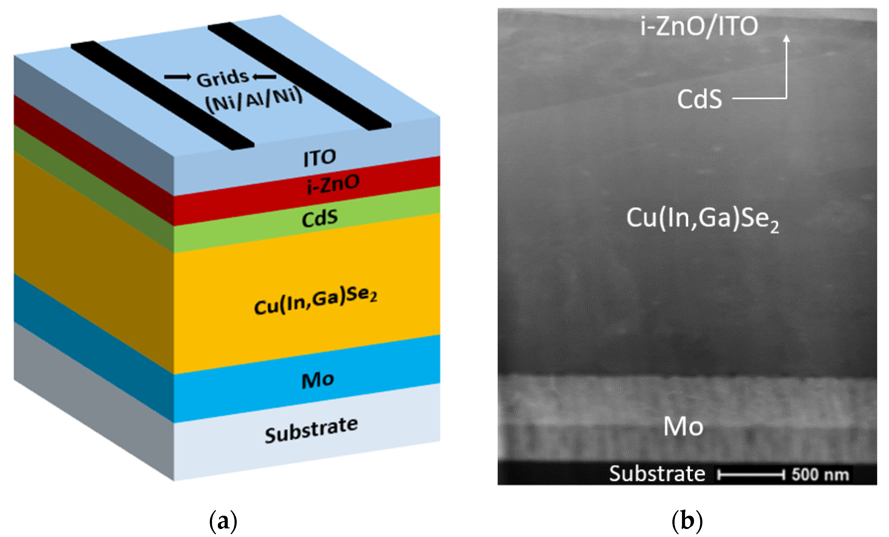
2. Materials and Methods

CIGS devices were fabricated on soda–lime glass (SLG) substrates with a SLG/Mo/CIGS/CdS/i-ZnO/ITO structure, using a three-stage co-evaporation process for the CIGS. First, a Mo (target 2.00” diameter × 0.250” thick, purity—99.95%) bilayer was deposited by DC magnetron sputtering. The bottom layer was formed at high argon pressure and the top layer at low pressure, resulting in a tensile/compressive stress dipole. After that, CIGS films were deposited using a three-stage co-evaporation process [16], followed as rapidly as possible by formation of a CdS layer using chemical bath deposition. The window layer (i-ZnO (target 2.00” diameter × 0.250” thick, purity—99.99%) and ITO (target 2.00” diameter × 0.250” thick, purity—99.99%) were deposited by RF sputtering at four different pressures (from 1 mTorr (0.13 Pa) to 7 mTorr (0.93 Pa)). After the i-ZnO/ITO deposition, half of the samples were soaked in deionized water (18.2 MΩ) at 50 °C for up to 24 h (referred to as water-soaked (WS) CIGS), whereas the other half were stored in a dry box until grid deposition (referred to as reference). Figure 1 shows the schematic diagram of a typical CIGS solar cell and a corresponding TEM image for a reference sample. The use of deionized water was intentional to avoid having unknown impurities mask potential ion migrations in the active layers of the devices. Finally, Ni/Al/Ni front contacts were deposited by electron–beam evaporation, and solar cells with an active area of 0.5 cm2 were defined by mechanical scribing using a razor blade. Additional test structures were also fabricated on silicon substrates for the i-ZnO/ITO bilayers in parallel to the device structures.
X-ray diffraction (XRD), spectroscopic ellipsometry, atomic force microscopy (AFM), and Hall effect measurements were used to characterize the properties of the i-ZnO/ITO layers by themselves. Time of flight secondary ion mass spectrometry (ToF SIMS) (ION TOF, Inc. Chestnut Ridge, NY, USA) was used to measure the compositional variation as a function of depth in the device. The photovoltaic characteristics were evaluated by external quantum efficiency (QE) measurements (QEX7, PV Measurements Inc., Point Roberts, WA, USA) and current density-voltage (J-V) measurements (IV5, PV Measurements Inc., Point Roberts, WA, USA), done under simulated AM 1.5 G with a light intensity of 100 mW/cm2 at 25 °C.

3. Results and Discussion

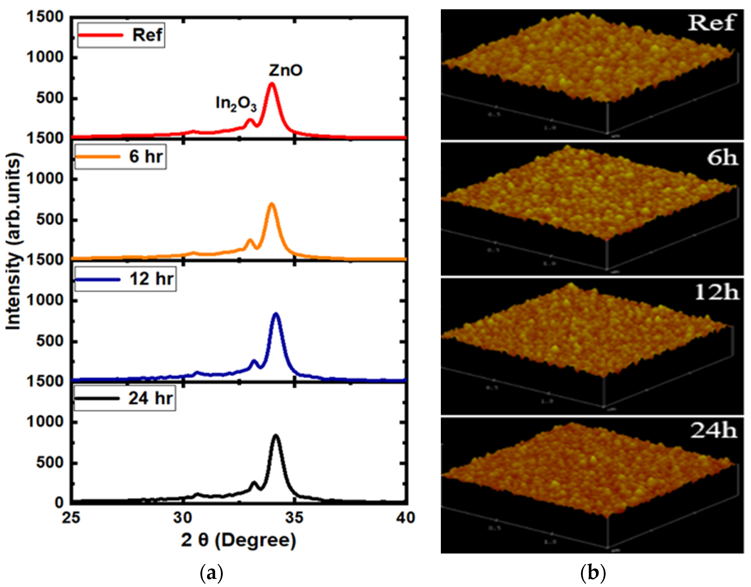
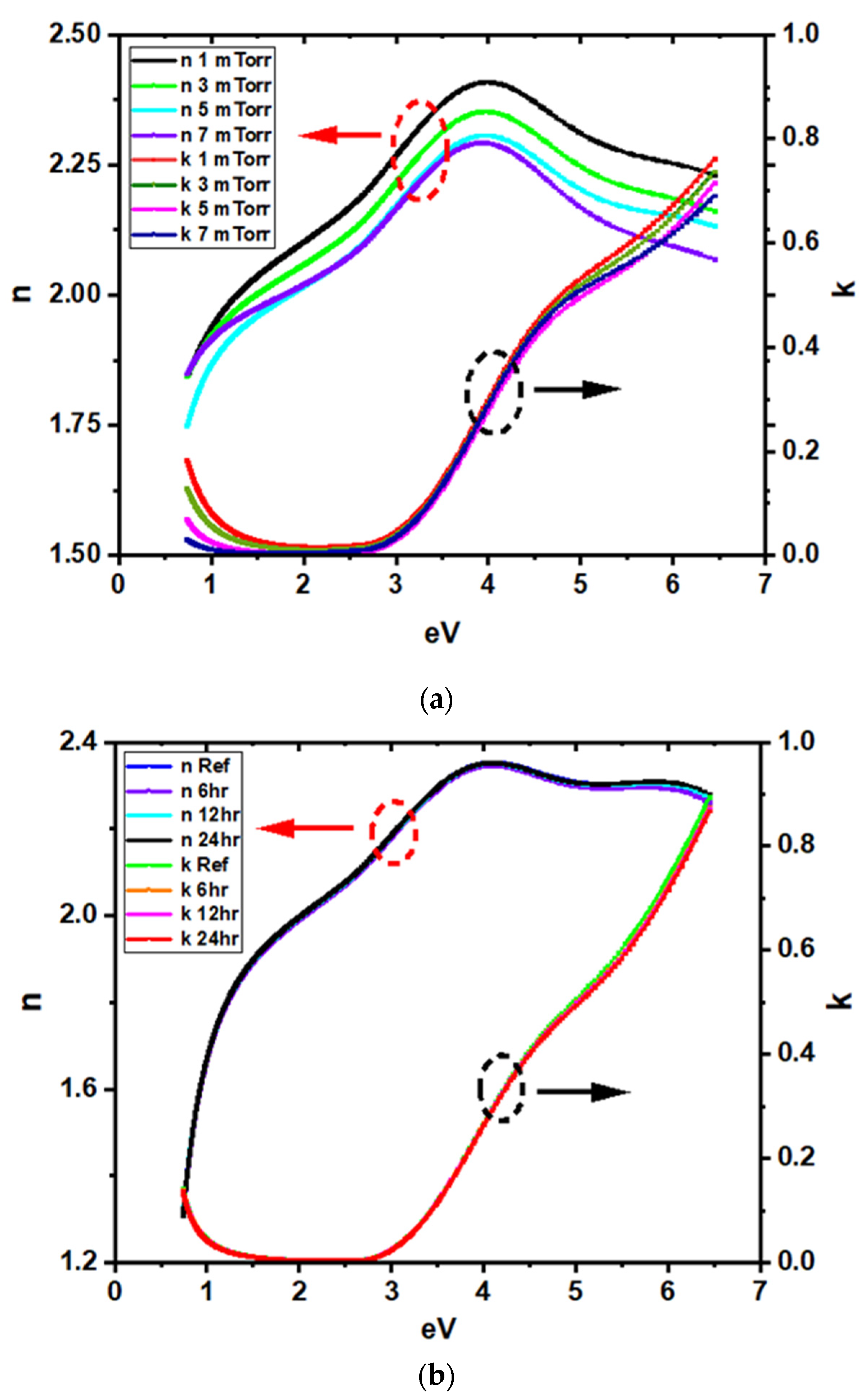
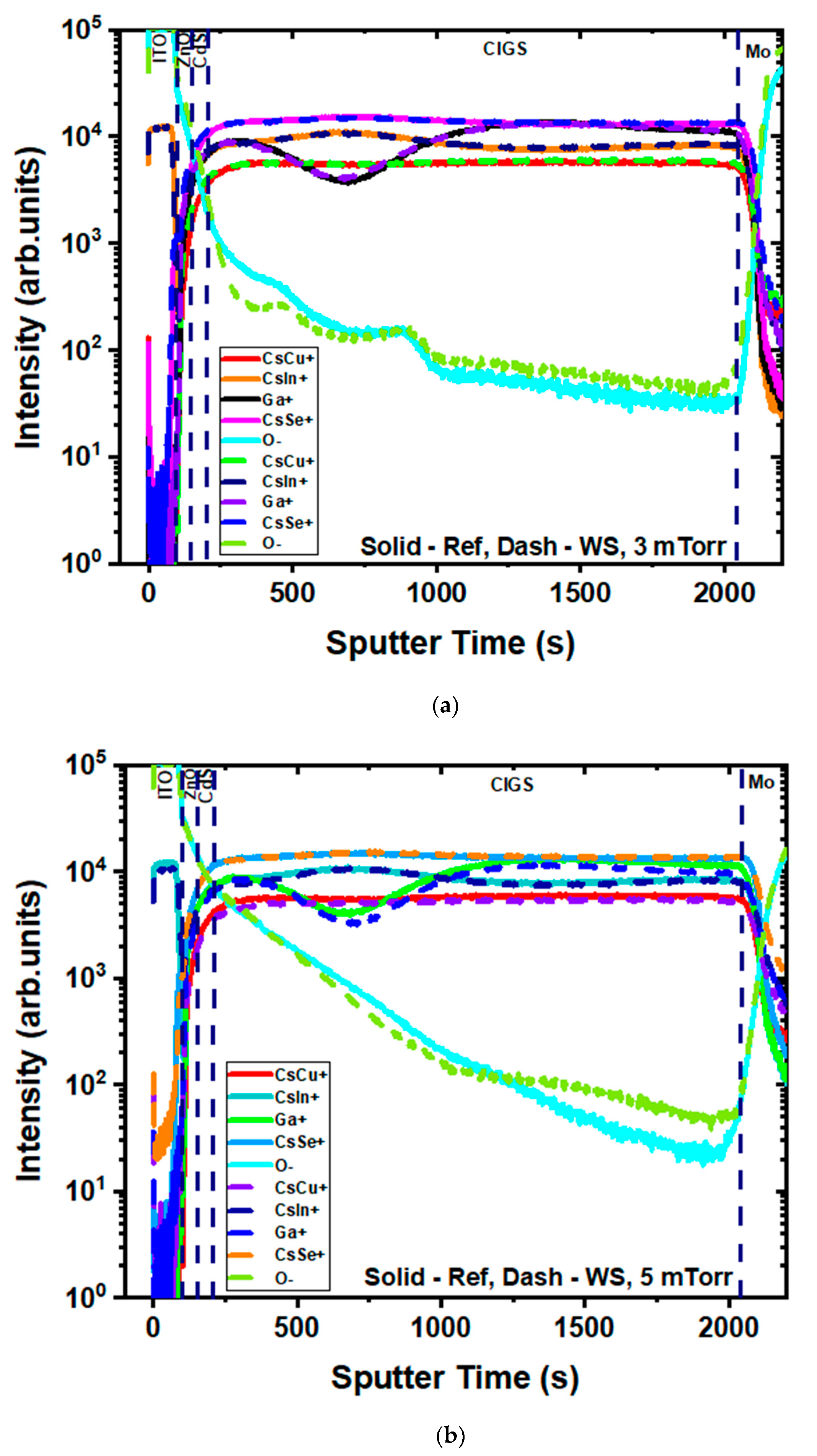
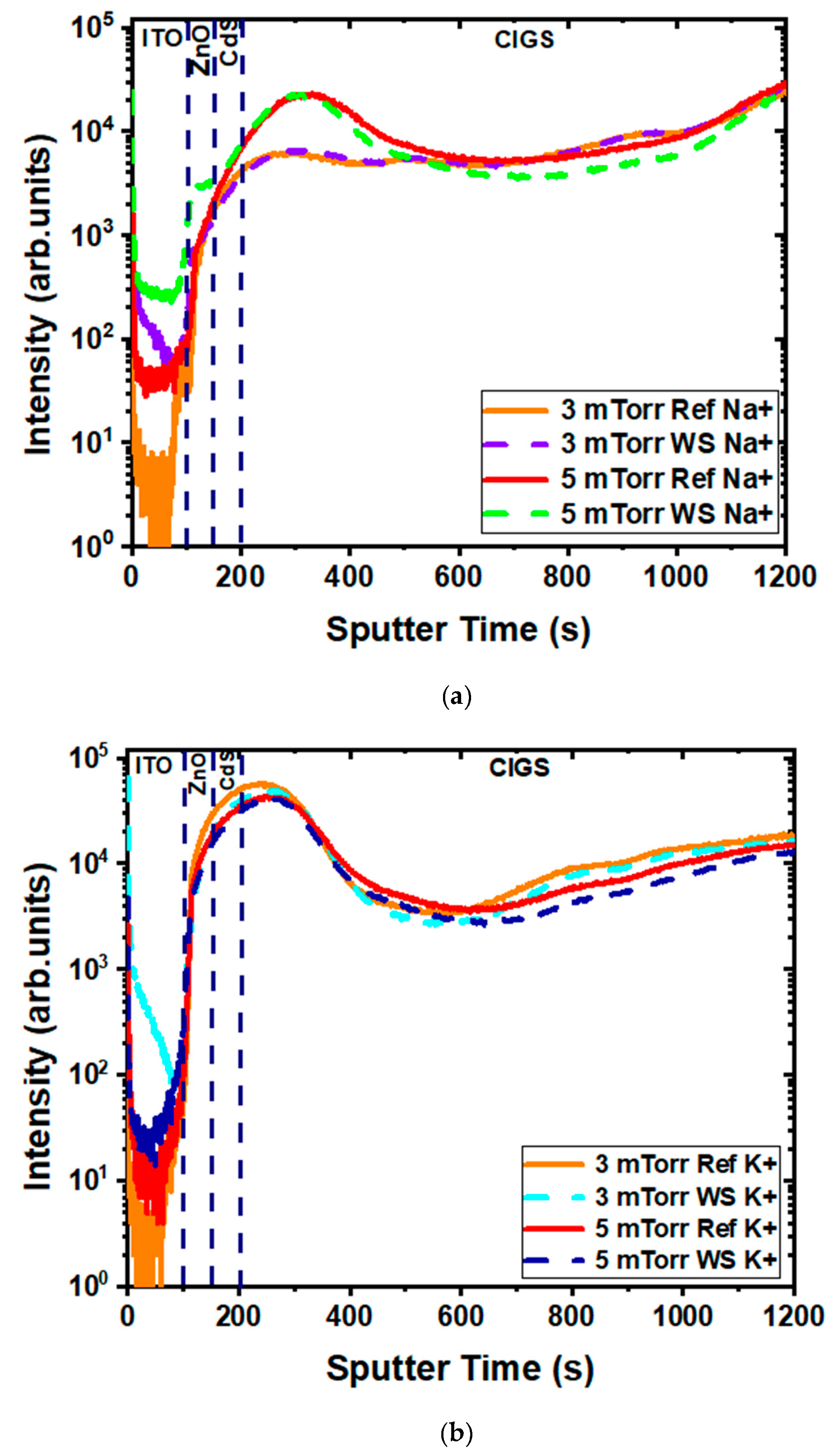
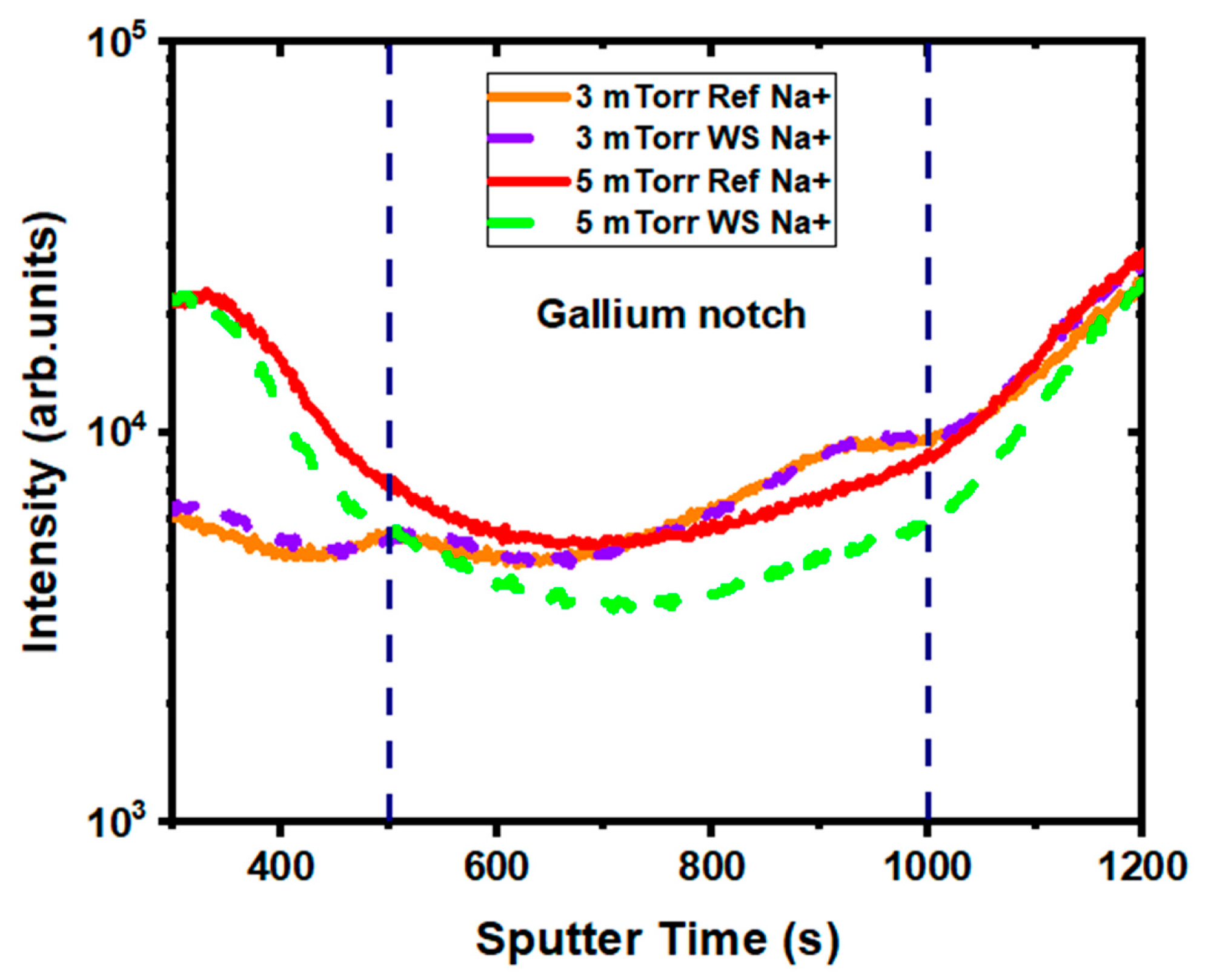
3.1. Effect of Water Ingress on the Window Layer

XRD measurements were performed before and after water soaking on silicon substrate, as shown in the case of the 5 mTorr samples in Figure 2. As expected for room temperature depositions, the films were mostly amorphous, but In2O3 and ZnO (ICDD) peaks were identified in both as-deposited and water-soaked samples. Further, XRD spectra did not show any noticeable change in peak position, peak intensity, preferential orientation, or broadening, before and after water soaking in the symmetric geometry XRD (θ\2θ) patterns. The peaks did not shift, implying that the strain did not vary with water soaking. A small change was observed in AFM and rms (Root Mean Square) roughness, with roughness decreasing from 3 nm (before water soaking) to 2 nm (after water soaking).
The as-deposited dielectric functions of i-ZnO/ITO films were obtained by spectroscopic ellipsometry at various pressures (1 mTorr, 3 mTorr, 5 mTorr, and 7 mTorr) on Si substrates (Figure 2). The dielectric functions of the ITO were parametrized by using a combination of Tauc-Lorentz, Gaussian, and Drude oscillator functions [17]. The overall same distinct features were observed regardless of the deposition pressure and water soaking duration. However, one can see that the refractive index decreased with increasing sputtering pressure (Figure 3a), suggesting a decreasing film density with increasing pressure [18]. Furthermore, the extinction coefficient at low energy, modeled via a Drude oscillator, increased at lower pressure, indicating higher film conductivity. On the other hand, the conductivity obtained from the Drude oscillator remained the same at a given pressure, even after water soaking for 24 h (Figure 3b). Both these facts were confirmed by Hall effect measurements. The electrical properties of the films, such as carrier concentration, mobility, and resistivity, did not show any significant change after water soaking. The average mobility, carrier concentration, and resistivity were found to be around 27 cm2/Vs, 8 × 1020 cm–3 and 2 × 10⁻⁴ Ωcm, respectively, whether before or after water soaking. A small change in the dielectric functions was observed at high energy after water soaking, consistent with a slight change in surface roughness observed by AFM. The change in surface roughness might have been due to the water soaking, but also might have been due to the measurement being taken on a slightly different location of the sample.
Overall, this indicates that the i-ZnO/ITO films have different properties as a function of deposition pressure (higher conductivity and density at low pressure), but do not degrade even after 24 h of water soaking.

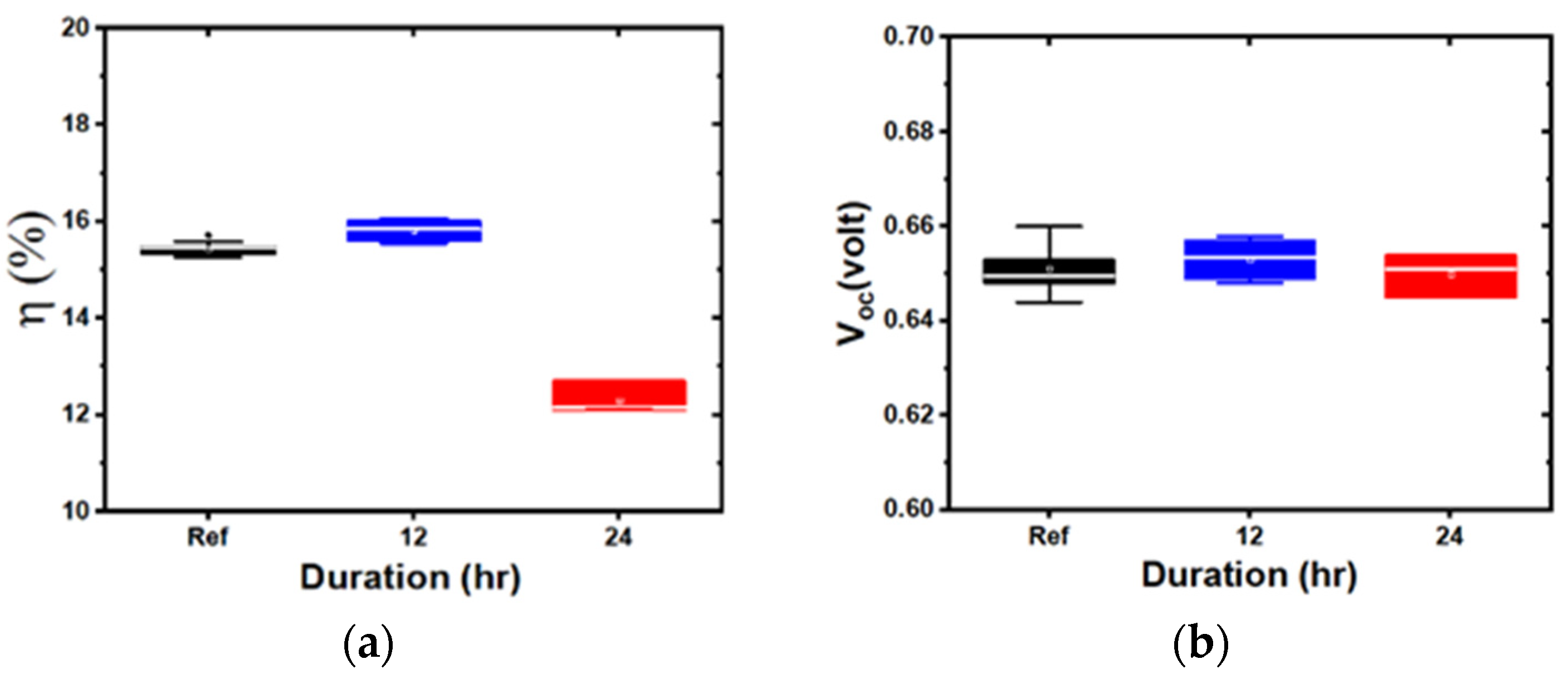
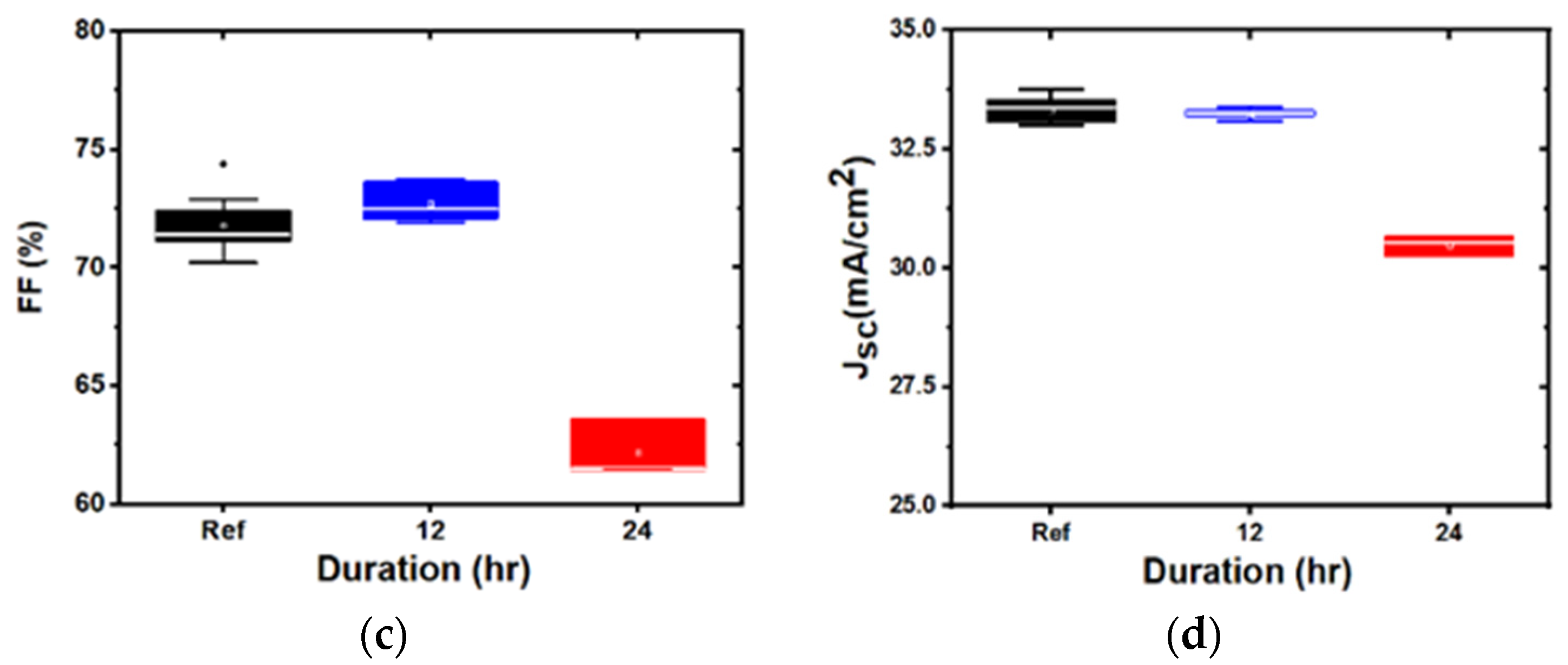
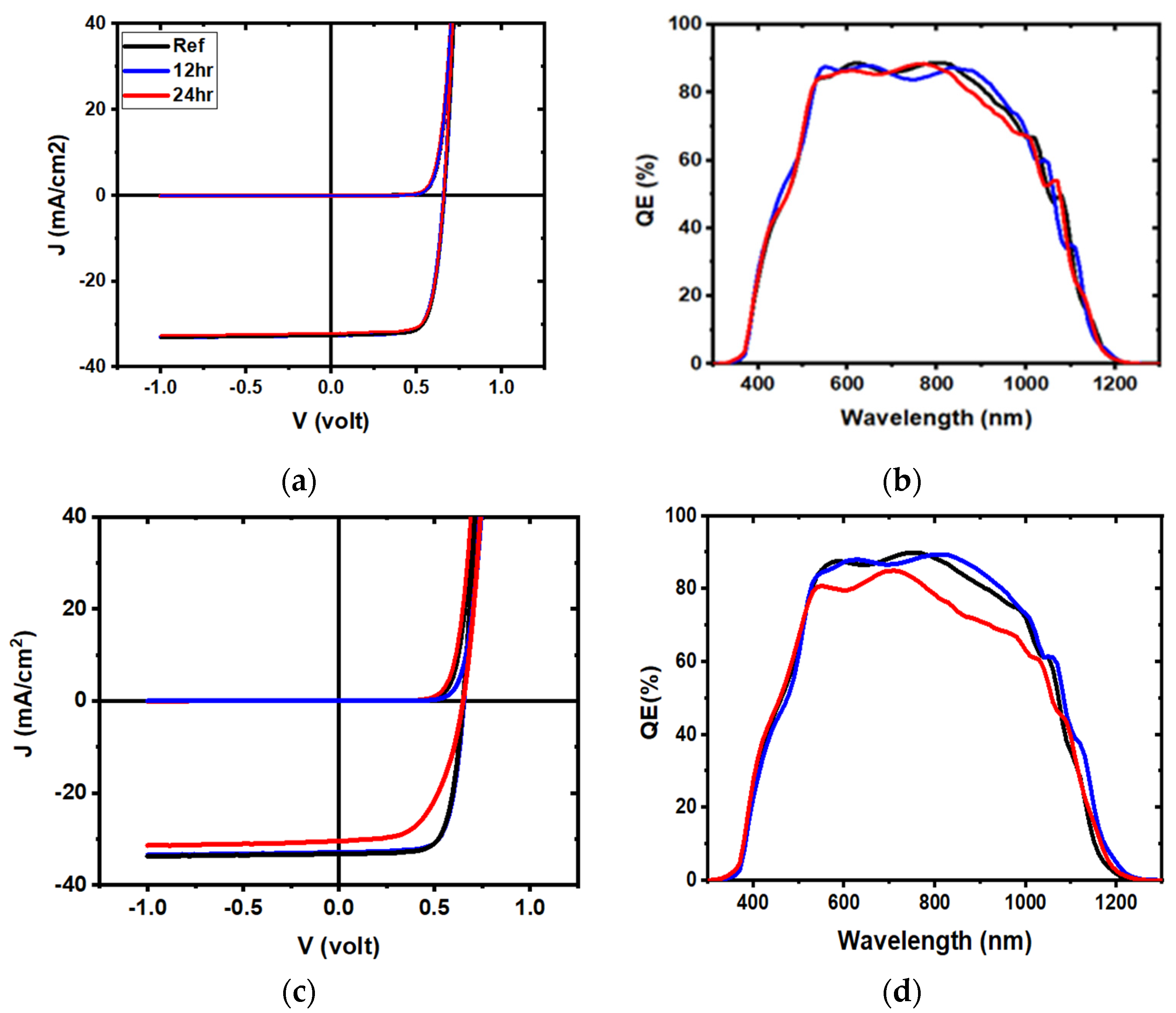
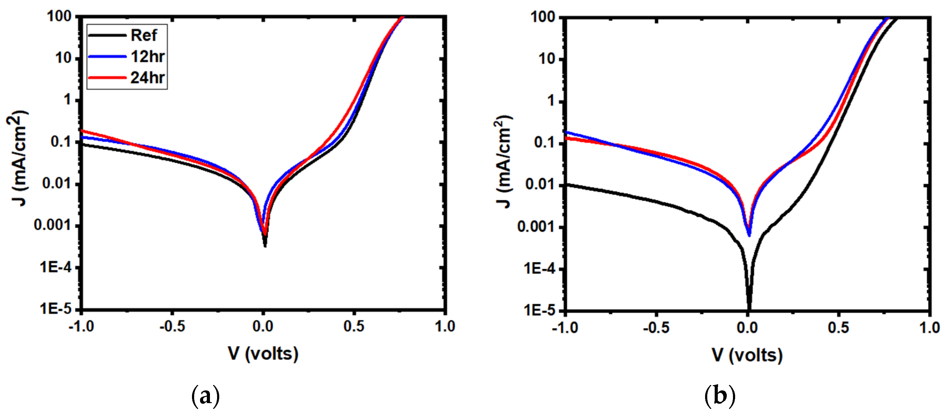
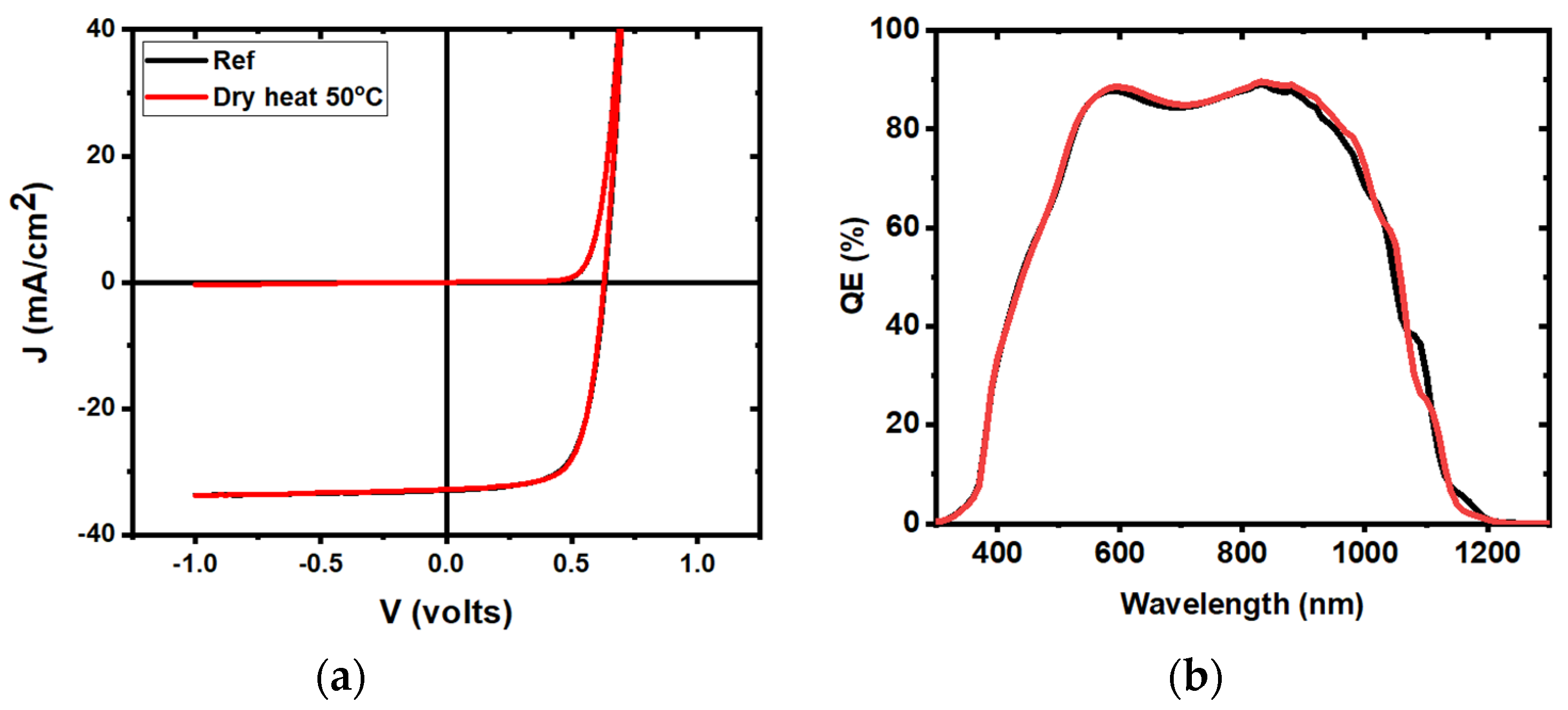
3.2. Effect of Water Soaking on Devices

Devices with window layers deposited at 3 mTorr and 5 mTorr were immersed in deionized water for 12 or 24 h. Devices were also made with lower pressure (1 mTorr) and higher pressure (7 mTorr) TCO, but initial device performance was poor due to the lower quality of the layers (low transmission for 1 mTorr and low conductivity for 7 mTorr). Afterwards, grids were deposited, and the devices were scribed to isolate them. The devices were then tested and compared to reference samples.
Representative box plots, comparing the device characteristics of the baseline and water-soaked structures with the ITO deposited at 3 mTorr and 5 mTorr, are shown in Figure 4 and Figure 5, respectively. The samples showed either no degradation or significant degradation, depending on the ITO sputtering pressure. The overall performance remained similar in 3 mTorr samples. By contrast, the performance degraded for ITO deposited at 5 mTorr, after 24 h of water soak, mostly due to the degradation of JSC and FF. Interestingly, and contrary to previous damp heat studies, no change in VOC was observed. We also observed that the 1 mTorr devices did not degrade, while the 7 mTorr devices degraded, indicating that there is a critical pressure at which devices start to degrade (in our case, above 3 mTorr).
Figure 6 shows representative current-voltage and external quantum efficiency (QE) curves for devices, while Figure 7 represents the dark J-V curves in semi-log plots. The currents calculated from QE measurement by integration were compared to the JSC measurement, and were found to be similar (Table 1). There was almost no change for the ITO deposited at 3 mTorr, while there was an overall decrease in current at all wavelengths for the ITO deposited at 5 mTorr, after 24 h. Additionally, a lack of change was noted in the ITO deposited at 5 mTorr, after 12 h. While water soaking for 12 h had little effect, after 24 h, the ITO deposited at 5 mTorr showed (Table 2) a higher reverse saturation current density (J0) and an increase in diode quality factor (A). Furthermore, there was a clear loss of collection at the maximum power point after 24 h of water soaking (QE curves, Figure 6d). Voltage-dependent current collection was observed in the 5 mTorr sample, whereas no dark-to-light cross-over was observed in either case. An increase in series resistance and shunt conductance also appeared, directly impacting the fill factor [19].
These devices were also investigated by secondary ion mass spectroscopy (SIMS) depth profiles. The matrix elements of each layer were characterized (Figure 8), and no significant change was observed for Cu, In, Ga, or Se, as expected. Interestingly, the oxygen profile also did not show any change before and after water soaking, whatever the ITO fabrication process was. The oxidation of the layers or interfaces was, therefore, not the reason for device degradation.
The potential degradation mechanism could also be due to impurities localized at grain boundaries that can become transient with elevated heat and water. Since alkalis—and sodium and potassium in particular—are predominant and critical impurities in CIGS solar cells, depth profiles for Na and K were, therefore, measured for the same samples and are plotted in Figure 9. While some small variances were observed in the 3 mTorr sample, the similarity before and after water soaking explains why minimal degradation was observed.
For the 5 mTorr sample, the profiles seemed similar overall, too, except close to the gallium notch in the CIGS (Figure 10), where a lower concentration of alkali was present after water soaking. This loss of alkaline species in this specific region of CIGS, where recombination can be predominant, could explain the degradation in the 5 mTorr devices after water soaking. Indeed, a previous experiment showed that the migration of alkali-elements, like Na and K, causes a decrease in shunt resistance [20]. Another interesting aspect of the Na profile was the appearance of a slightly higher concentration of Na in the ITO after water soaking. Since Na tends to degrade ITO properties [1], this might have also affected the space charge region and led to voltage-dependent current collection for the 5 mTorr water-soaked samples.
To assess whether this diffusion process was solely due to temperature, additional samples were fabricated with 5 mTorr ITO layers, soaked for 24 h in water at 50 °C, and compared to samples heated at 50 °C under ambient air, as well as reference samples. As seen previously, significant performance loss was observed in the water soaking samples (Figure 6c,d), but not for samples held at 50 °C in dry conditions for 24 h (Figure 11). This implies that the degradation was due to moisture rather than heat, suggesting that this was not a purely diffusion-based change. These new results are similar to the ones observed in classical damp heat studies, where humidity plays a significant role in device degradation and devices remain generally stable when heated in a moisture free environment, as seen in several references [21,22].

4. Conclusions

The deposition pressure of the ITO layer produced a significant change in the resistance of the final device to water damage. It was observed that the ITO layers themselves did not change because of the water soaking process, but that the alkali profile was modified after water soaking for the high-pressure deposition processes. The primary difference expected between any two thin films deposited by sputter deposition at different pressures is a change in reflected neutral bombardment of the growing film. Sputtering ITO in Ar would be expected to result in a significant number of Ar atoms reflected from the target with substantial energies. In addition, there is the possibility of the formation of negative oxygen ions at the target surface, which would be accelerated to the target potential. Increased gas pressure leads to increased gas scattering and a lower impact energy on the growing film. This, in turn, reduces the compressive stress in the deposited layer or converts the stress to tensile. We hypothesize that, in this case, the higher sputtering pressure led to a tensile stress in the ITO with relatively open grain boundaries. This could have permitted increased water ingress to the underlying junction and, consequently, increased degradation, in agreement with our previous study of exposure of the CIGS itself to water. It is therefore assumed that the alkali diffusion process, coming in the direction of the substrate to the top layer, is modified and causes a decrease in shunt resistance and an increase in series resistance, which ultimately decreases the FF. It is, of course, possible that additional processes, including notable changes in terms of chemical bounding and surface modification, might be affected by this treatment and affect device properties.

Author Contributions

Conceptualization, S.M. and A.R.; validation, D.P., S.K., B.B., G.R., S.A. and S.S.; formal analysis, S.M., A.R., D.P., S.K., B.B., G.R., S.S.A. and S.S.; writing—original draft preparation, S.M., A.R., D.P., S.K., B.B., G.R., S.S.A. and S.S.; writing—review and editing, S.M., A.R., D.P., S.K., B.B., G.R., S.S.A. and S.S.; supervision, S.M. and A.R.; funding acquisition, S.M. and A.R. All authors have read and agreed to the published version of the manuscript.

Funding

This research was supported by the Department of Energy, Contract No. DE-EE0007141.

Conflicts of Interest

The authors declare no conflict of interest.

References

  1. Theelen, M.; Daume, F. Stability of Cu (In, Ga) Se2 solar cells: A literature review. Sol. Energy 2016, 133, 586–627. [Google Scholar] [CrossRef]
  2. Igalson, M.; Wimbor, M.; Wennerberg, J. The change of the electronic properties of CIGS devices induced by the ‘damp heat’treatment. Thin Solid Films 2002, 403, 320–324. [Google Scholar] [CrossRef]
  3. Lee, D.W.; Cho, W.J.; Song, J.K.; Kwon, O.Y.; Lee, W.H.; Park, C.H.; Park, K.E.; Lee, H.; Kim, Y.N. Failure analysis of Cu (In, Ga) Se2 photovoltaic modules: Degradation mechanism of Cu (In, Ga) Se2 solar cells under harsh environmental conditions. Prog. Photovolt. Res. Appl. 2015, 23, 829–837. [Google Scholar] [CrossRef]
  4. Guillen, C.; Herrero, J. Stability of sputtered ITO thin films to the damp-heat test. Surf. Coat. Technol. 2006, 201, 309–312. [Google Scholar] [CrossRef]
  5. Sundaramoorthy, R.; Pern, F.; DeHart, C.; Gennett, T.; Meng, F.; Contreras, M.; Gessert, T. Stability of TCO window layers for thin-film CIGS solar cells upon damp heat exposures: Part II, reliability of photovoltaic cells, modules, components, and systems II. Int. Soc. Opt. Photon. 2009, 7412, 74120J. [Google Scholar]
  6. Karki, S.; Paul, P.; Deitz, J.I.; Poudel, D.; Rajan, G.; Belfore, B.; Danilov, E.O.; Castellano, F.N.; Grassman, T.J.; Arehart, A. Degradation mechanism in Cu (In, Ga) Se 2 material and solar cells due to moisture and heat treatment of the absorber layer. IEEE J. Photovolt. 2019, 9, 1138–1143. [Google Scholar] [CrossRef]
  7. Karki, S.; Deitz, J.I.; Rajan, G.; Soltanmohammad, S.; Poudel, D.; Belfore, B.; Bhandari, G.; Grassman, T.J.; Rockett, A.; Marsillac, S. Impact of water ingress on molybdenum thin films and its effect on Cu (In, Ga) Se 2 Solar Cells. IEEE J. Photovolt. 2019, 10, 696–702. [Google Scholar] [CrossRef]
  8. Wennerberg, J.; Kessler, J.; Stolt, L. Cu (In, Ga) Se2-based thin-film photovoltaic modules optimized for long-term performance. Solar Energy Mater. Sol. Cells 2003, 75, 47–55. [Google Scholar] [CrossRef]
  9. Lee, D.-W.; Cho, W.-J.; Jang, C.-I.; Song, J.-K.; Park, C.-H.; Park, K.-E.; Ryu, J.-S.; Lee, H.; Kim, Y.-N. Damp heat and thermal cycling-induced degradation mechanism of AZO and CIGS films in Cu (In, Ga) Se2 photovoltaic modules. Curr. Appl. Phys. 2015, 15, 285–291. [Google Scholar] [CrossRef]
  10. Feist, R.; Rozeveld, S.; Mushrush, M.; Haley, R.; Lemon, B.; Gerbi, J.; Nichols, B.; Nilsson, R.; Richardson, T.; Sprague, S. Examination of lifetime-limiting failure mechanisms in CIGSS-based PV minimodules under environmental stress. In Proceedings of the 2008 33rd IEEE Photovoltaic Specialists Conference, San Diego, CA, USA, 11–16 May 2008; pp. 1–5. [Google Scholar]
  11. Osterwald, C.R. Terrestrial Photovoltaic Module Accelerated Test-to-Failure Protocol; National Renewable Energy Lab. (NREL): Golden, CO, USA, 2008. [Google Scholar]
  12. Thompson, C.P.; Hegedus, S.; Carcia, P.; McLean, R.S. The effects of device geometry and TCO/Buffer layers on damp heat accelerated lifetime testing of Cu (In, Ga)Se2 Solar Cells. IEEE J. Photovolt. 2012, 3, 494–499. [Google Scholar] [CrossRef]
  13. Daume, F.; Puttnins, S.; Scheit, C.; Zachmann, H.; Rahm, A.; Braun, A.; Grundmann, M. Damp heat treatment of Cu (In, Ga) Se2 solar cells with different sodium content. Materials 2013, 6, 5478–5489. [Google Scholar] [CrossRef] [PubMed]
  14. Malmström, J.; Wennerberg, J.; Stolt, L. A study of the influence of the Ga content on the long-term stability of Cu (In, Ga) Se2 thin film solar cells. Thin Solid Films 2003, 431, 436–442. [Google Scholar] [CrossRef]
  15. Schmidt, M.; Braunger, D.; Schäffler, R.; Schock, H.; Rau, U. Influence of damp heat on the electrical properties of Cu (In, Ga) Se2 solar cells. Thin Solid Films 2000, 361, 283–287. [Google Scholar] [CrossRef]
  16. Noufi, R.; Gabor, A.M.; Tuttle, J.R.; Tennant, A.L.; Contreras, M.A.; Albin, D.S.; Carapella, J.J. Method of Fabricating High-Efficiency Cu (In, Ga)(SeS)2 Thin Films for Solar Cells. Google Patents U.S. 5,441,897, 15 August 1995. [Google Scholar]
  17. Fujiwara, H. Spectroscopic Ellipsometry: Principles and Applications; John Wiley & Sons: Hoboken, NJ, USA, 2007. [Google Scholar]
  18. Tseng, K.-S.; Lo, Y.-L. Effect of sputtering parameters on optical and electrical properties of ITO films on PET substrates. Appl. Surf. Sci. 2013, 285, 157–166. [Google Scholar] [CrossRef]
  19. Tosun, B.S.; Feist, R.K.; Gunawan, A.; Mkhoyan, K.A.; Campbell, S.A.; Aydil, E.S. Improving the damp-heat stability of copper indium gallium diselenide solar cells with a semicrystalline tin dioxide overlayer. Sol. Energy Mater. Sol. Cells 2012, 101, 270–276. [Google Scholar] [CrossRef]
  20. Theelen, M.; Hendrikx, R.; Barreau, N.; Steijvers, H.; Böttger, A. The effect of damp heat-illumination exposure on CIGS solar cells: A combined XRD and electrical characterization study. Solar Energy Mater. Sol. Cells 2016, 157, 943–952. [Google Scholar] [CrossRef]
  21. Theelen, M.; Beyeler, K.; Steijvers, H.; Barreau, N. Stability of CIGS solar cells under illumination with damp heat and dry heat: A comparison. Sol. Energy Mater. Solar Cells 2017, 166, 262–268. [Google Scholar] [CrossRef]
  22. Westin, P.-O.; Neretnieks, P.; Edoff, M. Damp heat degradation of CIGS-based PV modules. In Proceedings of the 21st European Photovoltaic Solar Energy Conference, Dresden, Germany, 4–8 September 2006; pp. 2470–2473. [Google Scholar]
Figure 1. (a) Schematic diagram of a typical copper indium gallium diselenide (CIGS) solar cell device. During testing, water arrived from the top. (b) STEM-HAADF image of a CIGS reference sample.
Energies 13 04545 g001
Figure 2. (a) X-ray diffraction pattern and (b) atomic force microscopy of the 5 mTorr reference and water-soaked samples, after water soaking for various durations.
Energies 13 04545 g002
Figure 3. Dielectric functions of (a) intrinsic zinc oxide/indium tin oxide (i-ZnO/ITO) deposited at various pressures and (b) i-ZnO/ITO deposited at 5mTorr, water-soaked for various durations.
Energies 13 04545 g003
Figure 4. Box plots of device parameters for indium tin oxide (ITO) deposited at 3 mTorr, soaked for different durations: (a) efficiency; (b): open circuit voltage; (c): fill factor; and (d): short circuit current density.
Energies 13 04545 g004
Figure 5. Box plots of device parameters for indium tin oxide (ITO) deposited at 5 mTorr, soaked for different durations: (a): efficiency; (b): open circuit voltage; (c): fill factor; and (d): short circuit current density.
Energies 13 04545 g005aEnergies 13 04545 g005b
Figure 6. Representative density-voltage (J-V) and quantum efficiency (QE) curves for 3 mTorr samples (a,b) and 5 mTorr samples (c,d), for reference (black) and water-soaked (12 h: blue, 24 h: red) devices.
Energies 13 04545 g006
Figure 7. Representative semi-log plots of the dark J-V curves for 3 mTorr samples (a) and 5 mTorr samples (b) for reference (black) and water-soaked (12 h: blue, 24 h: red) devices.
Energies 13 04545 g007
Figure 8. Secondary ion mass spectroscopy (SIMS) depth profiles for the main element for both the (a) 3 mTorr and (b) 5 mTorr experimental sets (reference: solid lines; 24 h water-soaked: dashed lines).
Energies 13 04545 g008
Figure 9. SIMS depth profiles of Na+ (a) and K+ (b) in the reference (solid) and 24 h water-soaked (dash) samples for the 3 mTorr and the 5 mTorr experimental set.
Energies 13 04545 g009
Figure 10. Detailed SIMS depth profile in the bulk of copper indium gallium diselenide (CIGS) of Na+ in the reference (solid) and 24 h water-soaked (dash) samples, for the 3 mTorr and the 5 mTorr experimental set.
Energies 13 04545 g010
Figure 11. Representative J-V (a) and QE (b) curves for 5 mTorr samples heated in dry conditions at 50 °C (red curve), compared to reference samples (black curve).
Energies 13 04545 g011
Table 1. Solar cell parameters of representative cells shown in Figure 4 and Figure 5.
Sample VOC
(V)
JSC
(mA/cm2)
JSC (QE)
(mA/cm2)
FF
(%)
η
(%)
3 mTorrRef0.6632.732.674.416.0
12 h WS0.6632.632.674.316.0
24 h WS0.6632.332.474.215.8
5 mTorrRef0.6533.133.073.015.6
12 h WS0.6432.932.972.815.3
24 h WS0.6430.530.662.012.1
Table 2. Diode parameters (Dark J-V) of representative cells shown in Figure 4 and Figure 5.
Sample J0 (mA/cm2)Diode Factor (A)RSH (kΩ·cm2)RS (Ω·cm2)
3 mTorrRef2.5 × 10−91.81.2 × 1040.4
12 h WS4.0 × 10−91.81.3 × 1040.5
24 h WS5.0 × 10−91.92.4 × 1040.5
5 mTorrRef2.5 × 10−91.77.5 × 1030.4
12 h WS8.0 × 10−91.88.0 × 1030.5
24 h WS8.0 × 10−92.01.4 × 1030.6

