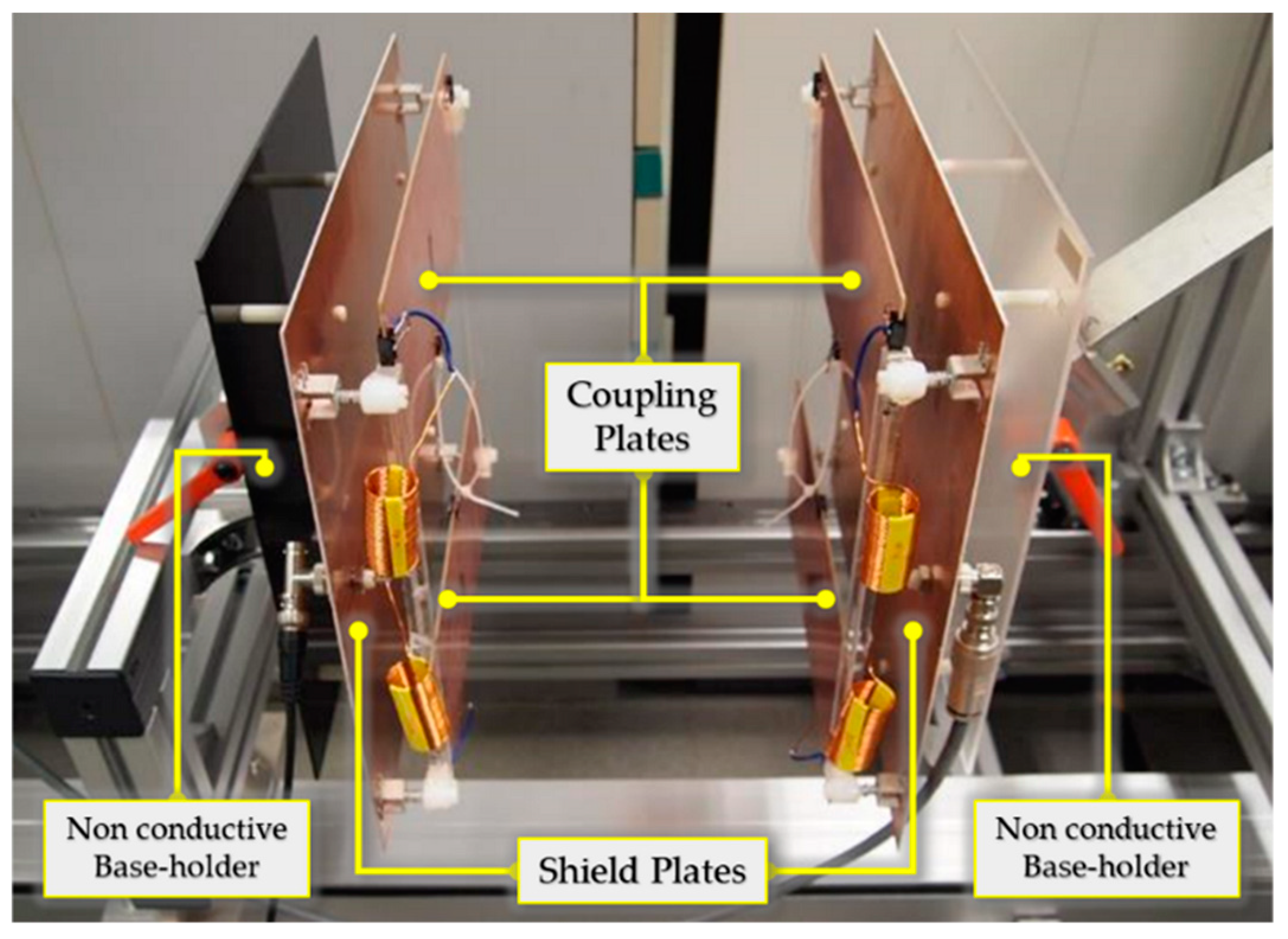
The proposed shielded-CPT structure is constructed as a conventional CPT coupling-plate interface with two additional plates behind each side. The coupling structure builds a six-plate CPT system consisting of a power transfer part and a shielding part as seen in
Figure 1. With this configuration, the circuit parameter is optimized to the required power and efficiency, the size and distance of the coupling in consideration to the safety level of air breakdown voltage and the stray of EF. By introducing the extra plates, the EF-emission characteristic was observed through field-simulation and hardware experiments [
23,
24]. In these studies, the six-plate CPT system shows that the EF emission has been reduced significantly compared to the four-plate systems [
26].
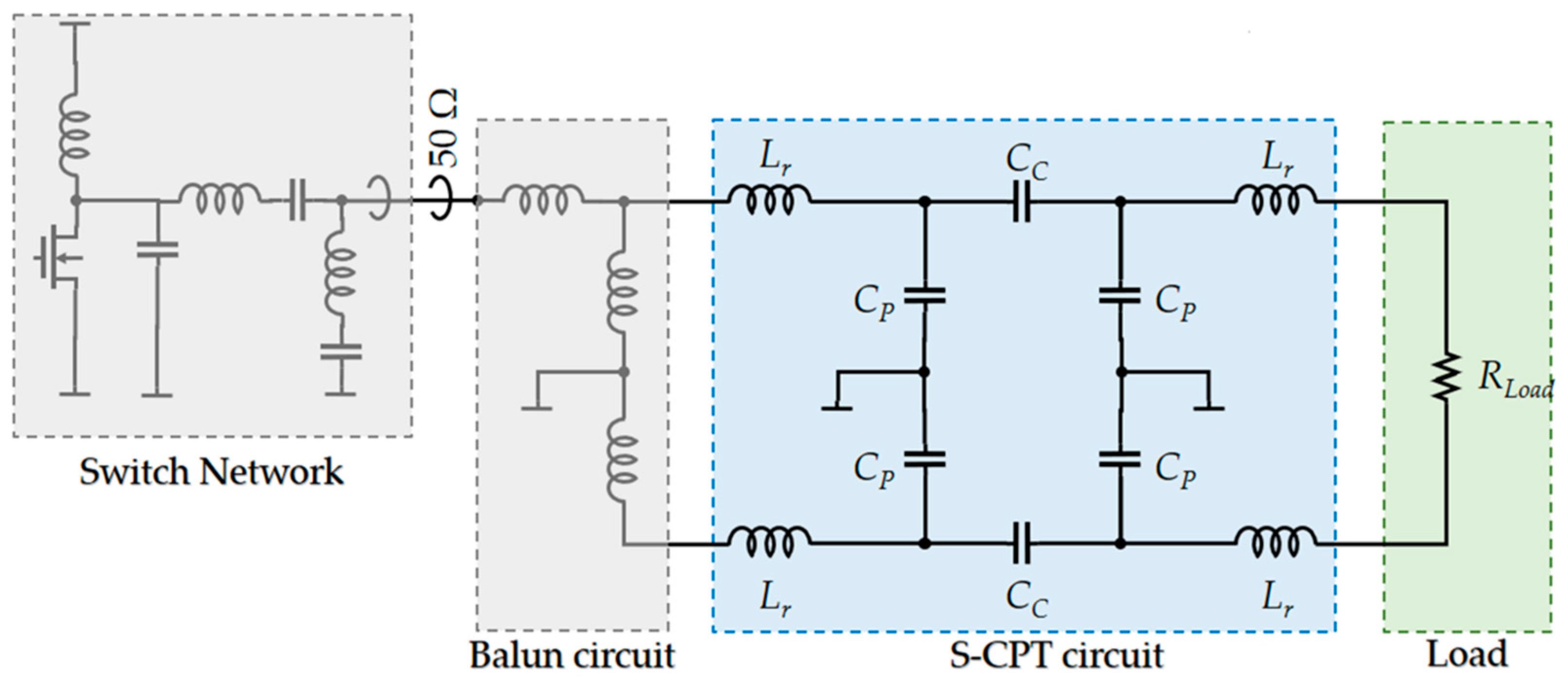
The circuit model of the complete shielded-CPT system is shown in
Figure 2. Four parts of the circuit model comprise a WPT system with a capacitive coupling interface. A switch network can be implemented by a single-ended Class-E power amplifier, half-bridge, or full-bridge inverter system [
27,
28,
29,
30]. A 50 Ω coaxial cable is used in the proposed system, and a balanced-to-unbalanced (Balun) transformer is coupled to the resonant inductors, providing a balanced condition of the voltage waveform and a stable ground reference to the coupling system [
31]. For simplicity of modeling, these two parts will be omitted in the scaling-factor analysis.
2.1. Circuit Model Analysis of the Shielded-CPT System
Figure 3 presents the analysis of the coupling interface of the proposed shielded-CPT system. The input-voltage source,
V0, produces a sinewave alternate current (AC) voltage that is applied to the input terminal of the shielded-CPT circuit. Accordingly, the resonant frequency is tuned by the value of the series-resonant inductor,
Lr, coupling capacitance,
CC, and parasitic capacitance,
CP, on the primary and secondary sides. The load resistance,
RLoad, is connected through the resonant inductors in the secondary side. As an assumption, the circuit topology involves of symmetry parameters for both placement and size.
The shielded-CPT circuit can be analyzed through three approximations. First, the primary (transmitter)-side impedance can be calculated under the assumption that all components on the primary side are modeled by a single parallel resistance,
RL, if a resonant condition occurs between them. Next, the secondary (receiver)-side impedance was assumed to be in a resonant condition with the receiver side; thus, the circuit is modeled by a single parallel resistance,
RL. The last approximation is a combination of the previous two, namely, the primary and secondary impedances match. Secondary-side-impedance-matched analysis is used for this paper.
Figure 4 illustrates the simplified circuit model for the process of analyzing the coupling capacitance,
CC. It consists of a single input-voltage source,
V0, with frequency
f, connected to the series-resonant inductor,
L, with equivalent series resistance (ESR),
RS. The circuit is coupled with the parasitic capacitance,
CP, in parallel with the coupling capacitance,
CC. here we assume that the secondary side has a resonant condition. The load resistance
RLoad and the L-matching circuit can be simplified as the load,
RL.
Using the circuit diagram in
Figure 4, Equation (1) is obtained based on the sinusoidal approximation for the
I1 current loop with angular frequency,
ω, using Kirchhoff laws (KCL):
In addition, applying KCL to the
I2 loop yields the relationship:
By substituting this term into (1),
I1 is
Under the resonant condition, the corresponding impedance will be purely resistive. Thus, the imaginary part of the total impedance of the circuit equals zero and the resonant inductance
L of the circuit can be calculated as
From
Figure 3, the stress voltage
V1 across the shield plate is found as
where
V0 is the input voltage,
RS is the ESR,
jωL is the inductor reactance, and
I1 is the current. Using (4),
V1 becomes
2.2. Optimization for Minimal Loss by Impedance Matching
The complete system topology of
Figure 3 is rearranged with
R0 as the internal characteristic resistance of the power source in
Figure 5. An AC-input voltage is applied to the resonant-circuit input. In this analysis, we assume that the total impedance of the coupling interface and the secondary side of the shielded-CPT are matched to
RL’. To attain a maximum power transfer, the total reflected output impedance must equal the input impedance of the circuit [
32]. This relationship is shown in (8):
By multiplying both the numerator and the denominator by
, we have
The reactive part of the circuit will be cancelled when it is in the resonant condition. Thus, the matching impedance state can be acquired as
While the values of capacitance
C and inductance
L can be acquired from the quality factor
Q of the components
The maximum value can be obtained using a derivative method. Therefore, the response to the load resistance
RL from (11) can be calculated by
From (14) and (15), the relationship between the load resistance,
RL’, and the internal characteristic resistance,
R0, can then be obtained as
Thus, the optimum impedance-matching condition can be obtained when the load resistance,
RL’, is twice the internal characteristic resistance,
R0. Using the KCL method, the gain of the circuit in
Figure 5 can be defined as
Substituting (11) and (16) into (17), we obtain
For analysis, the parameter of the circuit model is then defined to obtain a correlation in the capacitance, inductance, and circuit gain to the various load values. A square plate 10 cm in height and width achieves a coupling capacitance of 8.9 pF within 1 cm of the gap (see
Table 1). The behaviors of the capacitance, inductance, and the circuit gain under various values of impedance are illustrated in
Figure 6 and
Figure 7.
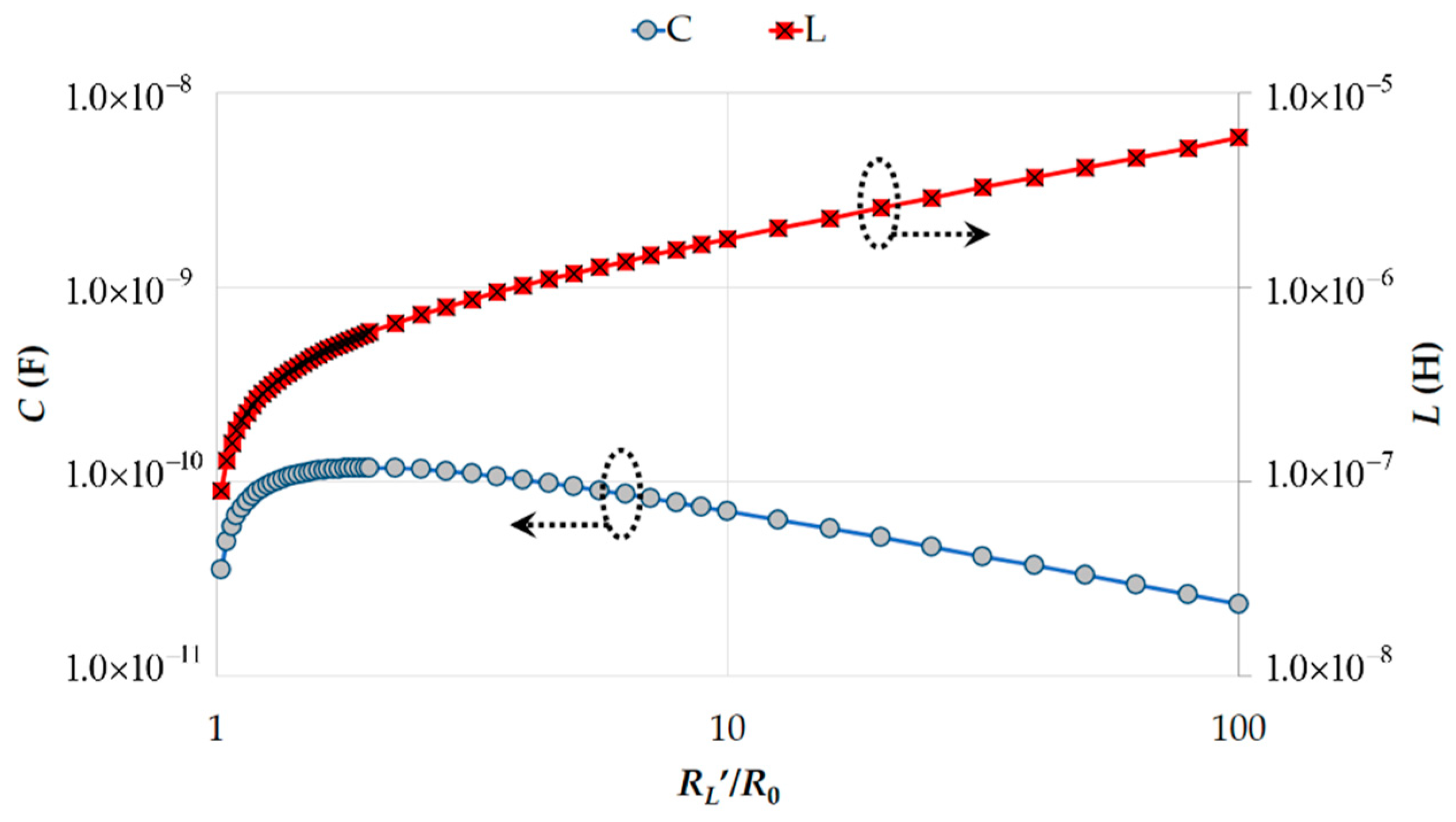
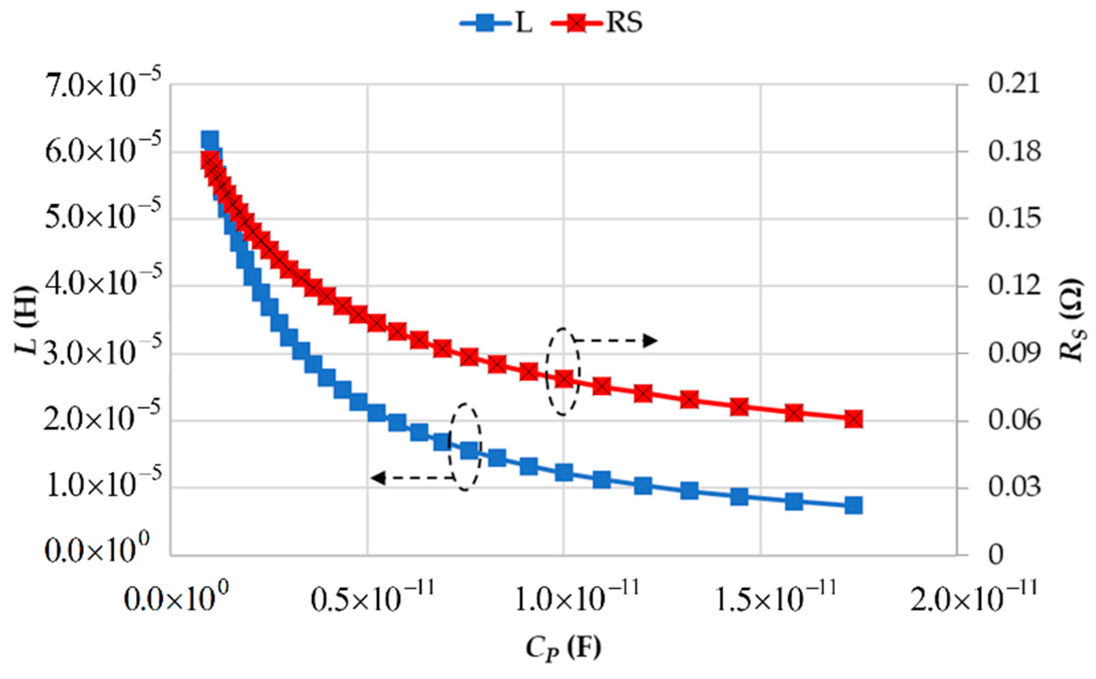
In
Figure 6, the shield parasitic capacitance
CP becomes large to obtain a thin coupler unit. However, to develop a large ratio between the load resistance and the internal series resistance,
RL’/
R0, the shield capacitance
CP should be small. Thus, there is a trade-off relationship between the unit thickness and output voltage (
Figure 7). With the increase of the load resistance, the load voltage,
VL, increases by a gradient of 1. By contrast, the load current decreases by gradient of −1. On the other hand, a large capacitance requires a small
RL’ and the shield capacitance value is limited to 2 for
RL’/
R0. A double-
LC-resonant-matching system (
LCLC circuit) may solve this problem.
Figure 8 shows the relationship between the resistance ratio and power loss of the inductor. With increasing
RL’,
RS rises because the inductor value increases, but
IL decreases. Thus, the loss in the inductor,
PS, decreases with increasing
RL’ because
PS is given by
IL2RS and the gradients in the log-log plot are roughly 1/2 and −1 for
RS and
IL, respectively. Therefore,
PS decreases with increasing
RL’ with a gradient of −3/2 in log-log plot (see
Figure 9).
2.3. Resonant Inductor Optimization for Minimal Loss
In this subsection, the ESR value of the inductor is investigated. Inductors can be constructed using many types of core materials; one is an air-core-type inductor that uses any non-magnetic material as its core to reduce core losses, i.e., eddy current & stray losses, especially when the operating frequency is very high. However, the use of a non-magnetic core also reduces inductance. Another type is a toroidal-core inductor, the core of which is made from a ferromagnetic material. The advantage of this circular core is that the magnetic field contains extremely low magnetic-flux leaks inside the core. The magnetic field at the core is higher because of a low leakage flow; hence, a toroidal-core inductor will have a higher inductance than a rod or bar-shaped core of the same material [
32,
33].
Figure 10 shows the dimensions and parameters of a toroidal-core inductor.
The core inductance can be acquired as
where
N is the number of turns,
µ is the core-material permeability,
S is the core thickness,
l is the wire length,
R and
r represent the core radius and core thickness radius, respectively. The series resistance in the inductor is
Thus, the series resistance
RS can be written as
where
ɸ and
ρ represent the thickness and resistivity of the wire, respectively. The series inductance is
Because the current flows through an inductor, its ESR consumes some power.
Figure 11 shows the circuit model used to analyze the power loss in a resonant inductor without considering parasitic capacitance, CP. An AC voltage source is connected in series with the ESR RS, the inductance
LS, the coupling capacitance
CC, and the load resistance
RL.
The power loss of the impedance-matching inductor,
PS, is defined by
by substituting
RS from (23) and (24) into (25),
PS can be calculated as
From (26), the relationship between the coupling capacitance,
CC, and the power loss of the matching inductor,
PS, is illustrated in
Figure 12. Amplification of the coupling capacitance results in inductance drops. In addition, the ESR reduces and corresponds to the end product of (26), which is that the power loss decreases. However, because the distance between the couplers is fixed, the capacitance value is limited to a small number. Furthermore, the parasitic capacitance,
CP, will introduce a large value of capacitance that can affect the reduction of ESR,
RS.
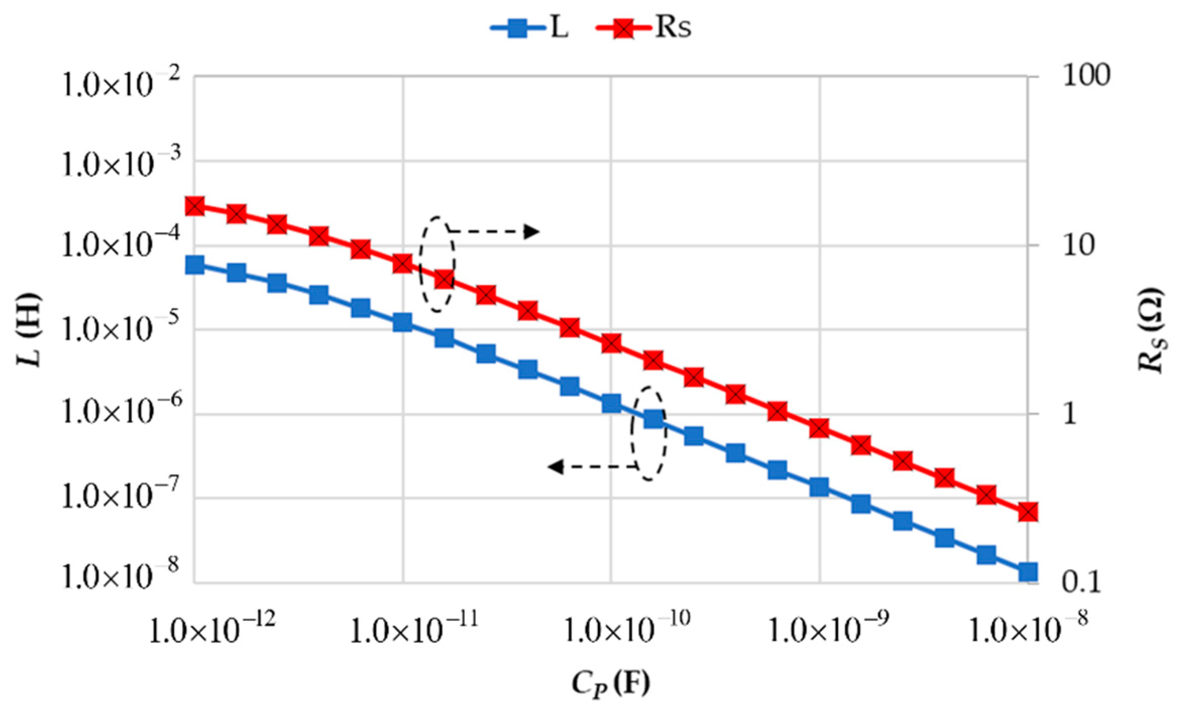
The effect of the parasitic capacitance,
CP, can be analyzed using (5). The increase of
CP occurs as the inductance value declines. From (23), the series inductor
LS proportionally influences the ESR,
RS, value. Its behavior is illustrated in
Figure 13.
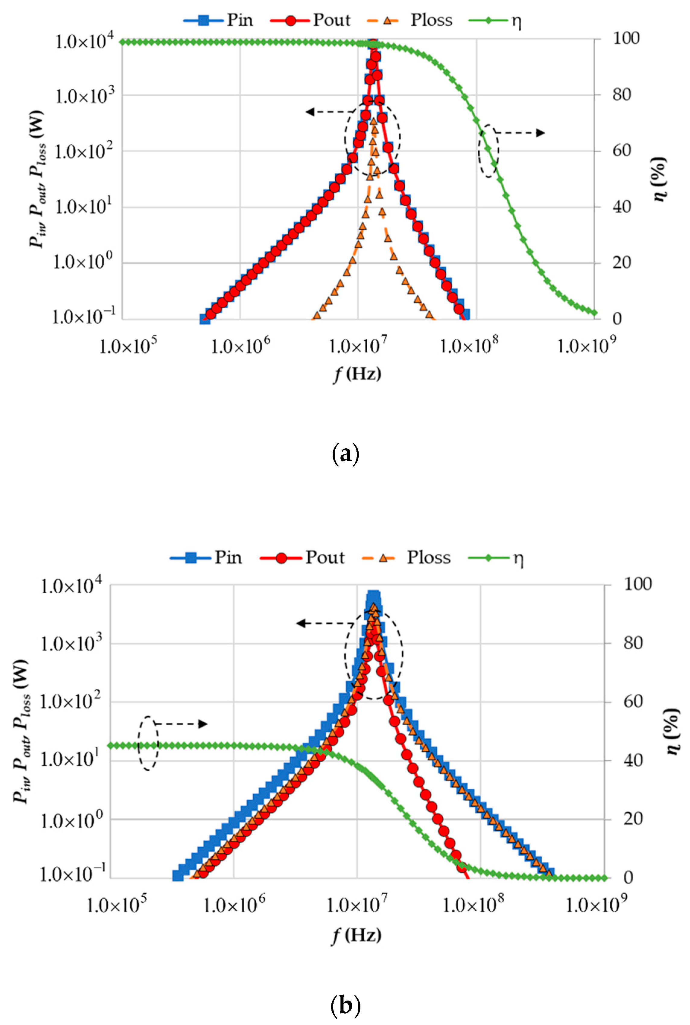
The relationship between power and efficiency with a frequency response is shown in
Figure 14. It can be seen that, by having a lower ESR value (here below 1 Ω, see
Figure 14a), less power is lost in the inductor, resulting in more power being delivered. The system may achieve an efficiency of over 95%. On the contrary, when the series resistance of the inductor is greater, it consumes some power, impacting the output power delivered to the load. From
Figure 14b, the overall efficiency can be understood to drop. Thus, to minimize the loss caused by the resonant inductor, lower values of ESR result in higher efficiencies. One way to reduce ESR is by implementing a litz wire.
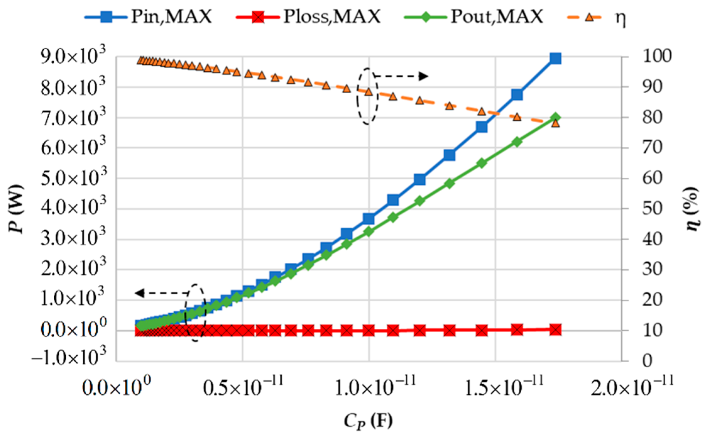
2.4. Scaling Design for Various Loads
This subsection analyzes the behavior of power and efficiency under the variation of the load resistance. The resonant-inductance parameters used in this analysis are presented in
Table 2. The ESR of the inductor,
RS, was calculated using (23). The value of inductance,
L, changes due to parasitic capacitance,
CP. Furthermore,
RS depends on its value. The parameters of the circuit model for power and efficiency analysis are listed in
Table 3.
The behavior of the load resistance to the output power for various values of parasitic capacitance is illustrated in
Figure 15a, while
Figure 15b draws the load-resistance behavior to the efficiency with the shield parasitic-capacitance variations. The escalation in the load resistance
RL from 1 Ω to 125 Ω (which amplifies
CP from 1 pF to 1 nF) results in power increases. Increasing load resistance is determined to decrease power loss in the inductor.
2.5. Scaling Design for Various Parasitic Capacitances on the Shield-Coupler Stress Voltage
To acquire a thinner module of the shielded-CPT, the space gap between the shield plate and the coupler plate should be as short as possible. By decreasing the gap, the parasitic capacitance
CP increases. Assuming no stray capacitance on the edges of the plate, it can be estimated as
where
dSC and
SP are the gap distance between the shield-coupler plates and shield plate area, respectively. From (7), let us assume that
CC is much smaller than
CP; the stress voltage behavior is inversely proportional to the amount of parasitic capacitance (see (27)). While the gap is smaller, the parasitic capacitance will become greater. Here, increasing
CP will increase the stress voltage
V1. The EF value between the shield-coupler plates,
ESC, can be calculated as follows:
From (28), the EF level is amplified in proportion to the increase in stress voltage. As we know, the EF in air has a breakdown voltage
EMAX above 30 kV/cm [
34], which is essential for system scaling. From this point, the EF strength between the shield-coupler plates should have a value under
EMAX. The effect of parasitic capacitance upon the stress voltage is shown in
Figure 16. With decrease in
dSC, the capacitance
CP increases. The stress voltage over shield-coupler plates increased, which increased the EF between them proportionally.


