Article

Voltage Transients Mitigation in the DC Distribution Network of More/All Electric Aircrafts

1
Department of Electrical and Computer Engineering, Democritus University of Thrace, Kimmeria ECE Campus, 67132 Xanthi, Greece
2
Solutions Engineering Center, ON Semiconductor, 85609 Munich, Germany
*
Author to whom correspondence should be addressed.
Energies 2020, 13(16), 4123; https://doi.org/10.3390/en13164123
Submission received: 3 July 2020 / Revised: 28 July 2020 / Accepted: 6 August 2020 / Published: 10 August 2020

Abstract

:
The objective of this paper is to present a power conversion system, based on a bidirectional DC/DC converter, along with a supercapacitor bank, that mitigates the voltage transients that occur on the DC distribution network of More/All Electric Aircrafts. These transients, such as voltage sags and swells appear on the DC buses of on-board microgrids, mainly due to load variations and are classified according to the aircrafts electric power system standards. First, we shortly describe an aircraft distribution network, that is applicable to the most common actual aircraft architectures, then we present the proposed system, along with the bidirectional DC/DC converter design, the control technique and the supercapacitor bank sizing. Finally, we present simulation and experimental results that support the effectiveness of the proposed system to effectively compensate voltage transients, supporting the DC buses in dynamic conditions. Concluding, the proposed system provides high power quality and compliance with the respective power quality standards for aircraft microgrids.

1. Introduction

Having in mind the development of more efficient and environmentally friendly aircrafts, the biggest aircraft manufacturers have started to incorporate the concept of More and All Electric Aircraft (M/A-AE). The main idea of M/A-AE technology is to use electric power for replacing other non-electric power sources, used in a conventional aircraft (e.g., hydraulic, mechanical or pneumatic). As such, the largest civil aircraft models, i.e., Airbus 380 and Boeing 787 both incorporate MEA technology. The total installed electric power of the latter one (B787) reaches up to 1 MVA, which makes it the aircraft with the highest electrification level nowadays [1,2]. Towards this direction, the Advisory Council for Aviation Research and Innovation in Europe is envisioning the incorporation of M/A-EA concept within the “Flightpath 2050” program which, among others, sets some very strict long-term environmental goals [3].
As the electrification level of large civil aircrafts is expected to increase in the near future, more electronically controlled loads are emerging. In this context, the aircraft electrical power system is of particular interest in all respects. Power converters are the key elements for efficient energy conversion in the distribution network of the aforementioned system. In more detail, bidirectional power converters constitute components of paramount importance for energy transactions either between the on-board microgrid buses, which may adopt different voltage characteristics (i.e., AC or DC, various voltage levels, various frequencies etc.), or between a bus and an energy storage system [4]. Considering the latter case, both long- and short-term energy storage units have been employed in many cases, leading so to hybrid configurations (e.g., batteries and supercapacitors) [5,6,7]. Thus, with an appropriate energy management scheme prioritizing the different energy sources, depending on the frequency content of the bus request, these systems are capable to face the challenging issues of power flow regulation, voltage stability and fast dynamic response [4], achieving high power quality for the M/A-EA microgrid.
In this paper, the power quality issues are focused, considering a DC-bus based electrical distribution system. The transient phenomena (e.g., voltage sags and swells) that may occur at the High Voltage DC (HVDC) bus of the distribution network are investigated, in order to design, construct and evaluate (through simulations and experiments) a power conversion system capable of mitigating these voltage transients. The aforementioned system comprises a bidirectional DC/DC converter, a supercapacitor bank and an appropriate control scheme. In contrast to the aforementioned works [5,6,7] that focus on a general energy management scheme, in this paper we focus on the compensation of voltage transients and as such, our system operates solely during voltage sags or swells. Hence, the primary goal of the proposed system is to provide voltage support during dynamic conditions, in order to cope with the respective power quality standards.

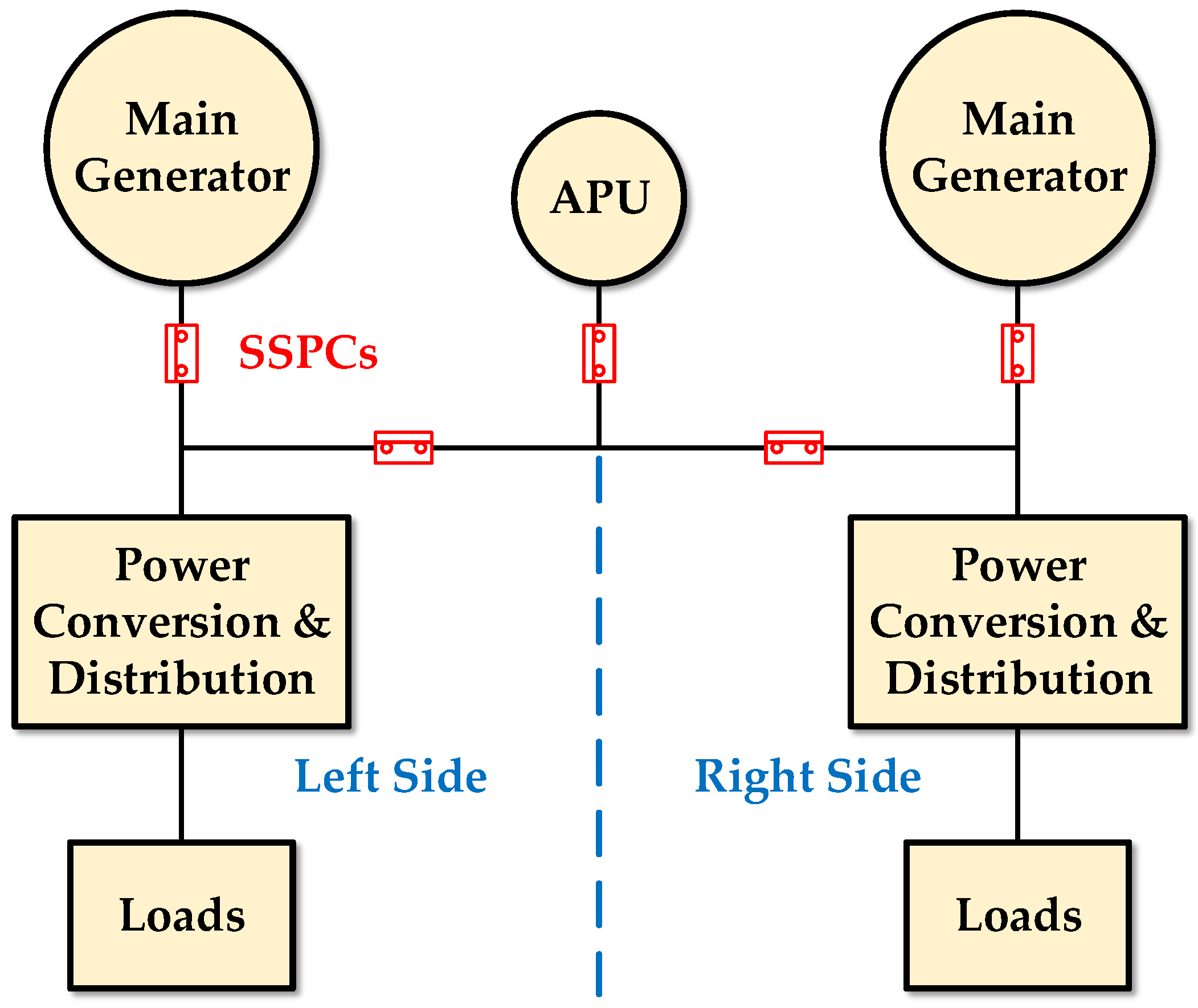
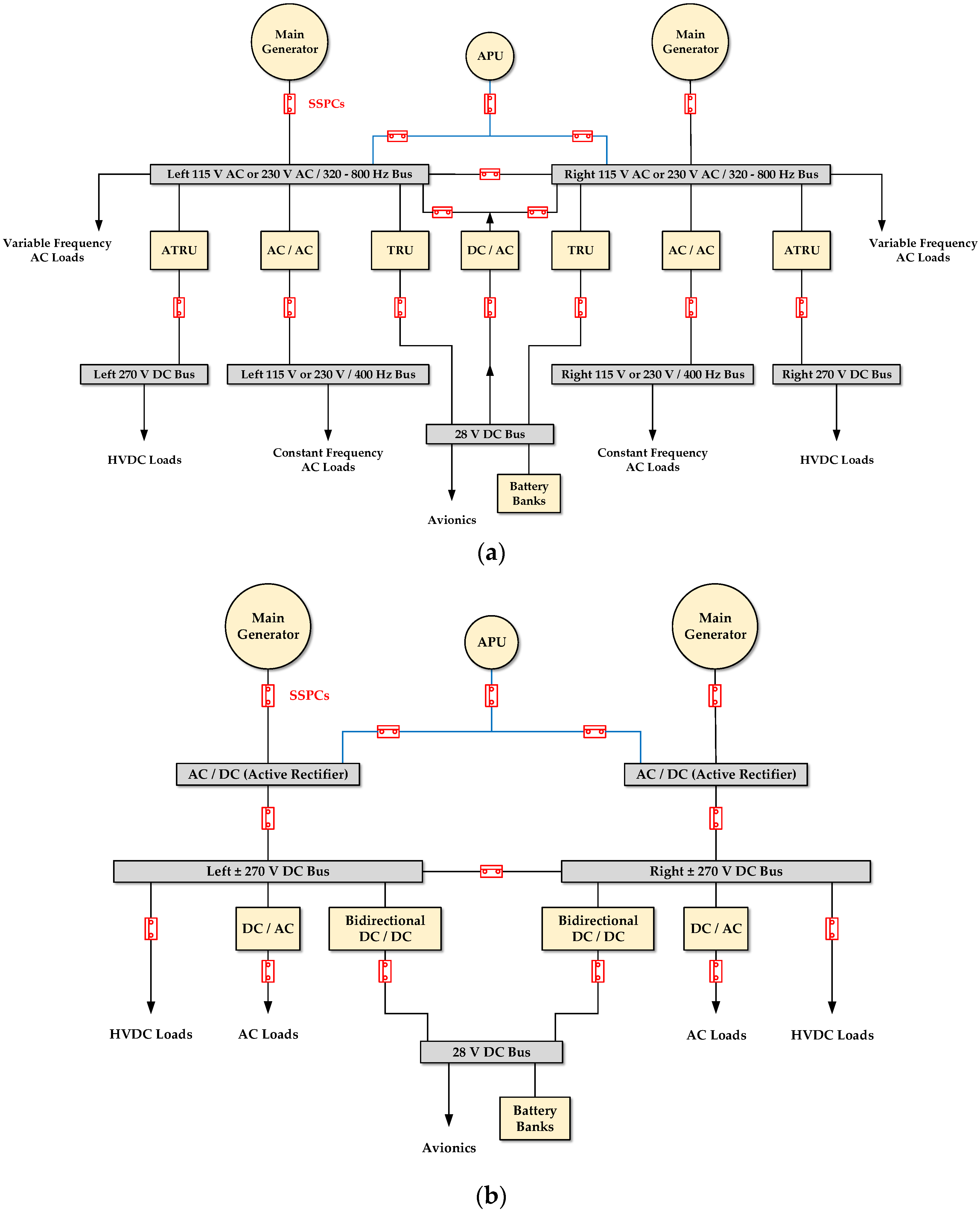
2. More/All Electric Aircraft System Description

The basic power system architecture of an aircraft is presented in Figure 1, where the main generators and auxiliary power units (APUs) are depicted, along with the power conversion and distribution system, the loads and the Solid State Power Controllers (SSPCs).
In general, there are two main generator units in an aircraft. Those are driven by combustion engines or by auxiliary power units, when the airplane is landed (Figure 1). The electric power that is generated is converted and then distributed via the distribution network of the aircraft. The main distribution system architectures, appropriate for the M/A-EA concept are described in the next subsection.

2.1. General Description

Regarding the distribution network architecture, the constant frequency AC distribution (115 V/400 Hz) has been commonly used in conventional commercial aircrafts (e.g., A320, B737). It consists of 115 V AC and 28 V DC buses, whereas 400 Hz constant frequency is achieved by means of a constant speed drive [8].
However, the latest aircraft models (e.g., A380, B787) incorporate a hybrid AC and DC distribution architecture with 115 V/360–800 Hz or 230 V/360–800 Hz AC and 270 V or 540 V (±270 V) DC. In this architecture, the heavy and inefficient constant speed drive is removed and the generator is directly connected to the engine, leading to variable frequency of the primary AC bus. Currently, this distribution architecture is considered a suitable platform for future aircrafts [9].
Additionally, a purely HVDC distribution architecture has been proposed, utilizing 270 V or 540 V (±270 V) DC buses. This architecture is a very promising solution for future M/A-EAs and has been investigated in the context of several research projects, such as Clean Sky JU [10] and MOET EU [11]. This distribution network configuration comes also as a consequence of the emerging technology of DC microgrids [12,13,14]. Both the aforementioned a) hybrid and b) purely HVDC distribution network configurations are depicted in Figure 2, where TRU stands for Transformer Rectifier Unit, whereas ATRU stands for Auto-Transformer Rectifier Unit.
The advantages of DC distribution systems, compared to their AC counterparts have been extensively presented in the scientific literature over the past few years, including higher efficiency and reliability with simpler control schemes. Furthermore, modern power systems, such as the M/A-EA distribution network, feature various electronic loads, energy storage systems and distributed power units, which are in their vast majority DC or (at least) adopt an intermediate DC-link, leading so to DC distribution architectures [12,13,14,15,16].
It is worth noting that the voltage transients mitigation system that we propose is based on a DC/DC converter, and thus it can be effectively integrated in both of the abovementioned distribution network architectures (which are dominant for future M/A-EAs), as they both incorporate a DC distribution network. Figure 3 depicts the incorporation of the proposed system into the DC distribution network of a M/A-EA, with hybrid or purely HVDC configuration.

2.2. Voltage Transients

As the electrification level of civil aircrafts is constantly increasing, load variations and intermittent operation may lead to transient phenomena and voltage disturbances which impact the DC voltage of the distribution network buses [17].
In general, a DC voltage transient usually occurs either because of normal disturbances, such as electric load steps and engine speed changes, or because of a momentary power interruption and an abnormal disturbance, such as a fault clearing. According to MIL-STD-704F [18], which is the standard for aircraft electric power characteristics, transients are classified into three categories, namely lesser, normal and abnormal transients. Lesser transients are those that do not exceed the steady state limits. Normal transients may exceed the steady state limits but they remain within the specified normal transient region. Finally, transients that exceed normal transient limits (as a result of an abnormal disturbance) and eventually return to steady state limits are defined as abnormal transients.
In this work, the proposed system aims to mitigate voltage sags and swells that occur as a result of abnormal transients, mainly because of load step changes. To do so, we propose the utilization of a DC/DC converter, along with a supercapacitor bank, to be connected to the main HVDC bus. Finally, it is worth noting that the proposed concept can be also applied in the DC network of electric vehicles or in any other DC network, the voltage level of which needs to be maintained within strict limits.

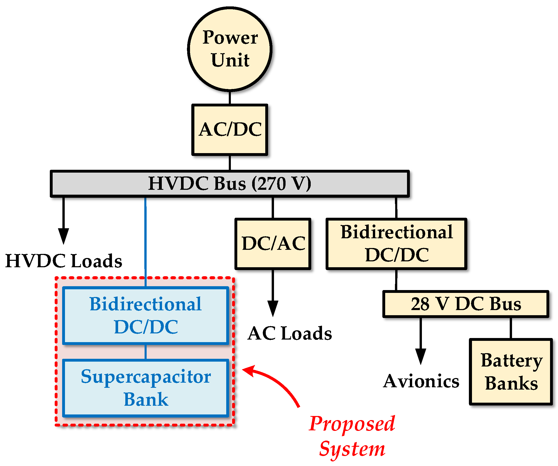
3. Proposed System Description

In order to compensate the above described voltage transients, we propose a power conversion system comprising a bidirectional converter, based on the Bidirectional Buck-Boost Converter (BBBC) topology, along with a supercapacitor bank. The main components of the proposed system, for both power and control stages are described in the following subsections. Furthermore, we propose a design for hardware implementation.

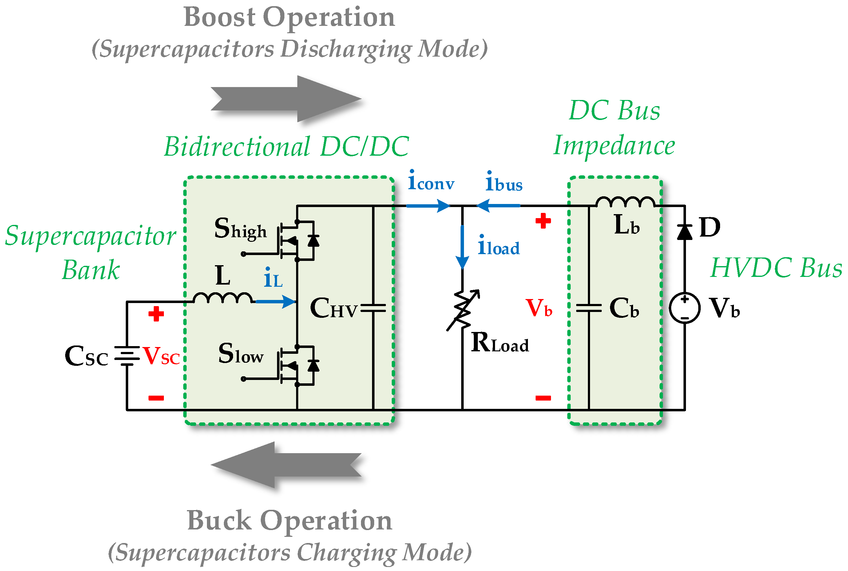
3.1. Bidirectional Buck-Boost Converter

The DC/DC converter is the core component of the proposed compensation system and plays a vital role for the realization of the proposed concept, as it acts as the interface between the supercapacitor bank and the HVDC bus. In this regard, the BBBC topology consists a well-established DC/DC architecture and seems to be in favor for energy recovery (e.g., regenerative braking for electrical machines) and active power filtering applications, as well as various two-quadrant applications, where bidirectional power flow is imperative [19,20]. Moreover, it incorporates a minimum number of semiconductor switches and passive components.
The BBBC power stage is depicted in the schematic diagram of Figure 4. It consists of a semiconductor switches pair (power MOSFETs) in half-bridge configuration and an inductor connected at the bridge-leg common point. The high voltage side is connected to the HVDC bus, whereas the low voltage side is connected to the supercapacitor bank; supercapacitor technology provides ultra-high energy storage capability at low rated voltages [21]. In our application, the Silicon Carbide (SiC) power MOSFETs NVHL160N120SC1, provided by ON Semiconductor® are used. The proposed SiC switches accommodate the hard-switching behavior of the converter without requiring any heatsink or forced air cooling. As such, compact designs with very high power densities are possible. Two modes of operation are considered, according to the schematic diagram of Figure 4, namely buck or step-down (power flows from high to low voltage side—supercapacitors are charging) and boost or step-up operation (power flows from low to high voltage side—supercapacitors are discharging). In both cases, synchronous operation can be supported, because of the half-bridge configuration of the topology. If synchronous operation is not desired, then the antiparallel diode of the inactive switch operates as a freewheeling diode [22].
In addition, the converter may operate either in Continuous Conduction Mode (CCM), or in Discontinuous Conduction Mode (DCM), depending on the inductor current. CCM operation results in less current ripple, hence less magnetic and turn-off losses. On the other hand, DCM operation results in increased current ripple, and hence higher magnetic, conduction and turn-off losses [21,23]. However, DCM operation requires smaller inductance value and offers faster dynamics because of the cycle-by-cycle current regulation.
In this work CCM operation along with a current controller is selected, achieving both low current ripple (thus reduced losses) and fast dynamic response. The CCM operation is designed for a wide range of operation, by properly selecting the inductance value (L) and the switching frequency (fs) of the converter. The necessary internal current control loop is based on the Peak Current Control (PCC) method and it is digitally implemented with the aid of a microcontroller unit [22,24,25,26].
Finally, the driver FAN7390 by ON Semiconductor has been selected for the converter driving circuit. This driver is an excellent and cost-effective solution for the current application and it is based on the well-established bootstrap supply technique (its operating principle is described in detail in [26]). For the bootstrap driver diode, we have used the RHRD660S from ON Semiconductor, making the DC/DC converter system a complete ON Semiconductor solution.

3.2. Supercapacitor Bank

As for the energy storage systems, supercapacitors and battery banks are usually employed for this kind of applications. As regards the power and energy density and life time, these two energy storage technologies are characterized by opposite features [21]. Hence, in various applications they are combined, adopting so hybrid energy storage configurations.
Compared to batteries, supercapacitors provide high capacitance, higher power density, lower energy density and longer life time [21]. Owing to their aforementioned characteristics, supercapacitors are able to compensate steep voltage transients and effectively support the DC bus.
For this work, a supercapacitor bank of approximately 12.92 F is utilized, comprising 24 series connected supercapacitors with a capacitance and maximum voltage values of 310 F and 2.7 V, respectively. As it will be shown later on, the capacity of 12.92 F is overwhelming for the experimental DC/DC converter design of this paper. This capacity corresponds to much higher power rating converters that we are planning to construct in the near future. For the needs of this paper, however, we used an experimental prototype which is just a scaled-down version of the final one, focusing more on the validation of the voltage sag/swell mitigation concept, and not so much on the converter and system design.

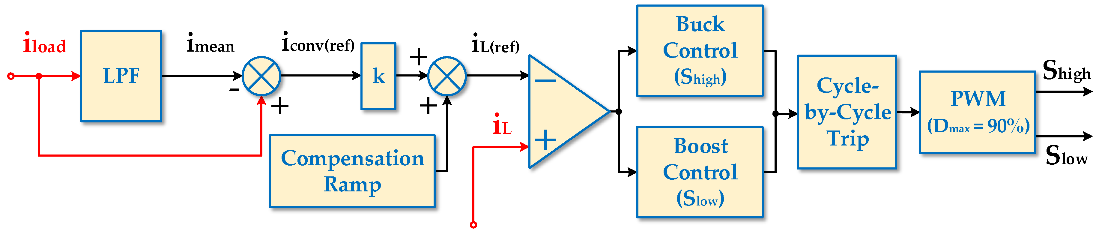
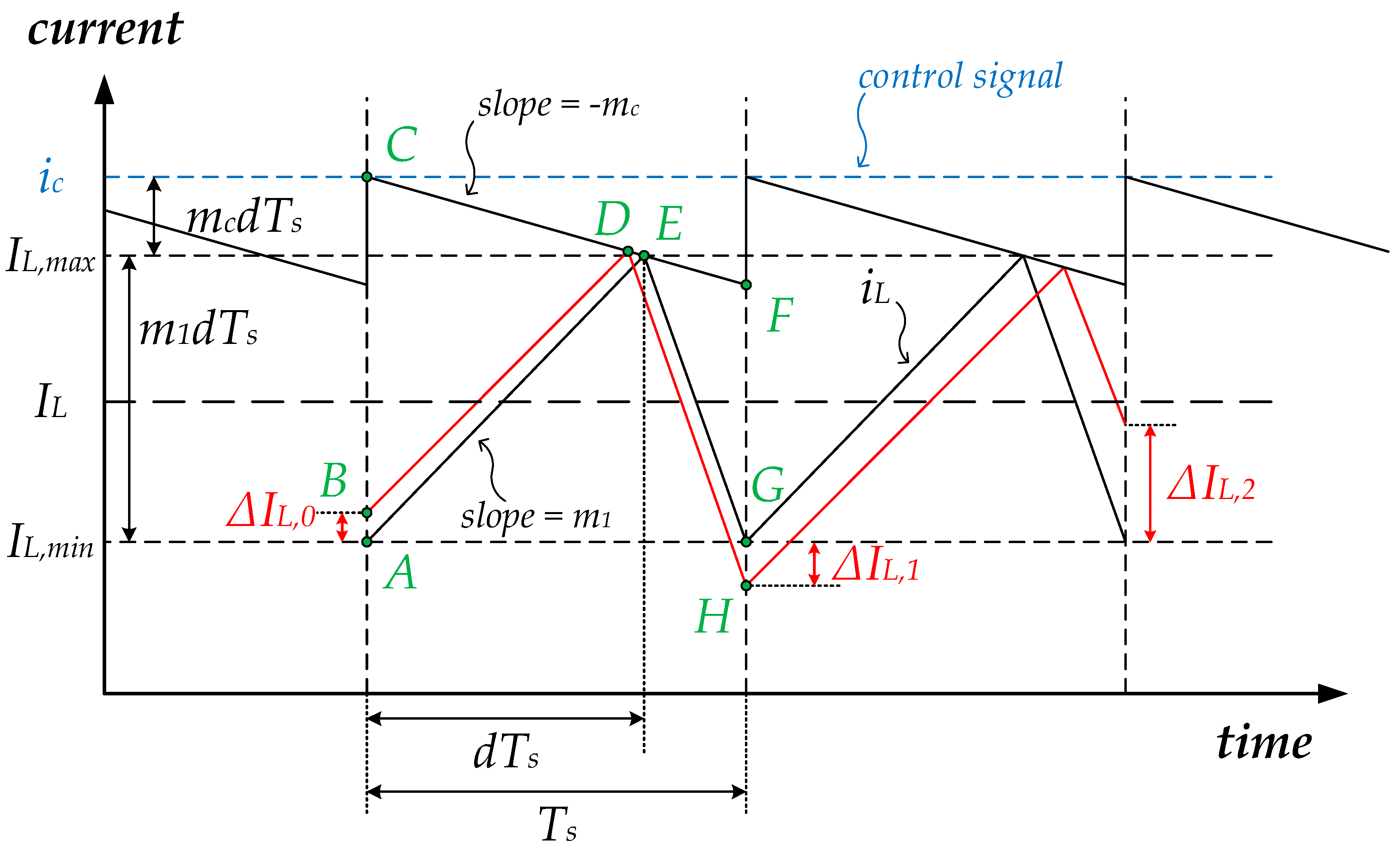
3.3. Control Technique

As regards the control scheme, it is based on the load current monitoring and the decoupling of its high-frequency component via a digitally implemented Low-Pass Filter (LPF), so as the proposed converter to operate solely during voltage transients. In order to identify the voltage transient, given the fact that the real-time DC bus generator current is an unavailable parameter, the load current measurement is used. The high-frequency current component is decoupled from the mean value, by means of the LPF. The cutoff frequency (fc), which is a parameter of major importance for the design of the control scheme, depends on the time constants of the DC bus generator (i.e., electrical and mechanical characteristics), which are modeled via an equivalent impedance for the DC bus. Thus, the appropriate fc values may be effectively determined via simulations for the proposed system. Three values are finally selected (1 Hz, 2 Hz and 5 Hz), and the system dynamic performance is evaluated via both simulations and experiments, in respect to the aforementioned fc values. As it will be shown later on (in Section 4), the 1 Hz value for the LPF cutoff frequency is superior to the 2 Hz and 5 Hz cases, providing effective voltage support and compliance with the MIL-STD-704F power quality characteristics. The block diagram of the proposed control scheme is given in Figure 5; k-factor is elaborated next; the compensation ramp calculation process is elaborated in Appendix A.
In more detail, for the control block diagram the power converter current reference is derived, after the subtraction of the filtered current value from the actual current value. During normal operation the result of this subtraction is approximately zero. On the other hand, during transient phenomena the output of the filter differs from the actual current value. That difference is used as the input reference current for the BBBC. During transients, the BBBC has to source (positive reference provided by the control scheme) or sink (negative reference provided by the control scheme) current during the transient state, in order to effectively mitigate the voltage transients. In other words, the BBBC has to provide the amount of current that the DC bus generators cannot support, due to their relatively slow time response constants.
Apparently, the proposed control scheme is in principal a current controller for the inductor current, based on the well-established PCC technique. In order to maintain a linear relation between the input reference current of the BBBC and its output current, the converter is designed for CCM operation with low (<5%) inductor current ripple. In that way, the output current of the converter is linearly linked to the inductor current (in both the boost and the buck mode) by the factor of the input/output voltages ratio. In more detail, considering steady state operation and CCM, the transfer functions for boost (1) and buck (2) modes are given below [27]:
V H I G H V L O W = 1 1 d ,
V L O W V H I G H = d ,
where d stands for the duty ratio of the converter primary switch (in each case), whereas VHIGH and VLOW refer to the average voltage values, for the high voltage and low voltage side, respectively. The converter may operate either in buck mode or in boost mode, thus the terms “input” and “output” are not preferred here, as they may be confusing. Assuming zero power losses (i.e., ideal components) and that the switching period (Ts) is much smaller than the disturbance time interval (i.e., transient due to load step change), it can be assumed that:
P H I G H = P L O W ,
V H I G H · I H I G H = V L O W · I L O W ,
where PHIGH, PLOW and IHIGH, ILOW are the power and current average values over a switching cycle, referring to the high and low voltage side respectively. Rearranging (4), it is easy to acquire:
V H I G H V L O W = I L O W I H I G H .
However, according to Figure 4, the average value of the low side current (ILOW) equals to the average value of the inductor current (IL). In addition, in cases of low current ripple, the peak inductor current is almost equal to the mean value. Thus, the following expression is derived:
V H I G H V L O W = I L I H I G H .
Hence, for both boost and buck modes, the mean value of the inductor current is calculated, as:
I L = ( V H I G H V L O W ) I H I G H .
And thus:
k = V H I G H V L O W .
As such, it should be noted that the reference current that is generated by the aforementioned subtraction has to be firstly multiplied by the converter ratio (k) and then to be used as the inductor current reference for the BBBC. A more detailed description of PCC is given in the following paragraph.
The principle of PCC is based on the determination of the on-time interval of the primary converter switch, by the rise of the inductor current up to its predetermined reference peak value. As for the advantages of this method, the inherent fault protection, due to the limit in the inductor peak current value, as well as the fast-dynamic response and relatively simple feedback compensation (in case of an outer control loop), make PCC one of the most popular solutions for DC/DC conversion applications. In addition, the adoption of synchronous rectification operation, (which may increase the overall converter efficiency) is feasible, whereas filter design for the input and the output stages becomes simpler, due to the constant switching frequency that PCC employs. On the other hand, the drawback of subharmonic oscillations is common in both step-up and step-down DC/DC converters operating in CCM under current-mode control. However, these oscillations are successfully damped with the addition of a compensation ramp (which is actually a saw-tooth waveform with negative slope), with properly calculated slope, to the control signal [22]. The procedure of the slope calculation for a properly designed compensation ramp is presented in detail in Appendix A.
The above control concept is digitally implemented with the aid of a microcontroller, whereas it is noted that a higher-level control loop is also applied. This high-level controller is a supervisor, responsible for the energy management of the supercapacitors. It supervises the charge level and regulates the bidirectional converter to charge/discharge them accordingly. Eventually, the energy management scheme task is to maintain the supercapacitors voltage within a predefined region, so as the converter to effectively operate in both boost and buck modes and effectively mitigate both voltage sags and swells.

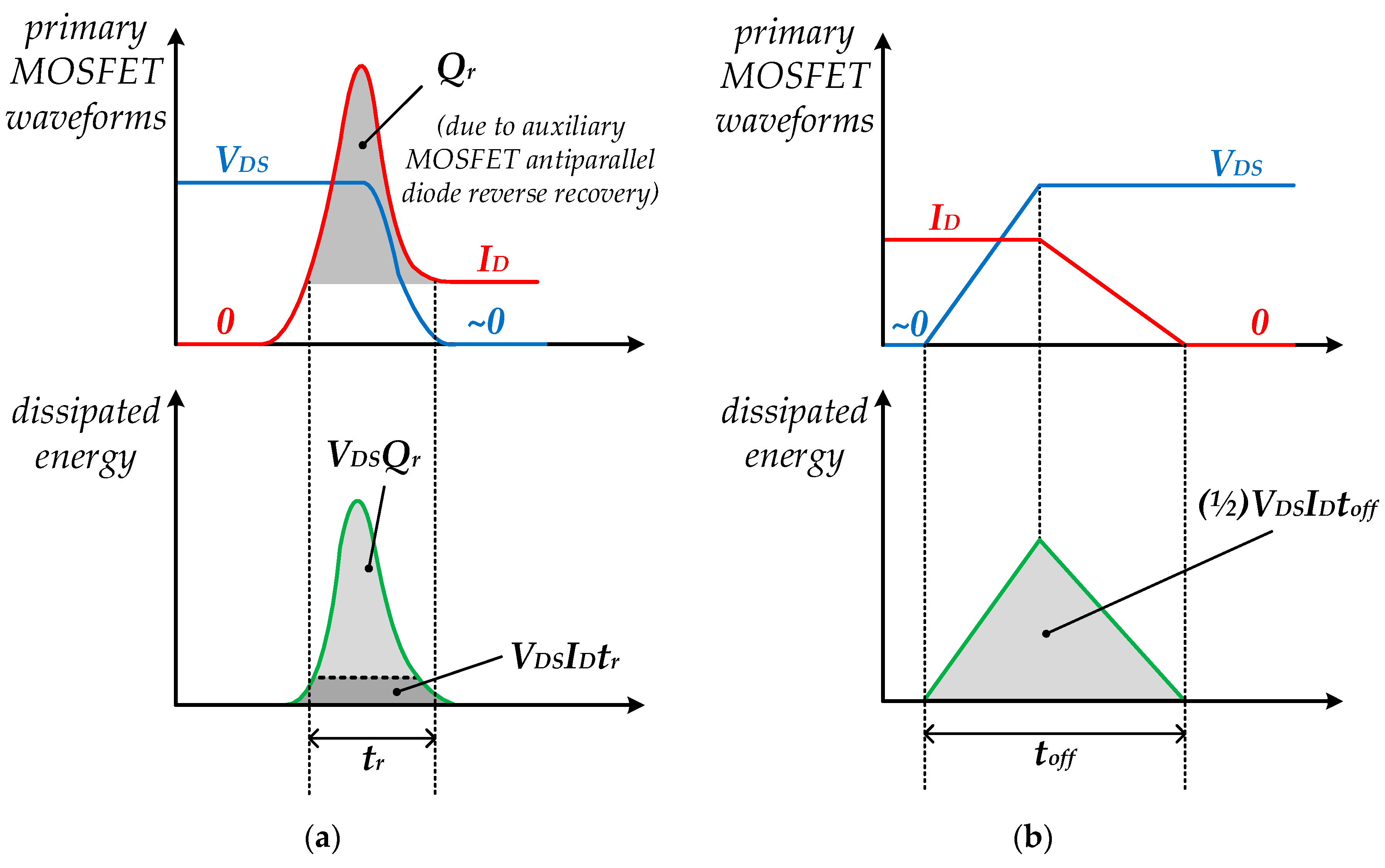
3.4. Power Losses Analysis

In order to estimate the energy losses as accurately as possible, during the operation of the proposed system, a power losses analysis is performed in this subsection. The total power losses (Plosses) are distinguished into three individual terms, that is the supercapacitor bank losses (Pscaps), i.e., conduction losses coming from the supercapacitors ESR (Equivalent Series Resistance), the BBBC inductor copper losses (Pind) and the semiconductor losses (Psemi), i.e., power losses (both conduction and switching) coming from the BBBC semiconductor switches [23]. It is noted that the inductor ferrite core magnetic losses are omitted, as they constitute a minimum amount of the total power losses, in our application, due to the limited high frequency current ripple.
Hence, the expression for the power losses is given in Equation (9):
P l o s s e s = P s c a p s + P i n d + P s e m i .
As regards the supercapacitors and the inductor power losses, it is obtained:
P s c a p s = i L , r m s 2 · R s c a p s ,
P i n d = i L , r m s 2 · R L ,
where Rscaps is the supercapacitors ESR value, RL is the inductor parasitic resistance, and iL,rms is the RMS (Root Mean Square) value of the inductor current, which flows through the supercapacitors as well, as they are connected to the low voltage side (Figure 4).
As for the semiconductor switches (SiC power MOSFETs) losses, these are divided into two components, i.e., the conduction losses (Pcond) and the switching losses (Psw), which are calculated individually. Regarding the conduction losses, both the primary (i.e., Shigh for buck operation or Slow for boost operation) MOSFET losses and the conduction losses from the antiparallel diode of the auxiliary (i.e., Slow for buck operation or Shigh for boost operation) MOSFET are included. Hence, it is acquired:
P s e m i = P c o n d + P s w ,
P s w = P t u r n o n + P t u r n o f f .
According to [23], the conduction losses can be expressed as:
P c o n d = ( I D , r m s 2 · R D S ( o n ) ) + [ I D · Δ V o n · ( 1 d ) ] = ( I D d ) 2 · R D S ( o n ) + [ I D · Δ V o n · ( 1 d ) ] = I D [ ( I D · R D S ( o n ) · d ) + Δ V o n · ( 1 d ) ] ,
where ID equals to the MOSFET current during its on-time interval, RDS(on) is the drain-source on-resistance, ΔVon is the voltage drop of the MOSFET antiparallel diode during its conduction and d stands for the duty ratio. The drain-source resistance value depends on the gate-source driving voltage (i.e., 15 V in this application) and it has been calculated according to the SiC MOSFET datasheet [28].
As for the switching losses, they are calculated separately for the MOSFET turn-on and turn-off transitions (Equation (13)); the turn-on losses include both the controlled (primary) MOSFET losses and the antiparallel diode of the auxiliary switch losses, owing to the reverse recovery phenomenon [23]. In other words, the diode stored charge induces additional transistor switching losses, as it is depicted in Figure 6. It is noted that in our application, non-synchronous operation is considered. The amount of the recovered stored charge (Qr), which is used in the following Equations (15) and (19), can be defined as the integral of the antiparallel diode current over the tr time interval, which corresponds to the duration of the reverse recovery process [23] and it is available in the NVHL160N120SC1 SiC MOSFET datasheet [28].
According to [23] and the qualitative representation of switches transitions in Figure 6, the energy being dissipated during the turn-on transition is calculated as:
E o n = V D S · I D · t r + V D S · Q r + 1 4 V D S · Q r ,
where VDS is the MOSFET (drain-source) voltage during its off-time interval, whereas tr is the duration of the turn-on transition. It is also noted that the amount ( 1 / 4 ) · V D S · Q r corresponds to the diode switching losses. Hence, it is obtained:
P t u r n o n = E o n · f s ,
where fs represents the switching frequency.
For the turn-off transition, the calculation mechanism is similar, although without the reverse recovery losses. The dissipated energy can be calculated similarly, in respect to Figure 6, as:
E o f f = 1 2 · V D S · I D · t o f f ,
where toff is the duration of the turn-off transition. Hence, it is derived:
P t u r n o f f = E o f f · f s .
It is worth noting that the voltage and current rise/fall times are calculated according to the MOSFET rise, fall and delay times [28], in order to obtain tr and toff time intervals. Finally, by substituting Equations (10), (11), (14), (16) and (18) into Equation (9), the total power losses are obtained:
P l o s s e s = i L , r m s 2 ( R s c a p s + R L ) + I D [ ( I D · R D S ( o n ) · d ) + Δ V o n · ( 1 d ) ] + [ V D S I D ( t r + t o f f 2 ) + 5 4 V D S Q r ] f s .
As current and voltage waveforms change rapidly (as it will be shown in the following section) during the operation of the proposed system, it is reasonable for the system energy losses to be calculated with the aid of simulations. As such, taking into account all the aforementioned parameters, the SiC MOSFET datasheet and the components actual values (which are presented in Table 1), the energy losses are estimated via simulations; results are presented in the following section. It is noted that the energy losses and system efficiency have been calculated in boost mode of operation of the BBBC (voltage sag case), considering the worst-case scenario of no compensation ramp (equivalent to zero slope value, meaning that the subharmonic oscillations remain), which leads to a constant peak current reference, at its maximum value. In parallel, the impact of the LPF cutoff frequency selection is evaluated, by presenting energy losses for various fc values.

3.5. Proposed System Design

The proposed BBBC system is designed in Altium Designer® software. The foremost components used in the constructed experimental prototype, the digital controller, as well as the system parameters are summarized in Table 1. The experimental test bench is based on the schematic diagram of Figure 4.
As the constructed converter is a scaled-down version of the one that would be used on the actual DC distribution network of an aircraft, the DC bus voltage level of the converter is selected to be 120 V. Also, the DC bus impedance value has been properly scaled down, in order to effectively implement the desired voltage transients with lower current values, compared to the ones found in an actual M/A-EA system. The impedance calculation is based on various previous works that take into account the equivalent impedance of the generators, the TRUs, and the cables [32,33,34,35,36]. Finally, the initial voltage level of the supercapacitor bank is chosen to be 50 V. As it was mentioned earlier, the chosen capacity is overwhelming for the specific test bench, as it reflects a much higher support-BBBC design. Based on simulation and experimental results, the voltage drop/raise of the supercapacitor-bank during the voltage support operation of the system is less than 1 V, indicating that the chosen capacity is not optimal for the current test bench. Nevertheless, with the selected initial supercapacitors voltage (i.e., 50 V) the proposed system is able to effectively compensate both voltage sags and swells, operating in both boost and buck mode, respectively.

4. Simulation and Experimental Verification

In order the functionality and the effective voltage transient mitigation of the above described system to be validated, simulations and experiments have been performed. In this section, simulation and experimental results are presented.

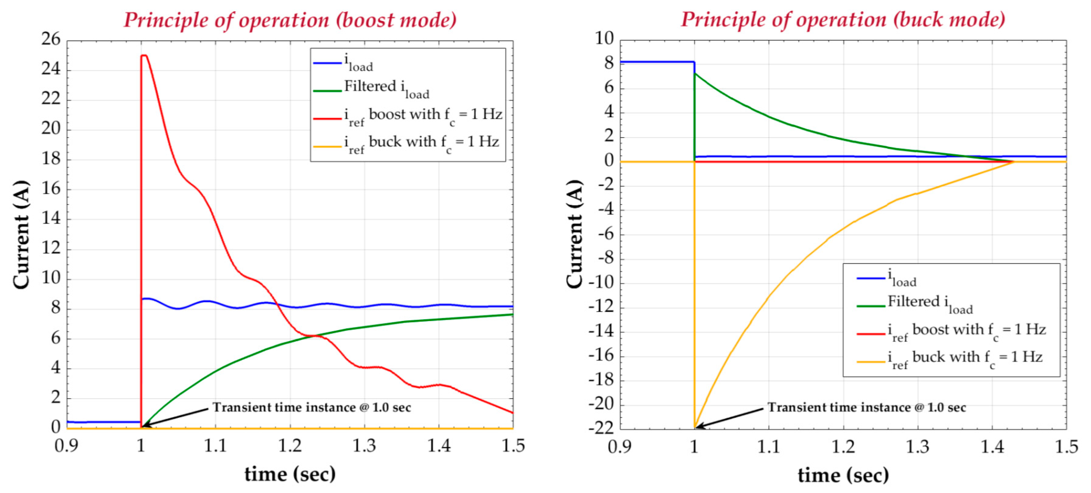
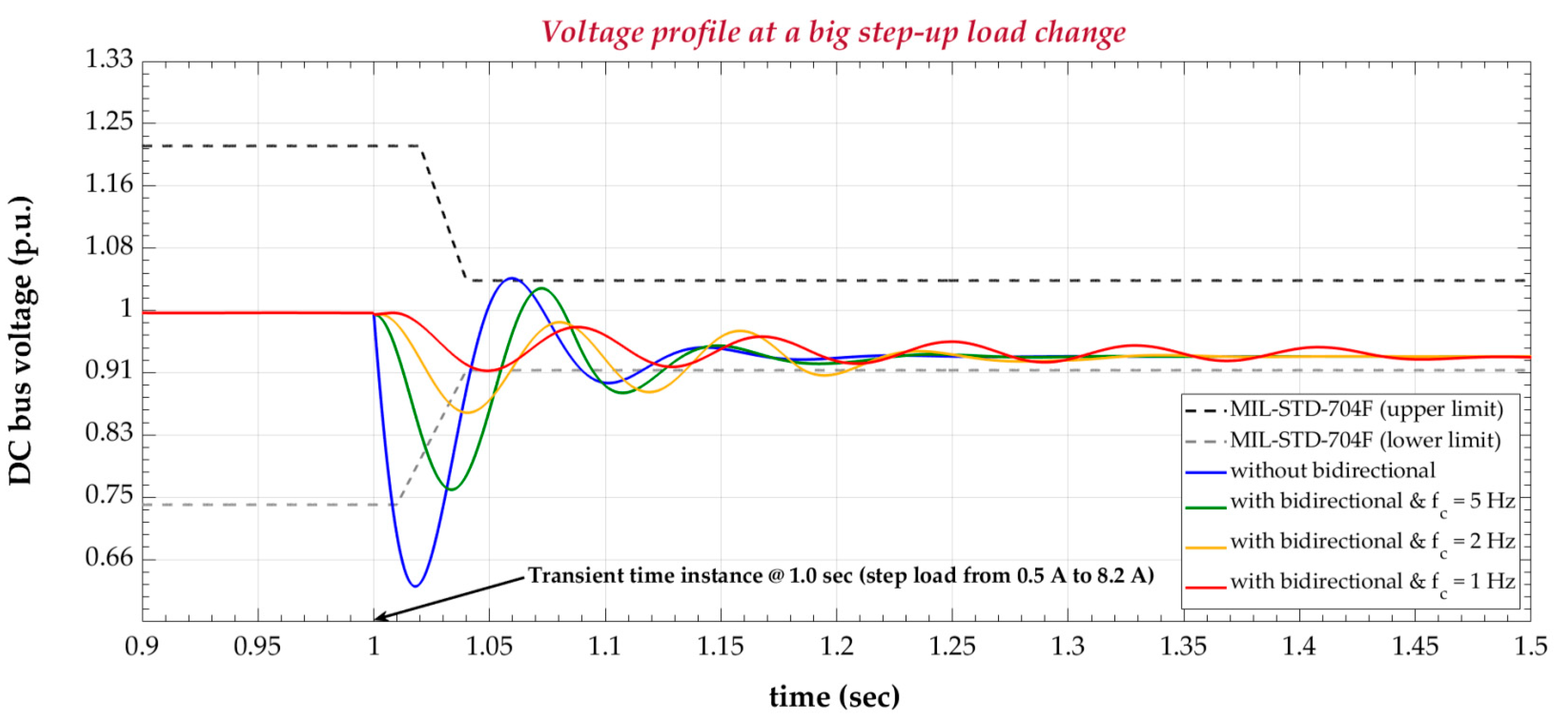
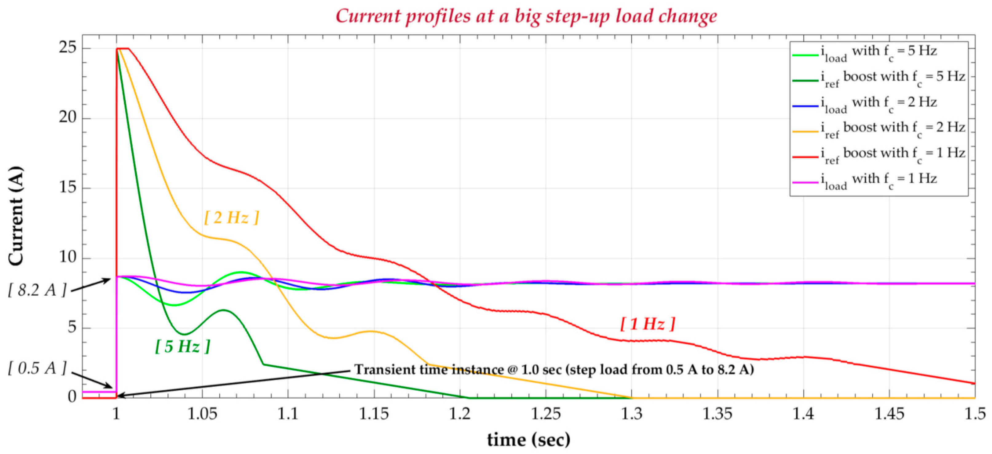
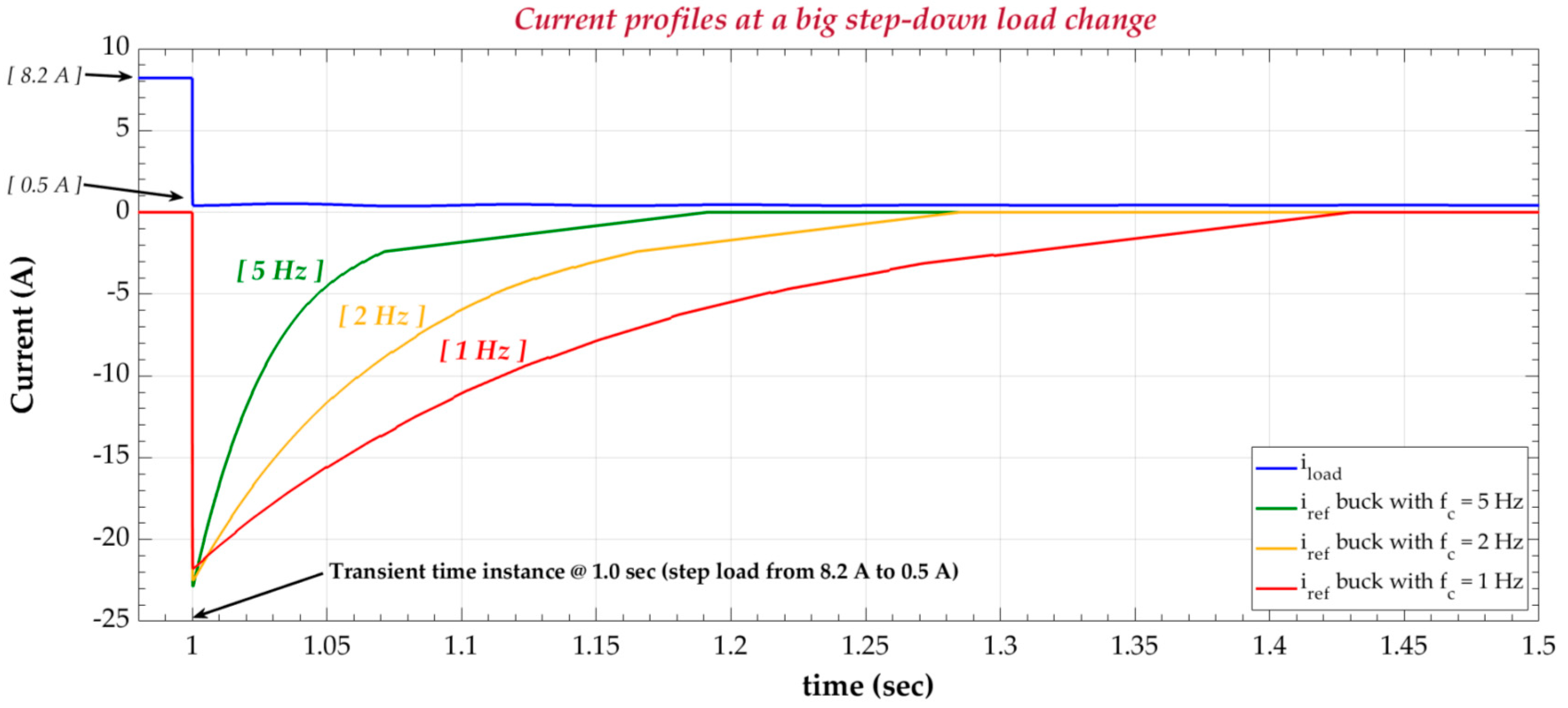
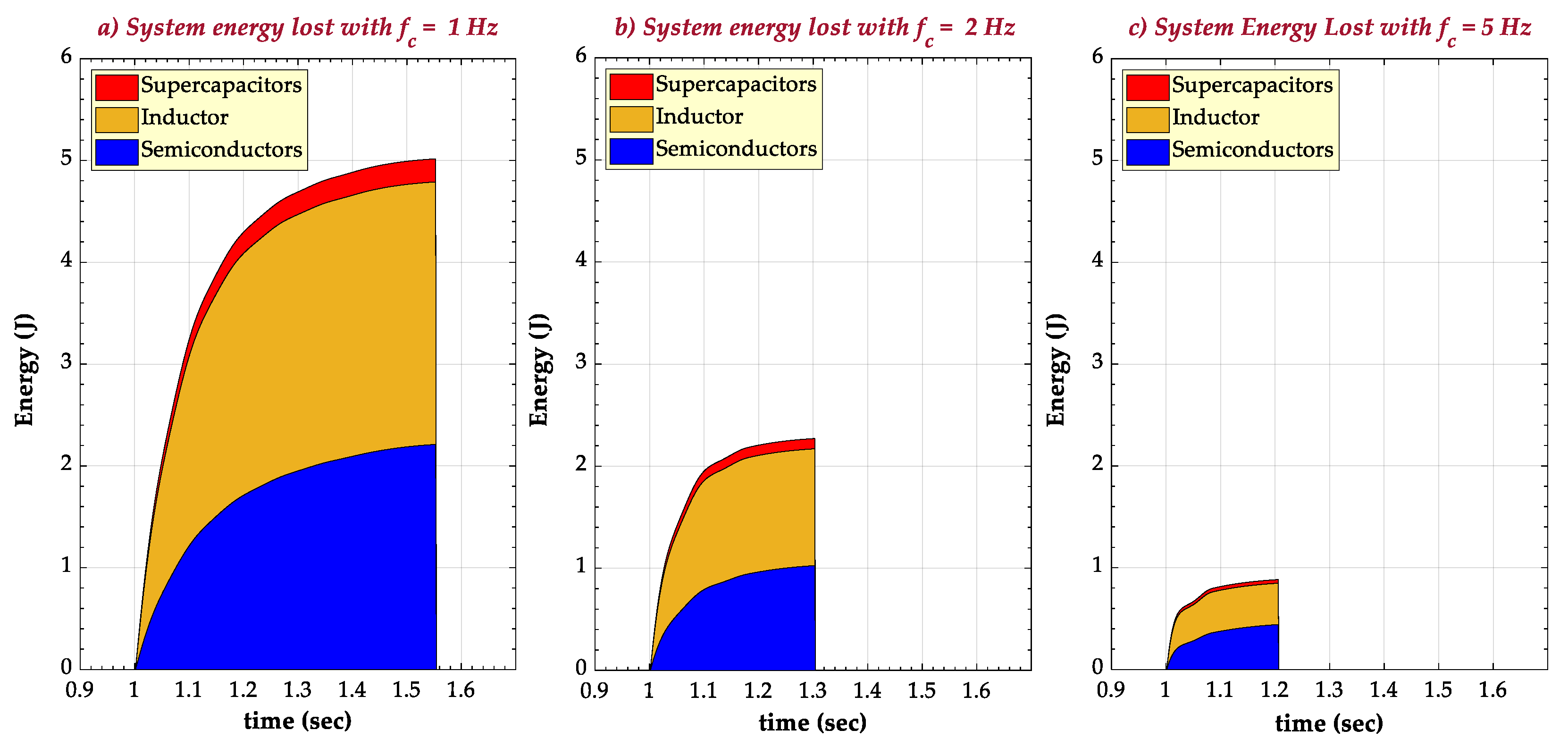
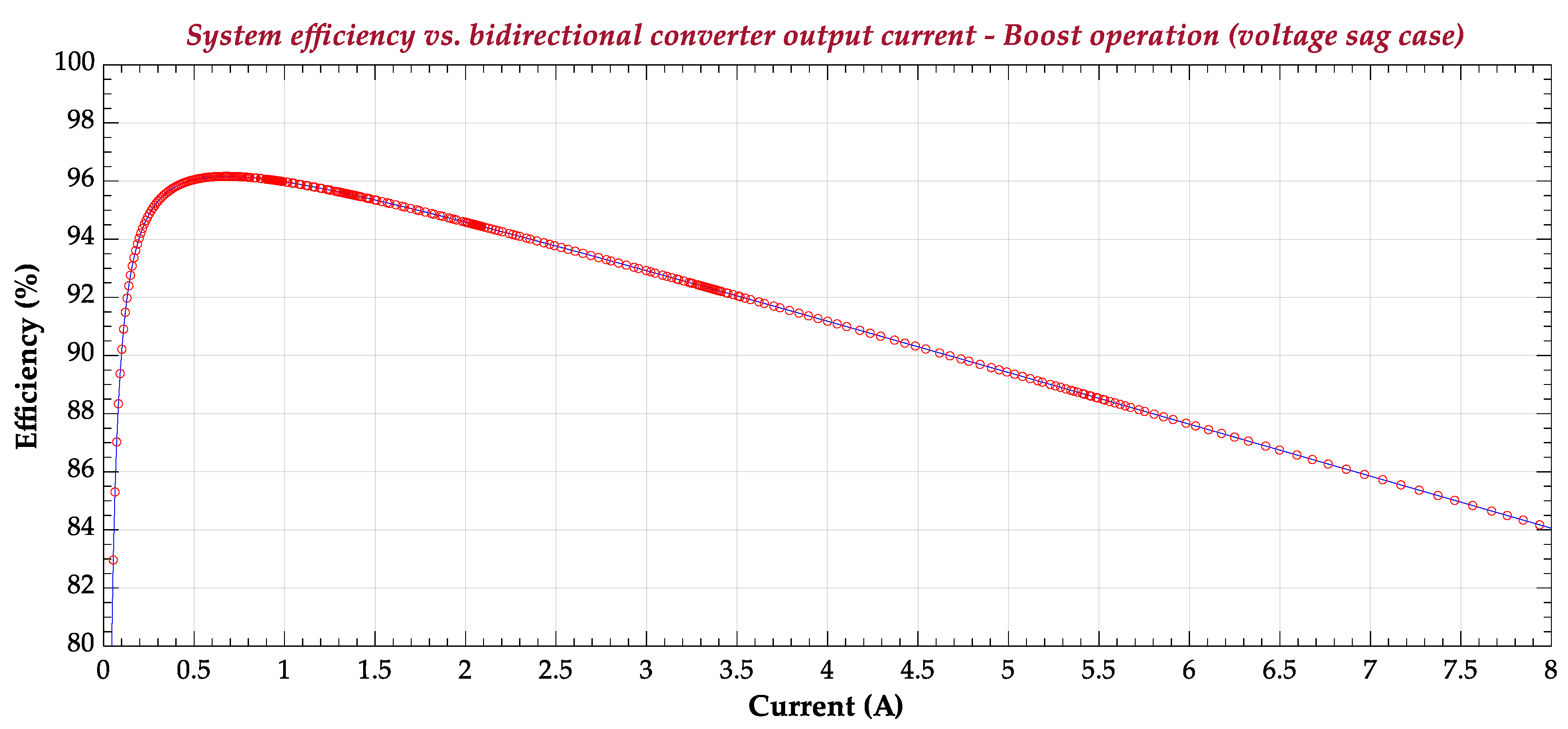
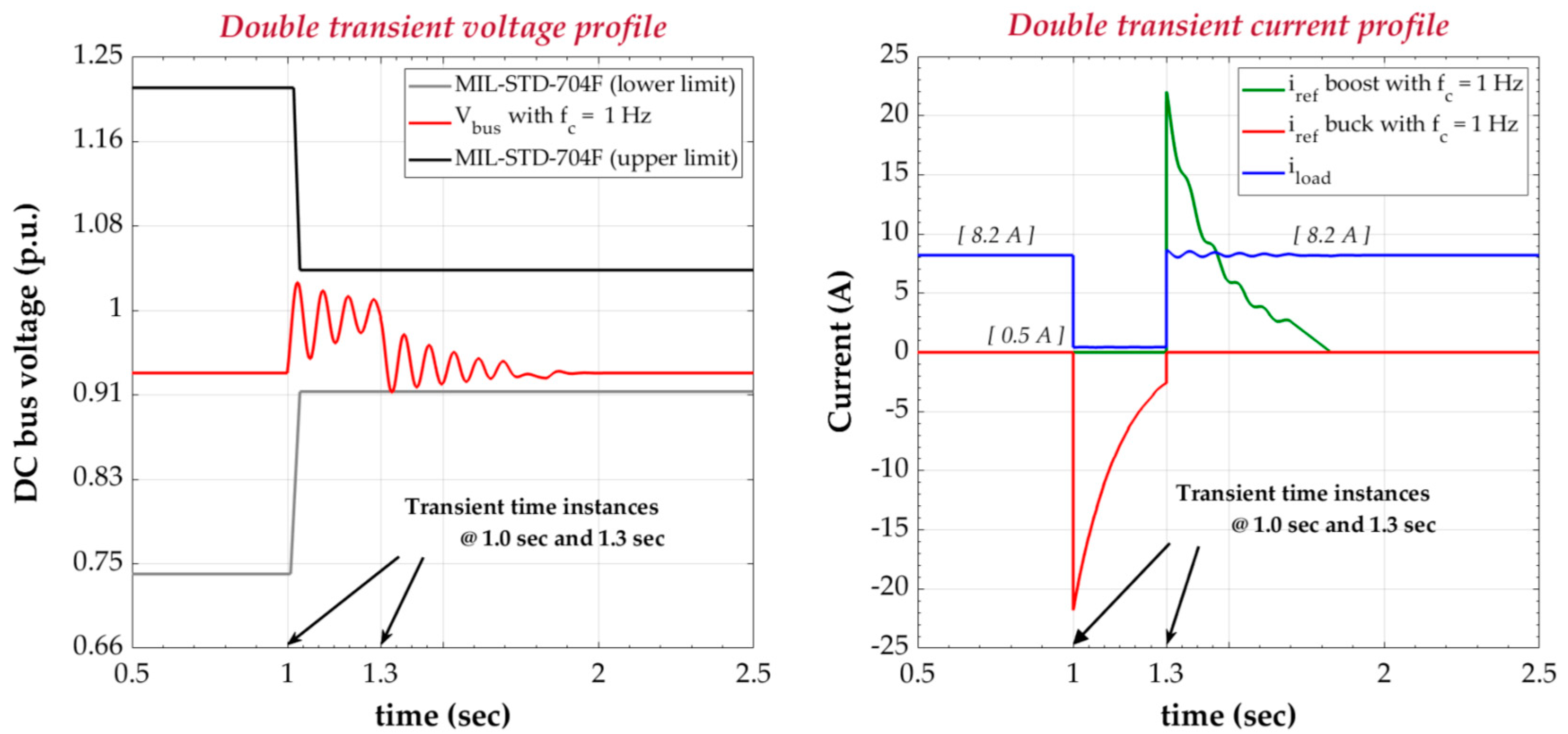
4.1. Simulation Results

Regarding the simulations, a model of the proposed system is developed via MATLAB®/Simulink® software package, which is based on the schematic diagram of Figure 4 and the parameters of Table 1. Firstly, in Figure 7, the operating principle of the BBBC is explained, for both boost (in case of voltage sag) and buck (in case of voltage swell) modes, where the load current (before and after the LPF, with the cutoff frequency fc at 1 Hz) is depicted, along with the derived BBBC current reference.
In boost mode the current reference is assumed positive, whereas in buck mode negative. Finally, a step in load is considered at 1 s, for each simulation case. For a voltage sag, the load changes from 0.5 A to 8.2 A, and vice-versa for a voltage swell.
In Figure 8 and Figure 9 the DC bus voltage profile is given, for both a voltage sag (forcing the BBBC in boost mode) and a voltage swell (forcing the BBBC in buck mode), occurring after the load step change. A comparison of the DC bus voltage profile for three different cutoff frequency values for the LPF of the controller of Figure 4 (i.e., 1 Hz, 2 Hz and 5 Hz) is also presented.
Based on the presented results we can conclude that the BBBC operation with 1 Hz LPF cutoff frequency mitigates the voltage transients sufficiently (for both buck and boost operation), maintaining the bus voltage within the region for normal transients, defined in MIL-STD-704F standard. The load current and the BBBC inductor reference current with the LPF cutoff frequency as a parameter are depicted in Figure 10 and Figure 11, for the voltage sag and voltage swell test case, respectively.
The inductor current (as well as the total converter current reference) is inversely proportional to the LPF cutoff frequency, implying that a cutoff frequency of fc = 1 Hz will force the BBBC to operate for a longer duration, as such providing more energy to the DC bus, with respect to the fc = 2 Hz and fc = 5 Hz, accordingly. Hence, the lower the LPF cutoff frequency, the higher the total energy losses of the system are, as it is presented in Figure 12. In more detail, the total amount of energy losses is approximately 5 J, for the case of fc = 1 Hz, whereas this amount is decreased by 54.7% and by 82.4%, for the cases of fc = 2 Hz and fc = 5 Hz, respectively. In parallel, both the inductor and semiconductor switches losses play a major role to the total amount of the system power losses, with a percentage of approximately 50% for the inductor and 46% for the MOSFETs power losses, while the rest (4%) portion, corresponds to the supercapacitor bank conduction losses.
It is worth noting that the energy losses have been calculated in boost mode of operation of the BBBC (voltage sag case), considering the analysis presented in Section 3.4, in respect to the datasheet parameters [28], without the addition of compensation ramp (worst-case scenario). The estimated efficiency of the system in boost operation (voltage sag case) as a function of the BBBC output current is depicted in Figure 13.
Finally, Figure 14 indicates the effective voltage compensation and compliance with the MIL-STD-704F normal voltage transient limits in the worst-case scenario of a double transient condition, where a voltage swell is followed by a voltage sag, occurring at 1 s and 1.3 s, respectively. Both DC bus voltage and current profiles are depicted.

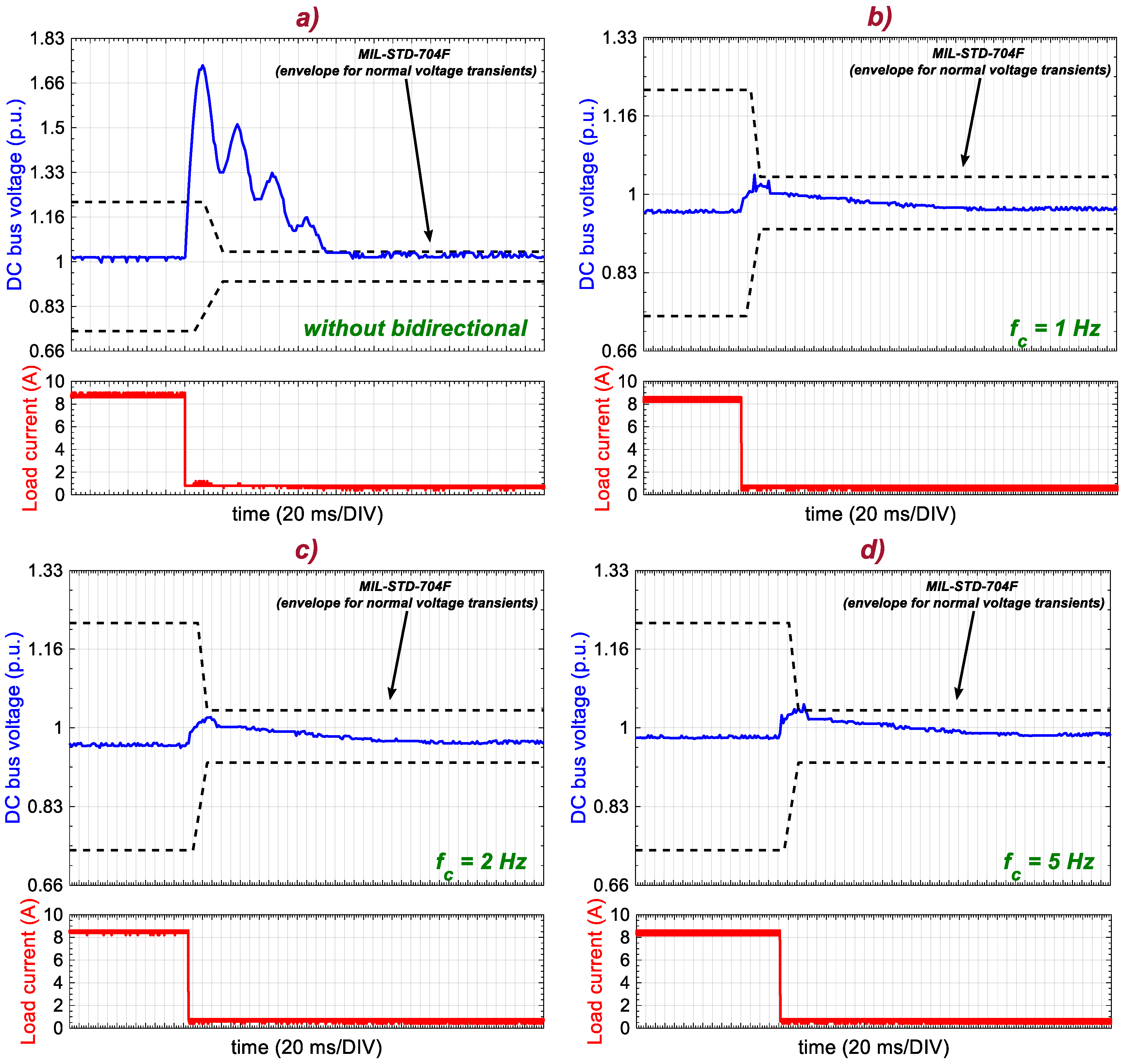
4.2. Experimental Results

Experiments on a laboratory test bench have been carried out for the same load steps that have been considered in the simulations subsection, evaluating the impact of the LPF cutoff frequency as well, in order to experimentally investigate the proposed system performance. Indicative results are provided in Figure 15 and Figure 16.
Specifically, the DC bus voltage profile is shown in Figure 15, during a voltage sag (caused by a load step increase), considering a LPF cutoff frequency of 1 Hz, 2 Hz and 5 Hz. In Figure 16 the DC bus voltage profile is depicted, over a voltage swell (caused by a load step decrease), along with the respective fc values. Finally, for comparison purposes, the DC bus voltage response without the proposed system is included both in Figure 15 and Figure 16.
Based on the experimental results presented in Figure 15 and Figure 16, we conclude that the BBBC operation with fc = 1 Hz is superior to the 2 Hz and 5 Hz operation (confirming so the simulation results), and that it may effectively mitigate voltage transients, supporting the DC bus voltage, in order to remain within the defined envelope for normal transients, according to MIL-STD-704F.

5. Conclusions

In this work a power conversion system is presented, aiming to effectively mitigate voltage transients that occur on the DC bus of an on-board distribution network. The proposed system comprises a bidirectional converter (BBBC) and a supercapacitor bank, along with a PCC-based controller and a supervisor to implement the proposed concept. The foremost circuitries of the converter, being the power stage SiC switches and the driving circuit are both implemented with ON Semiconductor parts.
The DC bus voltage profile improvement that can be achieved with the proposed system in cases of voltage transients, has been verified through both simulation and experimental results. Last but not least, keeping the DC bus voltage within the normal transient limits highlights the MIL-STD-704F standard compliance that can be achieved with the aid of the proposed system. To conclude, this work as a whole aims to contribute to the challenging issue of voltage compensation techniques and power quality maintenance, concerning the on-board microgrids of M/A-EAs, which will be the dominant technology for future civil aircrafts.

Author Contributions

Conceptualization, N.R. and N.P.; methodology, N.R., D.V., T.J. and N.P.; software, N.R. and D.V.; validation, N.R., D.V., T.J. and N.P.; formal analysis, N.R., D.V., T.J. and N.P.; investigation, N.R., D.V. and T.J.; resources, N.R., D.V. and T.J.; data curation, N.R. and D.V.; writing—original draft preparation, N.R.; writing—review and editing, N.R., D.V., T.J. and N.P.; visualization, N.R.; supervision, N.P.; All authors have read and agreed to the published version of the manuscript.

Funding

This research received no external funding.

Acknowledgments

The authors would like to acknowledge the support of ON Semiconductor for providing the semiconductor switches and all required drivers and ICs for the hardware implementation of the proposed solution.

Conflicts of Interest

The authors declare no conflict of interest.

Nomenclature

Abbreviations
ACAlternating Current
APUAuxiliary Power Unit
ATRUAuto-Transformer Rectifier Unit
BBBCBidirectional Buck-Boost Converter
CCMContinuous Conduction Mode
DCDirect Current
DCMDiscontinuous Conduction Mode
ESREquivalent Series Resistance
HVDCHigh Voltage Direct Current
M/A-EAMore/All Electric Aircraft
MEAMore Electric Aircraft
MOSFETMetal Oxide Semiconductor Field Effect Transistor
PCCPeak Current Control
PWMPulse Width Modulation
RMSRoot Mean Square
SiCSilicon Carbide
SSPCSolid State Power Controller
TRUTransformer Rectifier Unit
Symbols
CbDC bus capacitance
CHVBidirectional converter high voltage side capacitance
CSCSupercapacitor bank capacitance
dBidirectional converter duty ratio
EoffEnergy dissipated during turn-off transition
EonEnergy dissipated during turn-on transition
fsBidirectional converter switching frequency
ibusDC bus current (supplied to load)
icControl signal (peak current reference)
iconvBidirectional converter current (source/sink to/from the DC bus)
IDAverage value of the MOSFET drain current
ID,rmsRMS value of the MOSFET drain current
IHIGHAverage value of the bidirectional converter high voltage side current
ILAverage value of the inductor current
IL,maxMaximum value of the inductor current
IL,minMinimum value of the inductor current
IL,rmsRMS value of the inductor current
iloadLoad current
ILOWAverage value of the bidirectional converter low voltage side current
kCurrent reference multiplication factor (bidirectional converter gain)
LBidirectional converter inductance
LbDC bus inductance
m1Rising slope of the inductor current
mcCompensation ramp slope
PcondMOSFET conduction power losses
PHIGHAverage power at the bidirectional converter high voltage side
PindInductor conduction power losses
PlossesTotal system power losses
PLOWAverage power at the bidirectional converter low voltage side
PscapsSupercapacitor bank conduction power losses
PsemiMOSFET power losses
PswMOSFET switching power losses
Pturn-offSwitching power losses during turn-off transition
Pturn-onSwitching power losses during turn-on transition
QrRecovered stored charge of the antiparallel diode
RbDC bus resistance
RDS(on)MOSFET drain-source on-resistance
RLResistance of the bidirectional converter inductor
RLoadLoad resistance
RscapsSupercapacitor bank resistance
ShighUpper bidirectional converter MOSFET (controlled in buck mode)
SlowLower bidirectional converter MOSFET (controlled in boost mode)
toffTurn-off transition time interval
trTurn-on transition time interval
TsBidirectional converter switching period
VbDC bus voltage
VDSMOSFET drain-source voltage
VHIGHAverage voltage at the bidirectional converter high voltage side
VLOWAverage voltage at the bidirectional converter low voltage side
VscSupercapacitors voltage
Vsc(max)Supercapacitors maximum voltage
ΔILInductor current disturbance
ΔIL,0Initial (first cycle) small disturbance in the inductor current
ΔIL,1Small disturbance in the inductor current at the second switching cycle
ΔIL,2Small disturbance in the inductor current at the third switching cycle
ΔVonVoltage drop of the MOSFET antiparallel diode during its conduction

Appendix A

A schematic diagram of the PCC technique with the addition of a compensation ramp is depicted in Figure A1. It is noted that in this figure the compensation ramp slope is improperly calculated, on purpose, in order to highlight the fact that the inductor current disturbance (ΔIL) can be amplified, after a couple of switching cycles, thus the impact of the compensation ramp slope (mc) has to be verified.
Figure A1. Schematic diagram of the peak current control technique with the addition of an improperly calculated compensation ramp.
Energies 13 04123 g0a1
Assuming a small disturbance (ΔIL,0) in the inductor current, it turns out that the line segment AE is parallel to BD and respectively DH is parallel to EG, according to Figure A1. Hence, the triangle BCD is similar to ACE, whereas the triangle GFE is similar to HFD and thus it is obtained:
{ Δ I L , 0 A C = E D E C E D F D = Δ I L , 1 F G .
It is noted that the absolute value is considered, for the inductor current disturbances (ΔIL,0 and ΔIL,1) in Equation (A1). As such, it does not matter, whether the sign of the current disturbance is positive or negative. Hence it is derived:
{ E D = E C Δ I L , 0 A C E D = F D Δ I L , 1 F G .
By merging the two Equations in (A2), it is acquired:
Δ I L , 1 = E C · F G A C · F D Δ I L , 0 .
However, with the aid of Figure A1 it is easily obtained:
F G F D = d 1 d .
And thus, it is derived:
Δ I L , 1 = m 1 d T s m c ( 1 d ) T s ( m 1 + m c ) d T s · d 1 d Δ I L , 0 .
In order to avoid the subharmonic oscillations, it is required:
Δ I L , 1 Δ I L , 0 .
Substituting Equation (A5) into Equation (A6), it is obtained:
m 1 d T s m c ( 1 d ) T s ( m 1 + m c ) d T s · d 1 d 1 .
Hence, after mathematical manipulations, it is derived:
m c m 1 · 2 d 1 2 ( 1 d ) .
The slope of the compensation ramp may be set to zero (its minimum value) for d < 0.5 , whereas for d 0.5 the condition, in order to eliminate the subharmonic oscillations, is given in Equations (A9) and (A10), by substituting the slope m1 value into Equation (A8) for boost (supercapacitors discharging) and buck (supercapacitors charging) operation, respectively:
m c { 0 ,                      d < 0.5 V L O W L · 2 d 1 2 ( 1 d ) ,   d 0.5 ( Boost ) ,
m c { 0 ,                                  d < 0.5 V H I G H V L O W L · 2 d 1 2 ( 1 d ) ,   d 0.5 ( Buck ) .
Last but not least, it is worth noting that at the design stage a safety margin is usually applied by a rule of thumb (e.g., 20%) at the above slope value, so as the compensation ramp to sufficiently suppress subharmonic oscillations over a wide operating range.

References

  1. Bozhko, S.; Hill, C.I.; Yang, T. More-Electric Aircraft: Systems and Modeling. Wiley Encycl. Electr. Electron. Eng. 2018, 1–31. [Google Scholar] [CrossRef]
  2. Madonna, V.; Migliazza, P.; Giangrande, P.; Lorenzani, E.; Buticchi, G.; Galea, M. The Rebirth of the Current Source Inverter: Advantages for Aerospace Motor Design. IEEE Ind. Electron. Mag. 2019, 13, 65–76. [Google Scholar] [CrossRef]
  3. European Commission. Flightpath 2050. Europe’s Vision for Aviation. 2011. Available online: https://ec.europa.eu/transport/sites/transport/files/modes/air/doc/flightpath2050.pdf (accessed on 7 August 2020).
  4. Buticchi, G.; Costa, L.; Lissere, M. Improving System Efficiency for the More Electric Aircraft: A Look at dc/dc Converters for the Avionic Onboard dc Microgrid. IEEE Ind. Electron. Mag. 2017, 11, 26–36. [Google Scholar] [CrossRef]
  5. Buticchi, G.; Costa, L.F.; Barater, D.; Lissere, M.; Amarillo, E.D. A Quadruple Active Bridge Converter for the Storage Integration on the More Electric Aircraft. IEEE Trans. Power Electron. 2018, 33, 8174–8186. [Google Scholar] [CrossRef] [Green Version]
  6. Chen, J.; Song, Q.; Yin, S.; Chen, J. On the Decentralized Energy Management Strategy for the All-Electric APU of Future More Electric Aircraft Composed of Multiple Fuel Cells and Supercapacitors. IEEE Trans. Ind. Electron. 2020, 67, 6183–6194. [Google Scholar] [CrossRef]
  7. Todd, R.; Forsyth, A.J. DC-bus power quality for aircraft power systems during generator fault conditions. IET Electr. Syst. Transp. 2011, 1, 126–135. [Google Scholar] [CrossRef] [Green Version]
  8. Chen, J.; Wang, C.; Chen, J. Investigation on the Selection of Electric Power System Architecture for Future More Electric Aircraft. IEEE Trans. Transp. Electr. 2018, 4, 563–576. [Google Scholar] [CrossRef]
  9. Sarlioglu, B.; Morris, C.T. More Electric Aircraft: Review, Challenges, and Opportunities for Commercial Transport Aircraft. IEEE Trans. Transp. Electr. 2015, 1, 54–64. [Google Scholar] [CrossRef]
  10. The Air Transport System and Clean Sky. The Hub of Europe’s Aeronautical R&T. 2004. Available online: https://www.cleansky.eu/aviation-0 (accessed on 7 August 2020).
  11. Yang, T.; Bozhko, S.; Asher, G. Application of Dynamic Phasor Concept in Modeling Aircraft Electrical Power Systems. SAE Int. J. Aerosp. 2013, 6, 38–48. [Google Scholar] [CrossRef]
  12. Dragicevic, T.; Lu, X.; Vasquez, J.C.; Guerrero, J.M. DC Microgrids—Part II: A Review of Power Architectures, Applications, and Standardization Issues. IEEE Trans. Power Electron. 2016, 31, 3528–3549. [Google Scholar] [CrossRef] [Green Version]
  13. Dragicevic, T.; Vasquez, J.C.; Guerrero, J.M.; Skrlec, D. Advanced LVDC Electrical Power Architectures and Microgrids: A step toward a new generation of power distribution networks. IEEE Electrif. Mag. 2014, 2, 54–65. [Google Scholar] [CrossRef] [Green Version]
  14. Elsayed, A.T.; Mohamed, A.A.; Mohammed, O.A. DC Microgrids and distribution systems: An overview. Electric. Power Syst. Res. 2015, 119, 407–417. [Google Scholar] [CrossRef]
  15. Baros, D.; Voglitsis, D.; Papanikolaou, N.; Kyritsis, A.; Rigogiannis, N. Wireless Power Transfer for Distributed Energy Sources Exploitation in DC Microgrids. IEEE Trans. Sustain. Energy 2019, 10, 2039–2049. [Google Scholar] [CrossRef]
  16. Kumar, D.; Zare, F.; Ghosh, A. DC Microgrid Technology: System Architectures, AC Grid Interfaces, Grounding Schemes, Power Quality, Communication Networks, Applications, and Standardizations Aspects. IEEE Access 2017, 5, 12230–12256. [Google Scholar] [CrossRef]
  17. Yang, T.; Gao, F.; Bozhko, S.; Wheeler, P. Power Electronic Systems for Aircraft. In Control of Power Electronic Converters and Systems Vol. 2, 1st ed.; Blaabjerg, F., Ed.; Academic Press: Cambridge, MA, USA, 2018; pp. 333–368. [Google Scholar] [CrossRef]
  18. Department of Defense Interface Standard, MIL-STD-704F, Aircraft Electric Power Characteristics, March 2004. Available online: http://everyspec.com/MIL-STD/MIL-STD-0700-0799/MIL-STD-704F_1083/ (accessed on 7 August 2020).
  19. Karatzaferis, I.; Tatakis, E.; Papanikolaou, N. Analysis and design of a universal energy recovery converter for use with industrial inverters. In Proceedings of the 9th International Conference on Compatibility and Power Electronics (CPE 2015), Costa da Caparica, Portugal, 24–26 June 2015. [Google Scholar] [CrossRef]
  20. Kyritsis, A.; Papanikolaou, N.; Tatakis, E. Enhanced current pulsation smoothing parallel active filter for single stage grid-connected AC-PV modules. In Proceedings of the 13th International Power Electronics and Motion Control Conference (EPE 2008), Poznan, Poland, 1–3 September 2008. [Google Scholar] [CrossRef]
  21. Karatzaferis, I.; Tatakis, E.; Papanikolaou, N. Investigation of energy savings on industrial motor drives using bidirectional converters. IEEE Access 2017, 5, 17952–17961. [Google Scholar] [CrossRef]
  22. Rigogiannis, N.; Voglitis, D.; Papanikolaou, N. Microcontroller Based Implementation of Peak Current Control Method in a Bidirectional Buck-Boost DC-DC Converter. In Proceedings of the 20th International Symposium on Electrical Apparatus and Technologies (SIELA 2018), Bourgas, Bulgaria, 3–6 June 2018. [Google Scholar] [CrossRef]
  23. Erickson, R.W.; Maksimovic, D. Fundamentals of Power Electronics, 3rd ed.; Springer Nature Switzerland AG: Cham, Switzerland, 2020. [Google Scholar] [CrossRef]
  24. Ridley, R.B. A New, Continuous-Time Model for Current-Mode Control. IEEE Trans. Power Electron. 1991, 6, 271–280. [Google Scholar] [CrossRef]
  25. Hallworth, M.; Shirsavar, S.A. Microcontroller-Based Peak Current Mode Control Using Digital Slope Compensation. IEEE Trans. Power Electron. 2012, 3340–3351. [Google Scholar] [CrossRef]
  26. Rigogiannis, N.; Baros, D.; Lempesis, E.; Ntoga, S.; Peioglou, E.; Pechlivanis, C.; Papanikolaou, N. Experimental Investigation of a Digitally Current Controlled Synchronous Buck DC/DC Converter for Microgrids Applications. In Proceedings of the 2019 Panhellenic Conference on Electronics & Telecommunications (PACET), Volos, Greece, 8–9 November 2019. [Google Scholar] [CrossRef]
  27. Mohan, N.; Undeland, T.M.; Robbins, W.P. Power Electronics: Converters, Applications and Design, 3rd ed.; Wiley: Hoboken, NJ, USA, 2002. [Google Scholar]
  28. ON Semiconductor. Datasheet: NVHL160N120SC1. Silicon Carbide N-Channel MOSFET. Available online: https://www.onsemi.com/pub/Collateral/NVHL160N120SC1-D.pdf (accessed on 7 August 2020).
  29. ON Semiconductor. Datasheet: FAN7390. High & Low Side Gate-Driver. Available online: https://www.onsemi.com/pub/Collateral/FAN7390-D.pdf (accessed on 7 August 2020).
  30. ON Semiconductor. Datasheet: RHRD660S. Hyperfast Diode. Available online: https://www.onsemi.com/pub/Collateral/RHRD660S-D.pdf (accessed on 7 August 2020).
  31. ON Semiconductor. Datasheet: 6N137M. Logic Gate Optocoupler. Available online: https://www.onsemi.com/pub/Collateral/HCPL2631M-D.pdf (accessed on 7 August 2020).
  32. Gao, F.; Bozhko, S.; Costabeber, A.; Asher, G.; Wheeler, P. Control Design and Voltage Stability Analysis of a Droop Controlled Electrical Power System for More Electric Aircraft. IEEE Trans. Ind. Electron. 2017, 64, 9271–9281. [Google Scholar] [CrossRef]
  33. Zhang, H.; Mollet, F.; Saudemont, C.; Robyns, B. Experimental Validation of Energy Storage System Management Strategies for a Local DC Distribution System for More Electric Aircraft. IEEE Trans. Ind. Electron. 2010, 57, 3905–3916. [Google Scholar] [CrossRef]
  34. Trentin, A.; Zanchetta, P.; Wheeler, P.; Clare, J. Power Conversion for a Novel AC/DC Aircraft Electrical Distribution System. IET Electr. Syst. Transp. 2014, 4, 29–37. [Google Scholar] [CrossRef]
  35. Gao, F.; Bozhko, S.; Asher, G.; Wheeler, P.; Patel, C. An Improved Voltage Compensation Approach in a Droop-Controlled DC Power System for the More Electric Aircraft. IEEE Trans. Power Electron. 2016, 31, 7369–7383. [Google Scholar] [CrossRef]
  36. Gao, F.; Bozhko, S. Modeling and Impedance Analysis of a Single DC Bus-Based Multiple Source Multiple-Load Electrical Power System. IEEE Trans. Transp. Electrif. 2016, 2, 335–346. [Google Scholar] [CrossRef] [Green Version]
Figure 1. Basic architecture of the aircraft electric power system.
Energies 13 04123 g001
Figure 2. Proposed distribution network architectures for future aircrafts; (a) hybrid AC and DC configuration, which is used in Airbus 380 and Boeing 787 and (b) purely HVDC configuration, which is proposed within the framework of Clean Sky JU [10] and MOET EU [11].
Energies 13 04123 g002
Figure 3. Incorporation of the proposed system into the HVDC bus of a M/A-EA microgrid.
Energies 13 04123 g003
Figure 4. Schematic diagram of the proposed system and the test bench, used for simulation and experimental evaluation.
Energies 13 04123 g004
Figure 5. Block diagram of the proposed control scheme.
Energies 13 04123 g005
Figure 6. Switching losses calculation; (a) turn-on transition, (b) turn-off transition.
Energies 13 04123 g006
Figure 7. Principle of operation of the proposed system, for boost and buck modes.
Energies 13 04123 g007
Figure 8. DC bus voltage response for a voltage sag, with the LPF cutoff frequency as a parameter.
Energies 13 04123 g008
Figure 9. DC bus voltage response for a voltage swell, with the LPF cutoff frequency as a parameter.
Energies 13 04123 g009
Figure 10. Load current and inductor current reference for a voltage sag case, with LPF cutoff frequency as a parameter.
Energies 13 04123 g010
Figure 11. Inductor current reference for a voltage swell case, with LPF cutoff frequency as a parameter.
Energies 13 04123 g011
Figure 12. System energy losses for LPF cutoff frequency values of (a) 1 Hz, (b) 2 Hz and (c) 5 Hz.
Energies 13 04123 g012
Figure 13. Estimated system efficiency for boost operation (voltage sag case), with the BBBC output current as a parameter.
Energies 13 04123 g013
Figure 14. DC bus voltage and current profiles for a double voltage transient.
Energies 13 04123 g014
Figure 15. DC bus voltage response for a voltage sag, with the LPF cutoff frequency as a parameter, (a) without the proposed system; (b) fc = 1 Hz; (c) fc = 2 Hz; (d) fc = 5 Hz.
Energies 13 04123 g015
Figure 16. DC bus voltage response for a voltage swell, with the LPF cutoff frequency as a parameter, (a) without the proposed system; (b) fc = 1 Hz; (c) fc = 2 Hz; (d) fc = 5 Hz.
Energies 13 04123 g016
Table 1. Main test bench components and system parameters.
Symbol—DescriptionValue—(Manufacturer)
Bidirectional Converter
fs (switching frequency)50 kHz
L (inductance)940 μH
RL (inductor parasitic resistance)540 mΩ
CHV (high-voltage side capacitance)600 μF (WÜRTH)
Converter switches (SiC power MOSFETs)NVHL160N120SC1 (ON) [28]
Driving, Sensing and Control
Bootstrap driverFAN7390 (ON) [29]
Bootstrap capacitor10 μF (YAGEO)
Bootstrap diodeRHRD660S (ON) [30]
Optocouplers6N137M (ON) [31]
Current sensorsLTS-25 NP (LEM)
Supercapacitor Bank
Csc (supercapacitors capacitance)12.92 F (MAXWELL)
Rscaps (supercapacitors ESR)52.8 mΩ
Vsc(max) (supercapacitors maximum voltage)64.8 V
DC Bus
Vb (DC bus voltage)120 V
Lb (DC bus inductance)100 mH
Rb (DC bus resistance)900 mΩ
Cb (DC bus capacitance)1.1 mF (KEMET)

