1. Introduction
The insertion of renewable generation in the electrical grid arises some problems related to the undetermined availability of these sources [
1]. In this sense, the energy mix must be planned and diversified to improve the reliability and resilience of the electrical system. The integration of energy storage systems (ESSs) is shown as an option to allow greater penetration of renewable generation [
1,
2,
3,
4,
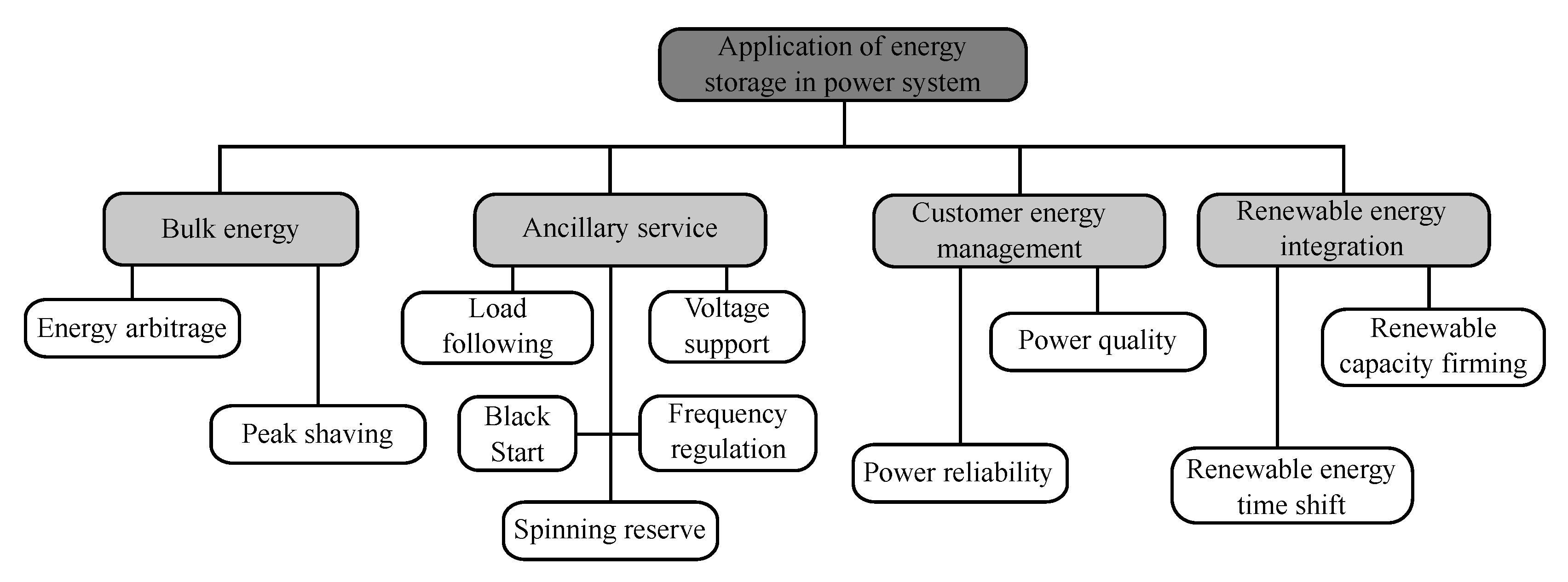
5]. Furthermore, the integration of ESSs in the power grid allows the addition of auxiliary services and increases the possibilities of power dispatch, as illustrated in
Figure 1, which provides an overview of the main functions of the ESS.
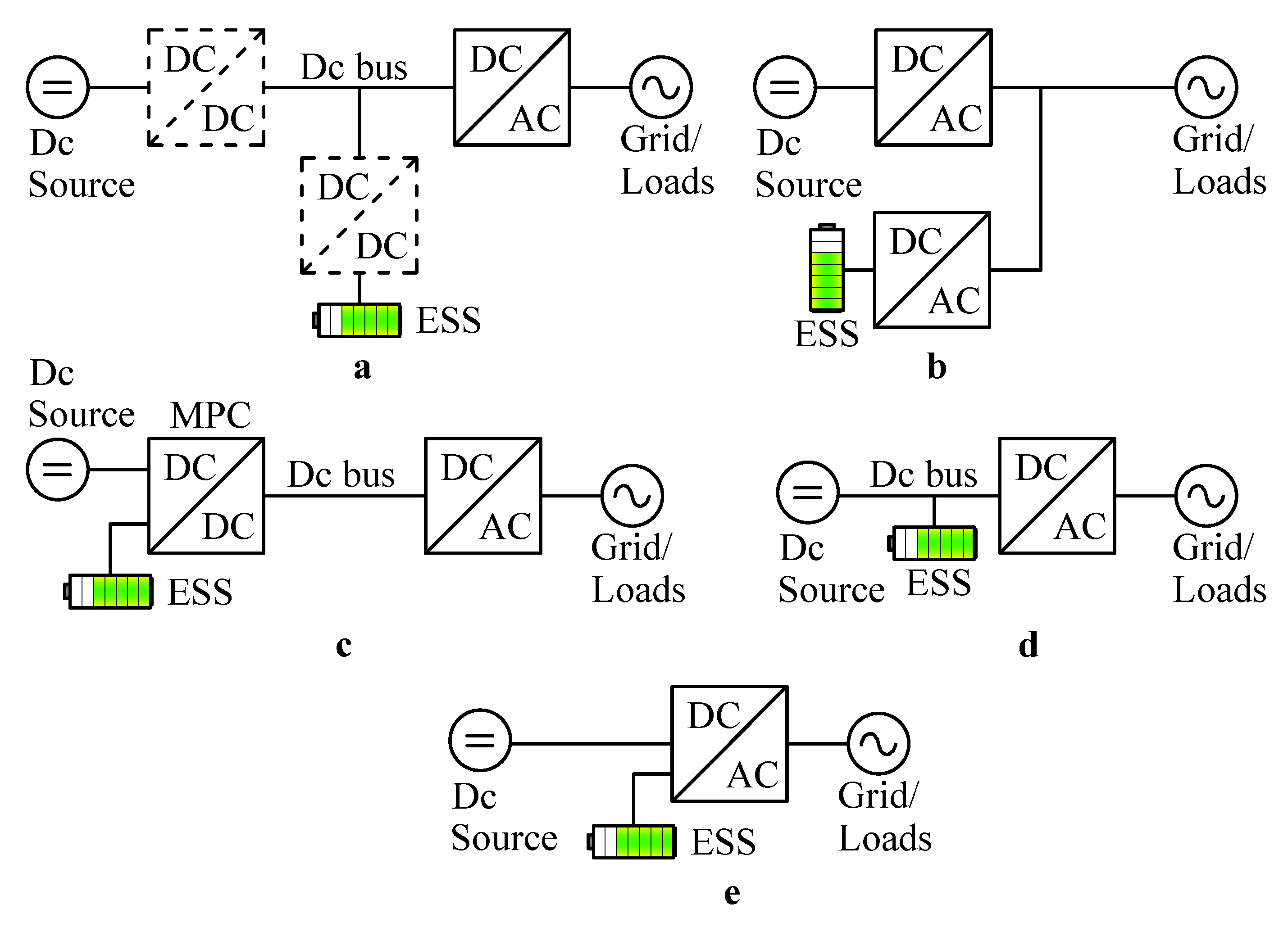
Considering an electrical system with distributed generation (DG), the connection of a renewable energy source integrated with an ESS can be performed in different ways as presented in
Figure 2. Each connection type might be interesting for a certain ESS power and/or voltage range. Besides, the design requirements and the technology of the storage system have a significant impact on the choice of the connection type.
The most used types for ESS connection are shown in
Figure 2a [
7,
8] and
Figure 2b [
9,
10]. The static converters allow bidirectional power flow for ESS charge and discharge, adapting the voltage and current at the connection point. In general, these forms of connection have a larger number of converters (and power elements) but they give the greatest design flexibility–choice of topology, voltage and current levels, passive filters, and so forth. The connection type shown in
Figure 2c uses multiport DC-DC converters (MPC) [
11]. They are particularly interesting for low power applications (<1 kW). In
Figure 2d the ESS is connected directly to the DC bus of the power inverter [
12,
13,
14]. As the main advantage, this form of connection allows the use of a single DC-AC converter to process the power of the generation system and to control the charge and discharge of the ESS. On the other hand, this configuration could present a complex modulation strategy [
15]. In the connection shown in
Figure 2e, the ESS is connected directly to the inverter circuit. In this type of connection, the ESS is not directly connected to the DC bus, but other favorable connection points are used. The ESS integration in the quasi-Z-source inverter (qZSI) is proposed in References [
16,
17], in which the degree of freedom of the shoot-through state is explored. On the other hand, qZSI allows the integration of only one type of ESS per inverter. The flying-capacitor inverter is also reported in the literature with the floating capacitors replaced by floating ESSs [
18]. Due to the need to control the state of charge (SOC) of each ESS independently, the voltages of the floating ESSs can be different, adding considerable complexity to the modulation and control systems. For high power applications (megawatts), an option also explored in the literature is the integration of ESSs in the modular multi-level converter (MMC) [
19].
The ANPC-3P inverter, proposed in Reference [
20], allows an ESS to be directly connected to the inverter topology.
Figure 3 shows the ANPC-3P inverter in a single-phase grid-connected application and it details how the ESS connection can be performed. This is achieved by exploring the various redundant switching states of the ANPC inverter. In Reference [
20], the study focused on analyzing the topology and a basic control system was presented only to demonstrate the operation of the inverter. The AC output is similar to the NPC/ANPC inverter and classical control strategies can be used to obtain a sinusoidal current with low total harmonic distortion (THD).
Pulsed power is inherently present in the DC bus of single-phase inverters, resulting in low-frequency voltage ripple. In the single-phase ANPC-3P inverter, these voltage ripples affect the ESS battery current causing a low-frequency current ripple, which is undesirable since it is difficult to filter and it can rise the temperature of the batteries if not properly handled [
21]. Possible solutions for this problem are the increase of the DC bus capacitance or the use of a control system capable of compensating these low-frequency ripples.
In Reference [
22], the low frequency current ripple issue was analyzed and a control strategy based on the proportional-integral controller (PI) associated to a feedforward (FF) action was proposed. The FF control action was derived and, ideally, allowed the low frequency ripple to be completely compensated. However, the FF action has no feedback and non-idealities of the plant may result in partial compensation of the low frequency ripple.
Therefore, the main contribution of this paper is to propose and experimentally validate a complete control system for the ANPC-3P in a grid-tied application. This paper proposes the inclusion of a resonant controller in the secondary DC port control loop to compensate the low-frequency ripple in the battery current. The problem of neutral point voltage balancing is also considered. Two distinct control actions are used for this purpose.
This paper is organized as follows:
Section 2 presents a review of the ANPC-3P topology;
Section 3 is dedicated to the control system analysis and design; and
Section 4 presents and discusses the experimental results of the proposed control strategy.
2. Description of the ANPC-3P Inverter
The ANPC inverter was originally proposed to address the problem of unequal losses distribution of the NPC inverter [
23]. With this topology it is possible to increase the power capacity of the inverter while maintaining the same semiconductor devices. The ANPC-3P inverter is based on the ANPC topology, but the main objective is not to improve the losses distribution among the semiconductor devices. On the other hand, the main purpose is to allow the connection of an ESS directly to the inverter leg through a secondary DC port (
) [
20].
The switching states of the ANPC-3P inverter are shown in
Table 1. There are seven redundant states to generate zero level at
(AC port), besides the P and N states that generate
and
at
, respectively. In the secondary DC port, five states generate zero level; P and 0L1 generate
by using the capacitor voltage
, while N and 0U1 generate
by using the capacitor voltage
. Thus, during the zero-level generation in
, it is possible to impose the voltage levels
or zero in
. Therefore, by properly selecting the duration of each voltage level, it is possible to control the electrical parameters of a circuit connected between nodes A and B.
Figure 4 shows typical ANPC-3P waveforms and provides a better understanding of how the voltage levels are generated in the AC and DC ports. It is worth noting that the modulation of the secondary DC port occurs during the application of the zero level in
.
The duty ratio
is related to the duration of the zero level in
, that is, the duration of the positive voltage pulse across
. From steady-state analysis of the circuitry of
Figure 3 and considering the waveforms shown in
Figure 4, the duty ratio
can be calculated by the volt-second balance of the inductor
:
To maintain a constant average current
, one can adjust the value of
. As stated in (
1),
depends on
and
. If
is constant,
is adjusted according to the ESS voltage. Considering that the modulation of the secondary DC port occurs during the application of zero voltage level in the AC port, the upper limit of
is given by
. A second limit must be established to ensure that the inductor voltage has two polarities, so that the volt-second balance can be achieved. Therefore,
cannot be greater than
. With these considerations, a range of values for
can be defined:
where
is the peak value of the average voltage synthesized by the AC port when
d reaches its maximum value (
).
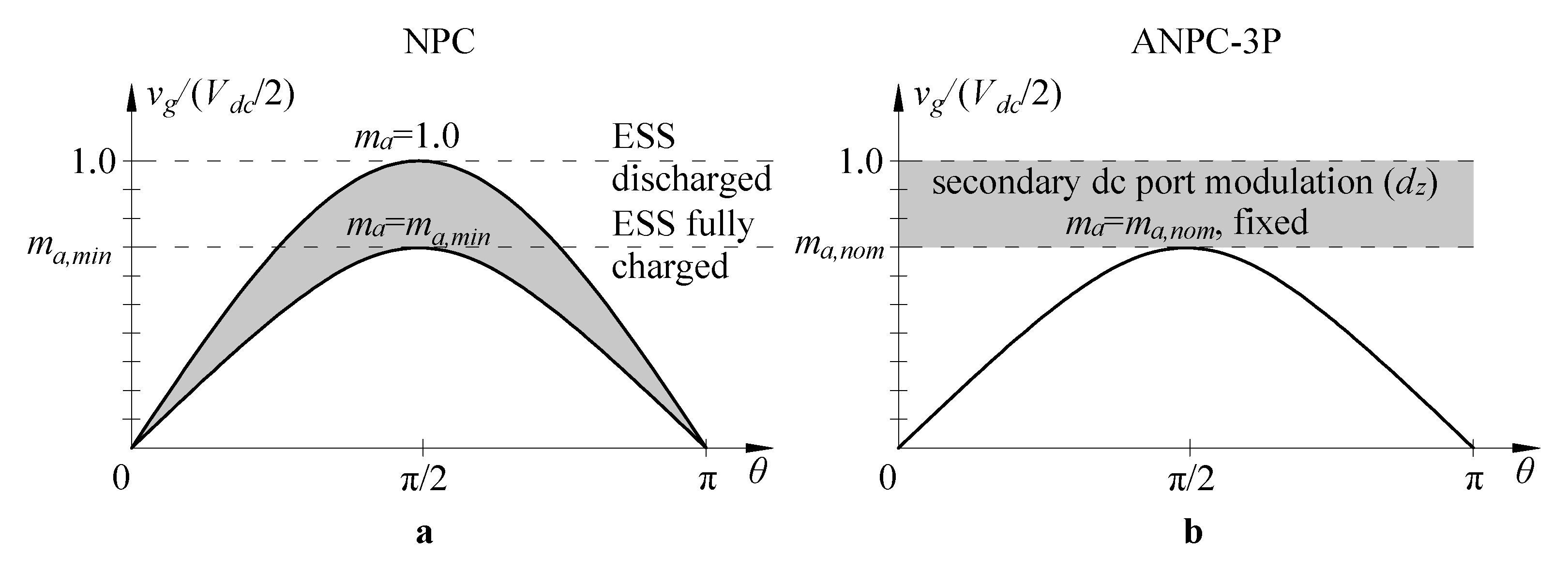
Initially, the voltage range defined in (
2) may seem a disadvantage since it is necessary to accommodate for the ESS voltage variation due its SOC. To better understand the impact of the ESS voltage variation, a comparison of the ANPC-3P topology with a configuration that uses the AC bus connection, shown in
Figure 2b, is presented. The compared configuration consists of a dedicated NPC inverter for connecting the ESS to the grid, and the ESS is connected to the DC bus of this inverter. Hypothetically, when the ESS is completely discharged the voltage
is equal to the grid peak voltage, that is, the amplitude modulation index (
) is unitary. However, when the ESS is fully charged, the voltage
increases and
presents a minimum value
. This can be better understood by looking at
Figure 5a. This range of
is required due to the voltage variation caused by the ESS SOC. Furthermore, considering the ANPC-3P inverter case, the DC bus operates with constant and maximum voltage
regardless of the ESS SOC. According to (
2), the inverter cannot operate with
close to one. The DC bus voltage must be increased to allow ESS SOC variation. This causes the inverter to operate with
below unity. According to
Figure 5b, values between
and 1.0 can be chosen to adjust the duty ratio
, as defined in (
1), to react to the variations of the ESS voltage. As a result, the DC bus voltage of the inverters in this comparison is approximately the same [
20]. To simplify the analysis, voltage drops in the filtering elements were not considered in this comparison.
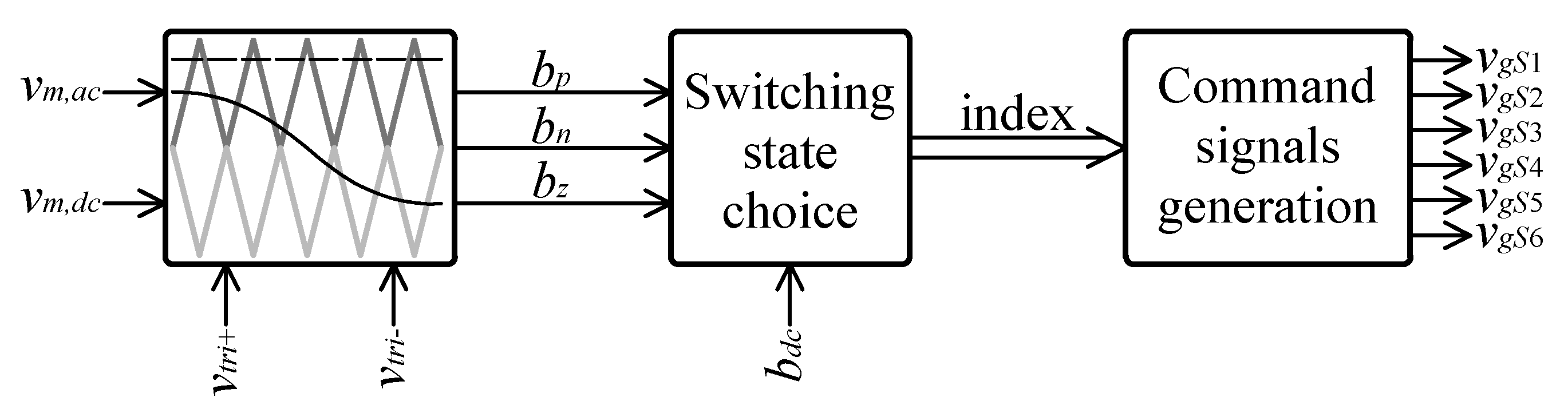
Modulation
The modulation scheme presented in this paper is based on the modulation proposed in Reference [
20]. Three blocks are used to generate the gate signals for the six switches (
), as shown in
Figure 6. The first block receives two carrier signals (
and
) in phase opposition disposition (POD) and signals
and
, which are the modulating signals of the AC port and secondary DC port, respectively. This block is responsible for comparing the modulating signals with the carriers and for generating the signals
,
and
, which are sent to the second block and contain information about the voltage levels that must be generated on both power ports. When
is high, level
must be generated in
(
is imposed in
). Signal
high indicates that
must be generated in
(
is imposed in
). Lastly,
high requests a zero level in
and
simultaneously. When all the three signals are low, level zero is applied in
and level
in
. The second block selects the appropriate switching state considering the signals computed by the first block and the available redundant switching states. The third block generates the gate signals for the six switches, including the appropriate dead times.
The ANPC-3P inverter has some redundant states and it is necessary to define how they are used. For example, states 0U3, 0U4, 0UL, 0L3, and 0L4 perform the same function considering the levels applied to the power ports. However, each state affects semiconductor devices differently. With the exception of 0UL, the other states have a single internal semiconductor device (
,
,
and
) turned off and may not allow parallelism of the upper (
–
), lower (
–
), left (
–
) and right (
–
) current paths. On the other hand, state 0UL allows the currents to flow through the four current paths. According to Reference [
24], the use of 0UL results in a simple modulation system and a small increase in the efficiency of the inverter. Thus, in this paper, only the 0UL state is used to generate the zero level simultaneously on the DC and AC ports.
States 0U1 and 0L1 play a special role in helping to balance the neutral-point voltage. Theses switching states are redundant and depending on which switching state is employed, a different effect is produced on the neutral-point potential. Therefore, by properly selecting these states, the neutral-point potential can be conveniently increased or decreased. A controller is responsible for selecting these states and this is covered in the next section.
3. Control System
The control system of the grid-tied single-phase ANPC-3P inverter is responsible for controlling the grid current (
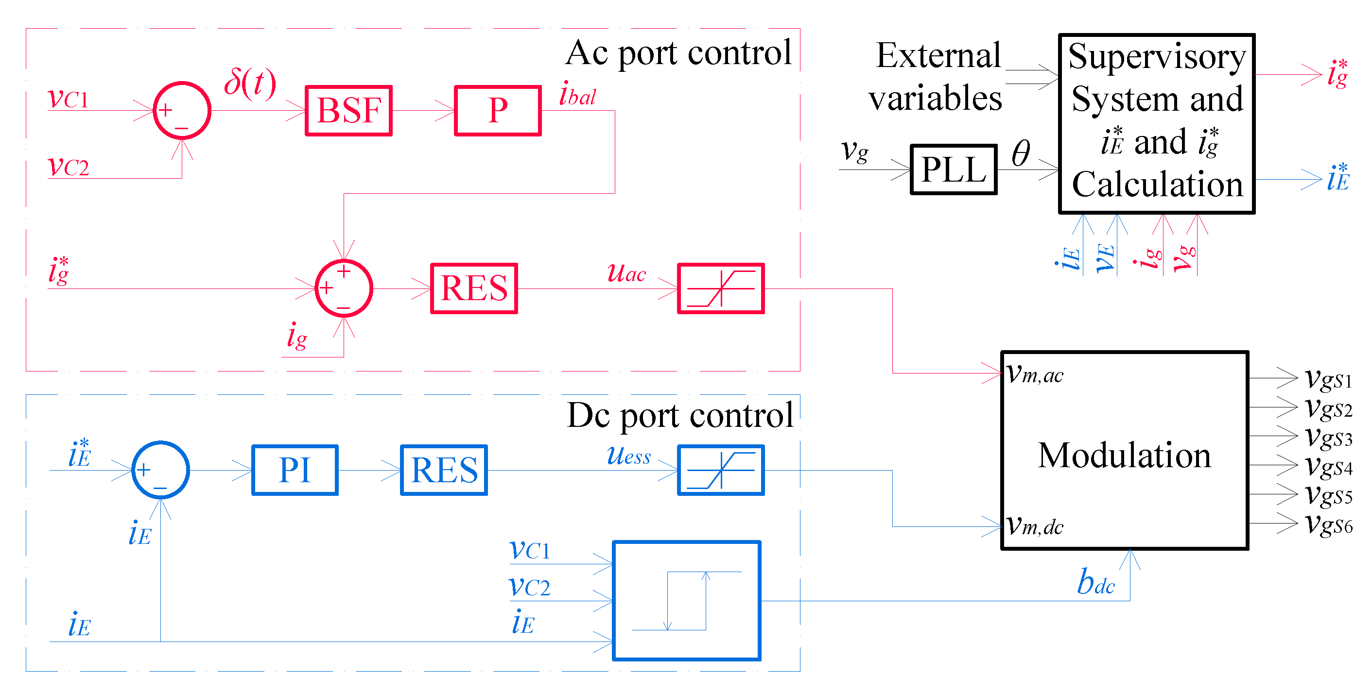
) and the ESS current and to keep the DC bus voltages balanced. The control system is composed of two subsystems—one for the AC port and the other for the ESS.
Figure 7 shows a block diagram of the proposed control system. The AC port control strategy is shown at the top (red color), and it is composed of a resonant controller (RES), aiming the grid current control, and a proportional controller, responsible for assisting in balancing the DC bus. There is also a band-stop filter (BSF) used to reject the grid frequency component from
. At the bottom (blue color), the complete ESS current control system consists of a PI (proportional-integral) controller, responsible for regulating the DC value of the ESS current, and a resonant action responsible for compensating the low-frequency ripple of the dc bus capacitors. There is also a hysteresis controller responsible for assisting in balancing the DC bus voltages by using the current
.
The supervisory system shown in
Figure 7 is responsible for monitoring the various variables involved in the operation of the grid-connected inverter and, by acting on the controller references, it defines the desired power at each port of the inverter. This supervisory system makes pre-programmed decisions to achieve certain objectives, which could be any of those ancillary services shown in
Figure 1. However, in this paper, the supervisory block is only responsible for calculating the grid voltage angle (
) and for adjusting the references of the controllers to perform some pre-programmed experiments. Details of the supervisory system are not presented in this paper.
Firstly, the AC power port control and the neutral point balancing system are presented. Afterward, the proposed controllers for the ESS current are described.
Table 2 presents the main design parameters.
3.1. Ac Port Control System
A resonant controller is used to control the current injected into the grid. Considering the grid voltage source as an infinite bus, the model of the AC port of the inverter connected to the grid can be given by:
where
is the series resistance of the filtering inductor.
The resonant controller transfer function is given by:
The pair of conjugated complex poles is allocated in the frequency () with a damping ratio of 0.001 (). The zero pair is allocated a decade below the crossover frequency with a damping ratio of . Finally, the gain is adjusted to result in a 1 kHz gain crossover frequency (approximately one decade below the switching frequency).
3.2. Neutral Point Balancing
When the ESS current is non-zero, it can help with the neutral point balancing. This can be achieved by the proper selection of states 0U1 and 0L1. These states are redundant in terms of the output voltages since they generate zero level in
and
in
. However, each state has a different impact on the DC bus capacitors, which is opposite to each other.
Table 3 presents the logic to select 0U1 and 0L1 considering the
and
voltages and
polarity. For example, if
and
, state 0U1 is selected. This state causes current
to flow into
through its positive pole. Consequently,
is charged and the DC bus voltages tend to balance. On the other hand, if
and
, state 0L1 should be used. This state causes current
to flow through
exiting from its positive pole. In this way,
is discharged aiming the equalization of the DC bus voltages. A simple way to use these states to help balancing the neutral point is to add a controller based on
Table 3. However, when
is zero its ripple causes a random selection of 0U1 and 0L1. To avoid this problem, a hysteresis band equal to the peak-to-peak battery current ripple is added to the feedback signal
.
As can be seen from
Figure 4, states 0U1 and 0L1 can be imposed during two intervals of the switching cycle:
and
. In this study, sampling is performed once in each complete switching cycle. Therefore, only one switching state is used during both time intervals.
When
or the ESS is disconnected from the inverter, it may be desirable to keep the inverter in operation and thus a mechanism to balance the DC bus voltages is required. For three-phase inverters, redundant switching states are available to synthesize a determined line voltage and, since they cause opposite impact on the DC bus voltages, these states are usually used to balance the neutral point [
25,
26,
27,
28]. Single-phase NPC/ANPC full-bridge inverters also have these redundant switching states. However, single-phase NPC/ANPC half-bridge inverters have no such redundant states and another approach should be considered. Depending on the application, a front-end converter, which is often used for other purposes, can also be used to balance the neutral point. Some works propose the use of a dedicated balancing circuit [
29,
30]. Another technique is the insertion of a DC signal into the modulating signal of the AC port [
31] or into the current reference [
32].
During the positive semicycle of the synthesized AC output voltage of the inverter, the power is delivered by capacitor
. During the negative semicycle, capacitor
performs this function. In normal operation, the power delivered in the positive semicycle must be equal to that of the negative semicycle so that the current
are equal in both semicycles and the DC current is zero [
32,
33]. In practice, due to small discrepancies in the inverter or instrumentation errors, it is expected that a DC component will appear in the grid current and that will cause the DC bus capacitors voltages to become unbalanced. This unwanted DC component can be compensated by a control system. In this sense, the inclusion of a control loop capable of compensating for differences in the average voltages of the DC bus capacitors is proposed. This control action (
) is summed with the grid current reference (
).
The transfer function between the voltage in the capacitor
and current
is ideally given by:
where
and
is the peak voltage at PCC (Point of Common Coupling), which is the point where the inverter is connected to the utility grid.
A simple proportional compensator is proposed to generate the balancing current . The gain was adjusted to result in a crossover frequency of 6 Hz and phase margin of 90°. This corresponds to a settling time of approximately 100 ms.
The error signal
can be extracted from the DC bus capacitors voltages using:
This signal presents ripple mainly in the grid frequency. To improve the compensator performance, one can add a band-stop filter (BSF) to the error signal. As a result, the compensator only acts at the DC value of . Without the BSF filter, the compensator could interfere with the grid reference current and lead to steady state errors. In this paper, a second order BSF filter was designed with a center frequency of 60 Hz and a 20 Hz stop band.
3.3. ESS Control System
The current control of the ESS is composed of the cascade association of PI and resonant controllers. The PI compensator is responsible for ensuring zero steady-state error for step inputs and for adjusting the transient response. A resonant control action is responsible for compensating the low frequency current ripple.
Initially, to design the PI controller, the control-to-output transfer function of the secondary DC port is needed, which is given by:
where the resistance
is the sum of all series resistances, such as the inductor resistance (
) and the ESS internal resistance (
), and so forth. The PI controller transfer function is:
where
is the integral time constant and
is the proportional gain.
A response in the order of a few milliseconds and with minimum overshoot for the current
is desirable. The zero of the controller is placed to cancel the plant pole, that is,
. Thus, the closed-loop system can be approximated by a first order system, and the proportional gain can be defined as:
where
is the time constant of the resulting closed-loop first order system. Considering the parameters shown in
Table 2 and
ms, the resulting controller gains are:
and
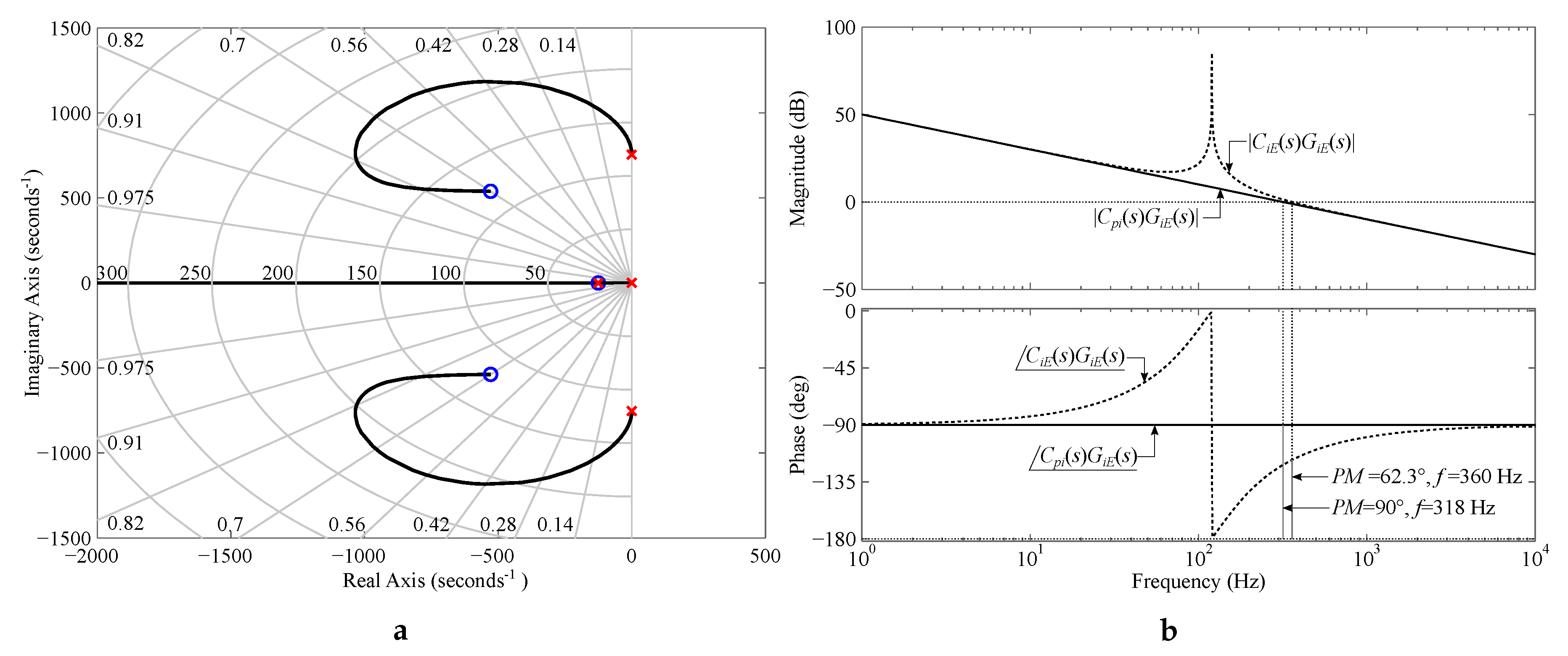
s. These gains correspond to a crossover frequency equal to 318 Hz and phase margin of 90 degrees.
The design of the resonant compensator was carried out similarly to that presented for the AC current control. Signal
has a dominant frequency at 60 Hz. In this way,
also changes its logic level at the same frequency. However, the ESS current is also affected when the
polarity changes. Therefore, the low-frequency ripple in the ESS current is twice the grid frequency. Considering (
4), the pair of conjugated complex poles is allocated in the frequency
(
) with a damping ratio of 0.001 (
). The zero pair is allocated at the same frequency
but with a damping ratio of
and the gain
is set to 1 to keep the PI response unchanged at lower frequencies. The complete transfer function of
controller is given by:
Figure 8 presents the root locus and the Bode diagram for the ESS current control loop. As can be seen, the inclusion of the resonant controller causes a little change in the crossover frequency and the phase margin becomes 62.3 degrees.
4. Experimental Results and Discussions
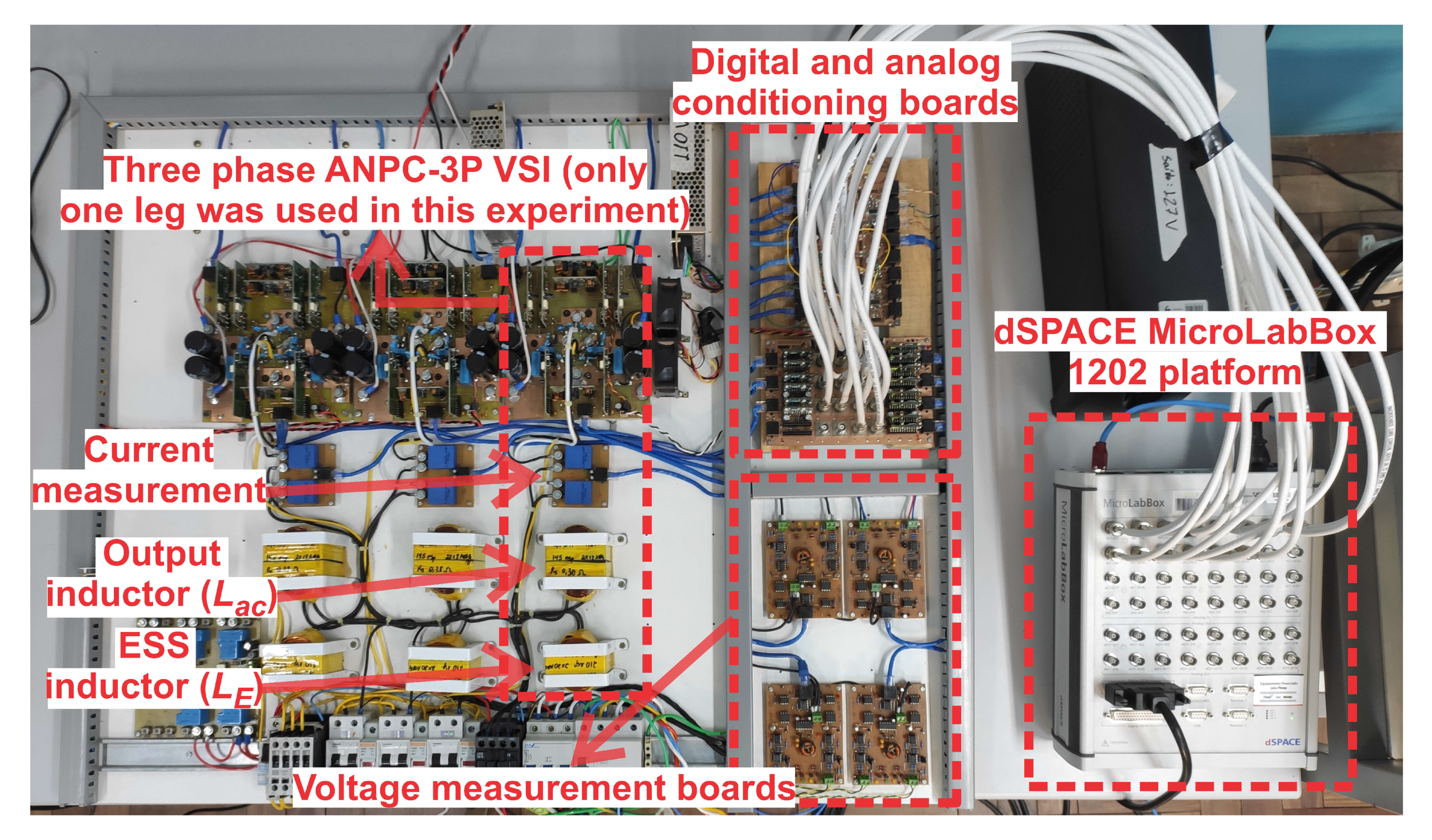
The ANPC-3P inverter was designed according to the specifications listed in
Table 2. The experimental setup is shown in
Figure 9. The modulation and control systems described in this study were implemented in the dSPACE MicroLabBox 1202 platform. The inverter is composed of six IGBTs IRGP50B60PD1. The current transducers are LEM LA-25NP and the voltage measurement boards were designed based on HCNR201 optocouplers. The experiments were conducted with the DC bus connected to a DC power supply. The ESS consists of 23 valve-regulated lead acid (VRLA) batteries of 12 V and 7 Ah. The battery charging current is limited to −2 A.
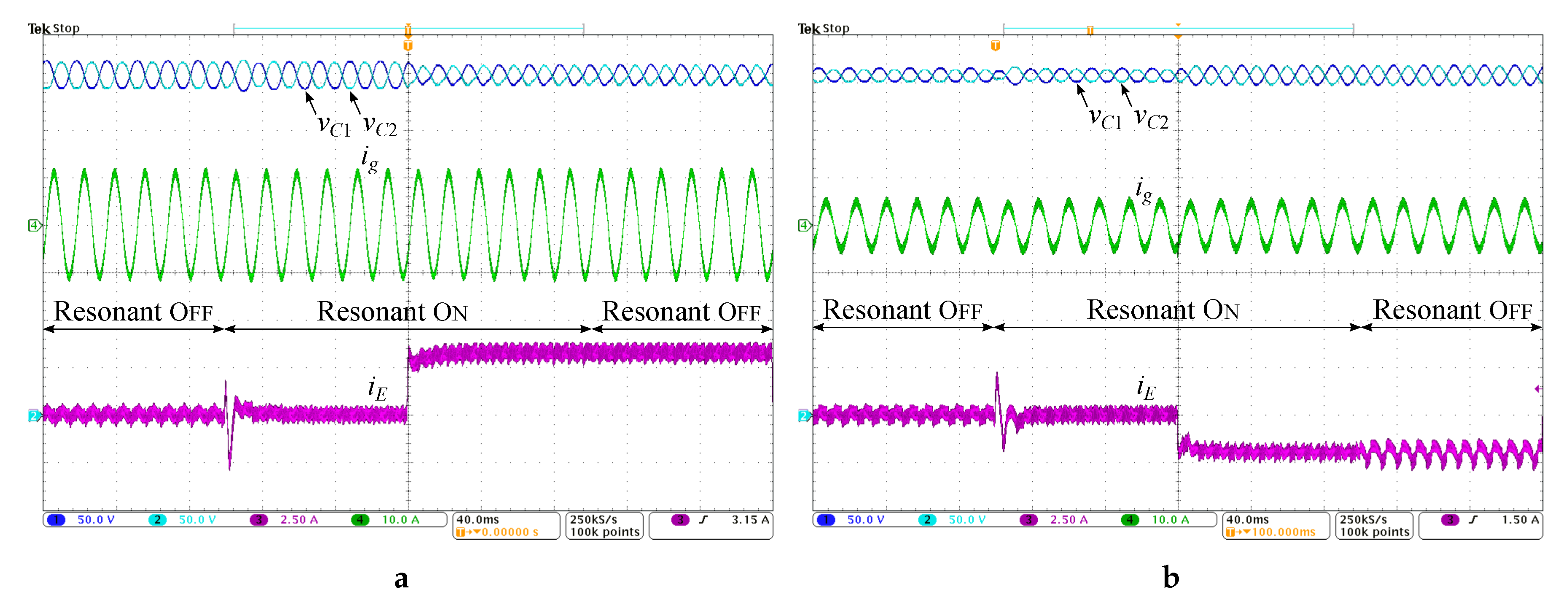
Figure 10 shows experimental results when the resonant control action is turned on and off in the
control loop. The experiments begin with the resonant controller off. It can be seen that there is 120 Hz ripple in the current
. Considering the time reference of the oscilloscope trigger, in
ms the resonant control action is turned on. After the transient produced by the inclusion of the controller, the current
presents mostly high frequency ripple. Considering the
Figure 10a, in
ms a discharging step of 3.33 A is performed on the ESS. After this moment, the ESS provides approximately the full power injected into the grid. Additionally, the step in the ESS current
does not cause significant disturbance to the current
and the voltages across the DC bus capacitors remain balanced. It is also noted that the switch-off of the resonant controller during discharge mode in
ms has little visible effect. In
Figure 10b, in
ms, a charging step of −2 A was performed on the ESS. The current injected into the grid was reduced to keep the nominal power (1 kW) processed by the inverter. In charging mode, at
ms the resonant controller is turned off and a significant 120 Hz ripple appears in
. In ESS recharge mode, resonant compensator reduces the current ripple of
by approximately 0.5 A peak-to-peak.
Figure 11 shows experimental results when current steps are applied on both power ports to verify dynamic performance. In these experiments, the resonant controller of
is kept on. In
Figure 11a the power injected into the grid is always positive. At the time reference of the oscilloscope trigger, in
ms the power injected into the grid is increased. After, in
ms, the ESS starts to discharge with partial power compensating the power reduction of the main dc source. In
ms grid power is reduced and it is fully supplied by the ESS (
power is near zero). Afterward, in
ms, ESS goes to recharge mode and the power injected into the grid is kept positive and constant. It can be noted that the proposed control system can maintain controlled currents and quickly reject disturbances.
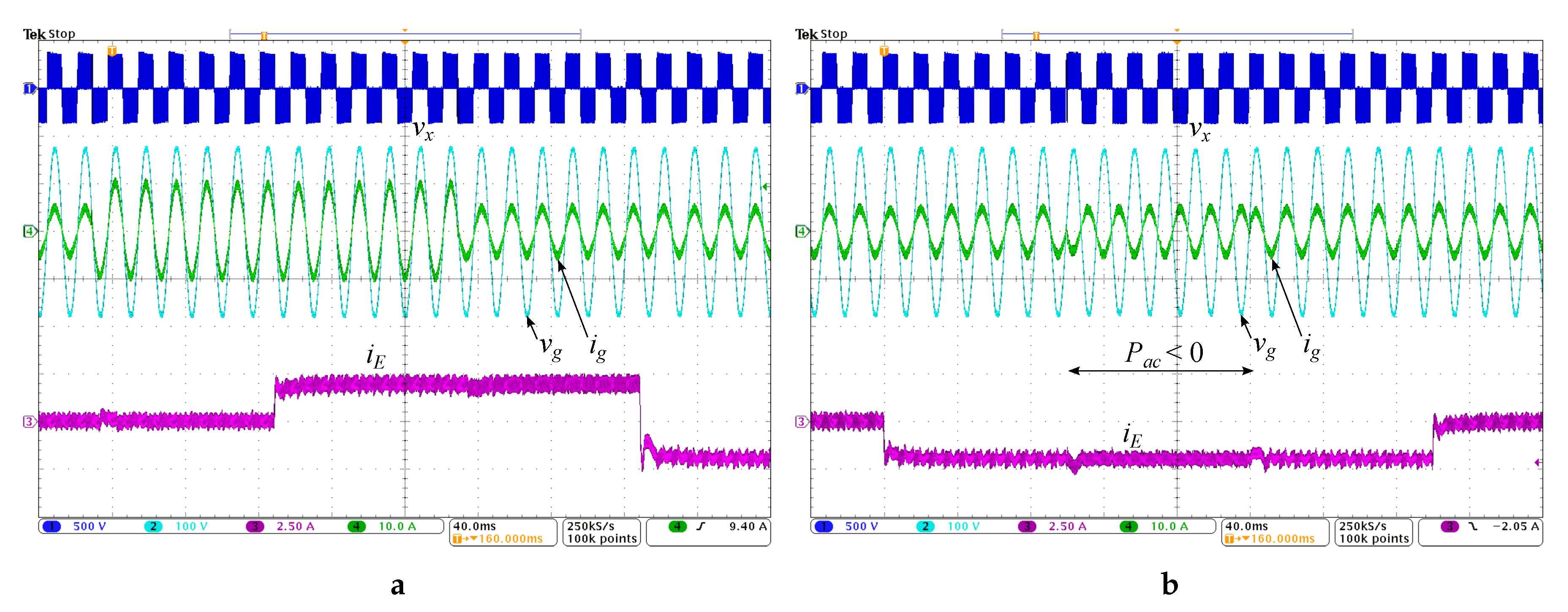
In
Figure 11b an experiment is shown in which the grid is charging the ESS for a certain period. At the time reference of the oscilloscope trigger, in
ms the ESS is switched to charging mode. The power injected into the grid is positive and constant, that is, the DC bus provides power for both the grid and the ESS. Approximately at
ms, power is drawn from the grid to supply the ESS power demand. In photovoltaic applications this condition can occur at night and/or when energy is cheaper. Then, in
ms power is injected into the grid again. Finally, in
ms the ESS returns to its initial state (floating).
As shown in the experimental results, current steps performed in one power port caused a slight disturbance in the current of the other port. The modulation and the control systems of each port are independent. These disturbances occur because both ports are connected to the same DC bus. Thus, a step on one port causes disturbances in the DC bus voltages that are reflected to the other port.
During the experiments, measurements focusing on the quality of the current injected into the grid were taken. A Yokogawa WT1800 precision power meter was used to perform the measurements. When the rated current of the inverter was applied, the DC component injected into the grid was below 10 mA. The THDi was approximately 5% considering the rated AC current. The measuring equipment was configured to calculate up to the 500th harmonic (30 kHz).
5. Conclusions
The ANPC-3P topology proves to be an interesting option for grid-tied distributed generation applications, mainly when the inclusion of energy storage systems is required. A detailed analysis of the control system for this topology is presented in this paper. Special attention should be given to the control strategy of the ESS current. In addition to the ripple of the DC bus voltages caused by the pulsed behavior of AC power, there is the possibility of applying the voltage from either pole of the DC bus in . Depending on how the DC bus pole is selected, current may present random disturbances that are more difficult to compensate. In this study, the inclusion of the hysteresis function when calculating proved to be crucial for the correct functioning of the resonant compensator.
The experimental results demonstrate that the designed control system is capable of injecting a sinusoidal current into the grid, balance the neutral point voltage and regulate the ESS current with reduced low-frequency ripple. Both power ports of the inverter have been subjected to different operating modes, typical of grid-tied renewable generation, including the reverse power mode, in which the ESS is charged from the utility grid.


