Article

Step-Up Series Resonant DC–DC Converter with Bidirectional-Switch-Based Boost Rectifier for Wide Input Voltage Range Photovoltaic Applications

Department of Electrical Power Engineering and Mechatronics, Power Electronics Group, Tallinn University of Technology, 19086 Tallinn, Estonia
*
Authors to whom correspondence should be addressed.
Energies 2020, 13(14), 3747; https://doi.org/10.3390/en13143747
Submission received: 25 June 2020 / Revised: 13 July 2020 / Accepted: 17 July 2020 / Published: 21 July 2020

Abstract

:
This paper proposes a high gain DC–DC converter based on the series resonant converter (SRC) for photovoltaic (PV) applications. This study considers low power applications, where the resonant inductance is usually relatively small to reduce the cost of the converter realization, which results in low-quality factor values. On the other hand, these SRCs can be controlled at a fixed switching frequency. The proposed topology utilizes a bidirectional switch (AC switch) to regulate the input voltage in a wide range. This study shows that the existing topology with a bidirectional switch has a limited input voltage regulation range. To avoid this issue, the resonant tank is rearranged in the proposed converter to the resonance capacitor before the bidirectional switch. By this rearrangement, the dependence of the DC voltage gain on the duty cycle is changed, so the proposed converter requires a smaller duty cycle than that of the existing counterpart at the same gain. Theoretical analysis shows that the input voltage regulation range is extended to the region of high DC voltage gain values at the maximum input current. Contrary to the existing counterpart, the proposed converter can be realized with a wide range of the resonant inductance values without compromising the input voltage regulation range. Nevertheless, the proposed converter maintains advantages of the SRC, such as zero voltage switching (ZVS) turn-on of the primary-side semiconductor switches. In addition, the output-side diodes are turned off at zero current. The proposed converter is analyzed and compared with the existing counterpart theoretically and experimentally. A 300 W experimental prototype is used to validate the theoretical analysis of the proposed converter. The peak efficiency of the converter is 96.5%.

1. Introduction

Nowadays, with climate change around the world being evident, electrification is considered as a viable solution for the energy transition [1]. Therefore, power electronic converters face numerous new applications [2]. Among different emerging applications, there is a demand for high-performance DC–DC converters suitable for the integration of low-voltage energy sources and battery energy storage in DC microgrids [3]. In some cases, like photovoltaic (PV) module-level power electronic applications, both high-voltage step-up and the wide input voltage range regulation capability are required to interface individual PV modules that can supply their maximum power at very different voltages due to shading effects [4]. Therefore, the associated DC–DC interface converter has to regulate the input voltage in a wide range while providing high efficiency to draw the maximum available power from a PV module.
Usually, high-voltage step-up applications require galvanic isolation as a high-frequency transformer to step up voltage efficiently. Several DC–DC converters have been proposed to solve the voltage variation [5,6,7]. These topologies vary in their structure, complexity, and other aspects. The isolated buck-boost converters were justified as a suitable solution for high step-up wide-range applications. Usually, they have active switches at both sides of the converter to implement voltage buck and boost functionalities on different converter sides. Among these topologies, the series resonant converters (SRCs) have demonstrated high performance in target PV applications. They provide soft-switching of semiconductor components and good utilization of the isolation transformer [8,9]. The SRC topology is similar to the LLC converter topology that is investigated in many industrial applications [10,11]. However, the ratio between the magnetizing and the resonant inductances is several times higher in the SRC compared to the LLC converter. In general, the resonant converter applies the frequency modulation to control the DC voltage gain. However, this study targets low-power compact SRCs that use a small (low-cost) resonant inductor in the resonant tank. Even though such implementation results in low values of the quality factor, their DC voltage gain can be controlled using the pulse width modulation (PWM), which simplifies the converter design.
In the galvanically isolated buck-boost SRCs, the input voltage buck functionality is usually implemented by PWM [12] or phase-shifted modulation (PSM) [13] of the front-end inverter. These modulation methods have been already verified in numerous studies that date back as far as 1988 [12]. From the recent reports, it could be concluded that the highest efficiency is achieved for the input voltage buck operation by using PSM and hybrid PSM methods [14]. Currently, much attention is given to the input voltage boost implementation in the SRC [8]. The implementation of a boost rectifier usually achieves this [15]. As this study targets high-voltage step-up applications, the boost rectifiers are based on the voltage-doubler rectifier (VDR) to minimize the transformer turns ratio. Typical boost VDR is based on replacing diodes with the metal oxide semiconductor field-effect transistors (MOSFETs) and their control with short pulses [16] or double-pulse modulation [17]. Power losses in the boost VDR could be reduced if only one diode is replaced with a MOSFET, which, however, results in higher peak current of the resonant inductor and thus can compromise its size [9]. On the other hand, the implementation of a four-quadrant bidirectional switch in parallel to the transformer secondary winding allows for a significant reduction of the switch voltage stress and thus switching losses. At the same time, it keeps the positive and negative magnitudes of the resonant current balanced. Due to these advantages, topology in [18] is considered in this study. Comprehensive analysis shows that this topology cannot operate in a wide range of voltages and power. Therefore, a new converter is proposed to extend the input voltage regulation range by rearranging positions of the resonant tank elements. The proposed converter topology is based on the topology in [18], where the position of the resonance capacitor is moved to be placed between the bidirectional switch and the transformer secondary winding. The proposed converter is feasible in a wide range of the resonant inductance values without affecting the input voltage regulation range, which is not feasible for the baseline topology from [18]. This paper proposes a new SRC topology with a modified boost VDR and verifies it in the voltage range suitable for the module-level PV applications. The main hypothesis is that it is possible to extend regulation voltage and power range of the baseline topology by rearranging the resonant capacitor position. There are three main contributions: identification and experimental verification of the limits of the input voltage and power regulation range in the converter [18], synthesis of the converter with improved input voltage and power regulation range, and derivation of its steady-state mathematical model that is verified experimentally.
The rest of the paper starts with Section 2 that describes the proposed topology and provides its comprehensive analysis. Section 3 presents a comparison between the proposed and the baseline SRC topology. The results of experimental verification are discussed in Section 4. Finally, Section 5 draws the conclusion.

2. Topology Description and Modulation

2.1. Topology Description

The configurations of the proposed and conventional topologies are shown in Figure 1a,b, respectively. The proposed topology employs the voltage-doubler rectifier in the output side. The resonance capacitor (Cr) is placed before the bidirectional switch in the proposed topology. At the same time, it is integrated as part of the voltage-doubler rectifier in Figure 1b. In the proposed SRC topology, the capacitors C1 and C2 have much larger capacitance than Cr to keep the resonance frequency ( f r ) constant according to (1). The value of resonance inductance L r equals either the value of the isolation transformer leakage inductance ( L l k ) or the sum of the transformer leakage inductance and the external inductance ( L e x t ) if the leakage inductance is low. The cost and size of the converter can be reduced by utilizing only the transformer leakage. The average voltage of the resonant capacitor (VCr) equals zero due to the symmetry of the VDR during the switching period as will be explained later. Contrary to the topology [18], the average voltage across the resonant capacitors (Cr/2) equals half of the output voltage (i.e., VOUT/2). The bidirectional switch comprises the two MOSFETs Q1 and Q2. The conventional voltage-source full-bridge inverter is employed at the input side. The transistors of the input-side bridge are driven with complementary pulses of nearly 0.5 duty cycle, considering a small dead time between the control signals in the same leg. The input-side full-bridge inverter feeds the isolating transformer TX with a balanced rectangular voltage that features positive and negative magnitudes equal to the input voltage. The magnetizing inductance of the transformer ( L m ) provides auxiliary circulating current that assists the soft switching of the primary-side transistors. The magnetizing current can recharge their parasitic output capacitance during the short dead times. The isolating transformer TX steps up the voltage fed by the input bridge inverter by the turns ratio n.
f r = 1 2 π L r C r
where, Lr is the resonant inductance.

2.2. PWM Schemes for the Boost VDR

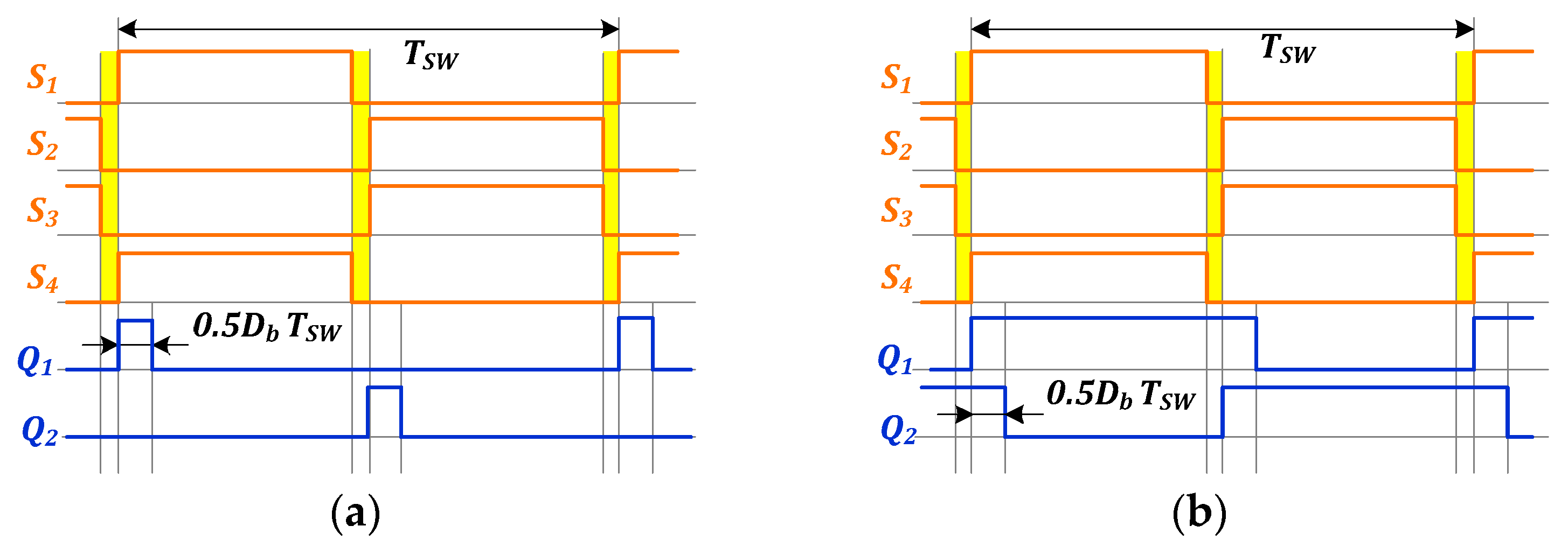
The switches Q1 and Q2 form the bidirectional switch. They are used to short-circuit the transformer output winding; so, the resonant inductor can increase its energy serving as a boost inductor of the AC boost converter. The two switches are connected in the back-to-back configuration. The bidirectional switch allows its current to flow in both directions, while it can block both voltage polarities. Two PWM schemes could be employed to generate the gating signal for the switches Q1 and Q2, as shown in Figure 2. First, only one of the switches is turned on at each half-cycle and forms a path for the current through the body diode of the other switch, as shown in Figure 2a. For example, during the positive voltage half-wave across the transformer secondary winding, the transistor Q1 is turned on, which results in the conduction of the body diode of the transistor Q2. In the other PWM scheme from Figure 2b, the switches are controlled with overlapped signals of equal duty cycle, which are shifted regarding the control signals of the input-side switches. Therefore, the body diodes are not used at all, and synchronous rectification is implemented to reduce the conduction losses. In both cases, the switching frequency of the switches Q1 and Q2 is the same as that of the primary-side switches. The voltage boosting mode occurs during two equal time intervals with the cumulative duty cycle Db, which are separated in time by half of the switching period TSW.
The peak-to-peak ripple of the capacitor voltage is affected by the output power level (POUT), as given in (2). It is worth mentioning that the proposed topology can operate with the PWM technique from Figure 2b in a limited range of power and voltage. Abnormal operation occurs when the maximum capacitor voltage is larger than the voltage of the transformer secondary winding (i.e., ΔVCr/2 > n⋅VIN). As shown in Figure 3, when a positive voltage feeds the secondary winding of the transformer, the current begins to flow in the reverse direction after discharging the stored energy. This reverse current increases the conduction losses of the converter, which results in the deterioration of the system efficiency and reduction of the DC voltage gain.
Δ V C r = P O U T T S W 2 n V I N C r ,
where TSW is the switching period, n is the transformer turns ratio, and VIN is the input voltage.

3. Steady-State Analysis and Comparison

3.1. Description of the Operating Principle

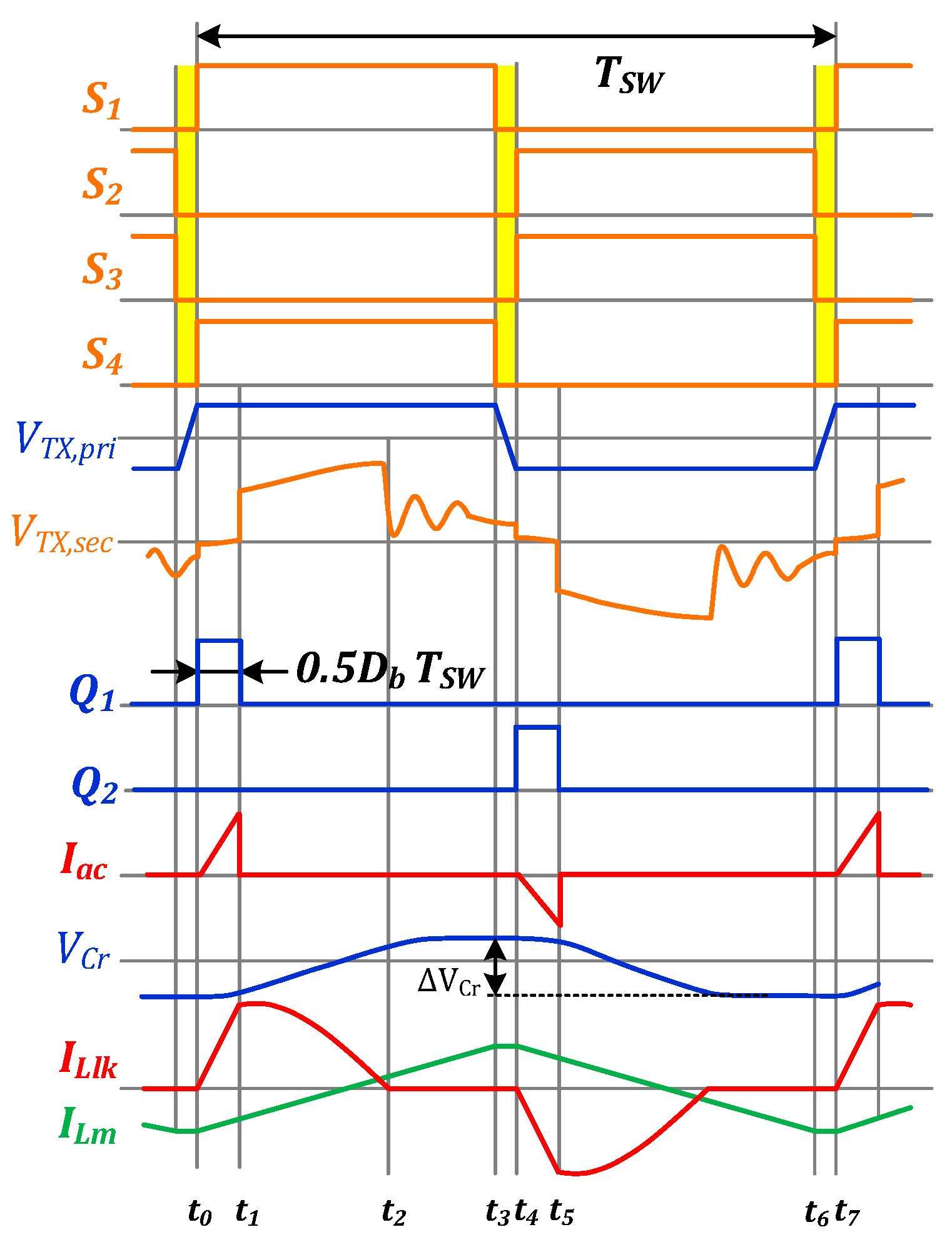
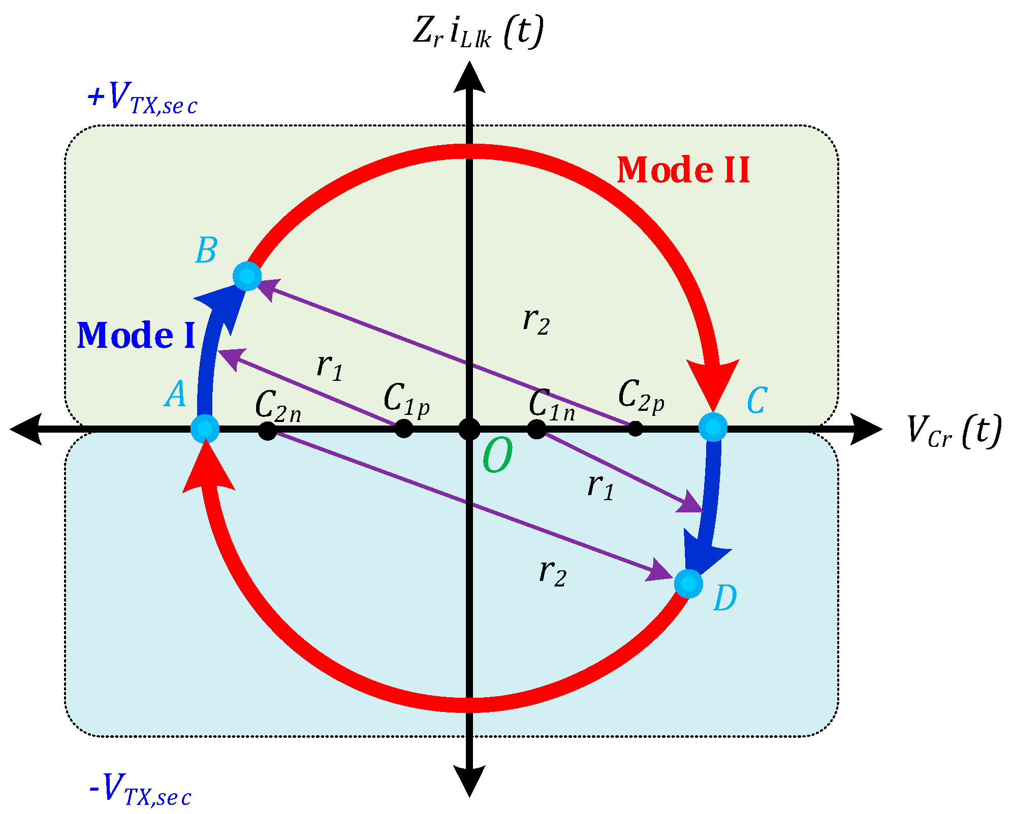
The main voltage and current waveforms of the proposed topology and the state-plane trajectory of the state variables are given in Figure 4 and Figure 5. The resonant current (iLlk(t)) is multiplied by the resonant impedance Zr defined in (3) to have the same units of the axes. The steady-state analysis was performed based on the following assumptions:
  • The output voltage (VOUT) is ripple-free due to the high value of the output capacitance (CO).
  • The output capacitances (C1, C2, CO) are much larger than the resonant capacitance (Cr).
  • The PWM scheme in Figure 2a is applied to the switches Q1, Q2.
  • The system is lossless.
    Z r = L l k C r .

3.2. Modes of Operation

Mode I [t0 < t ≤ t1]: This time interval corresponds to the first half of the voltage boosting mode with the duty cycle of Db/2. A positive voltage is applied to the transformer primary winding by turning on the switches S1 and S4 and the secondary winding voltage equals nVIN. For better understanding, the equivalent circuit of this interval is given in Figure 6a. The resonance capacitor voltage has a minimum value of - Δ V C r / 2 at the time instant t0. Also, the initial resonance current is nearly zero prior to turning on the switch Q1 that will be turned on at nearly zero current switching (ZCS) conditions. The voltage of the resonant capacitor assists the secondary winding voltage to accelerate the current charging of the resonant inductor, similar to the conventional boost converter. On the state-plane, the voltage of the resonant capacitor moves from point A to point B during this time interval with roughly sinusoidal shape, as shown in Figure 5. The state variable equations for the resonance current and voltage can be expressed in time domain as in Equations (4) and (5), respectively.
i L l k ( t ) = r 1 Z r s i n ( π ω r ( t t 0 ) ) ,
v C r ( t ) = n V I N + r 1 c o s ( π ω r ( t t 0 ) ) ,
r 1 = n V I N + Δ V C r 2 ,
where r1 refers to the radius of the trajectory arc segment with center at (nVIN; 0), ω r = 2 π f r is the angular resonance frequency in rad/s.
Mode II [t1 < t ≤ t2]: The switch Q1 is switched off and the bidirectional switch current Iac drops to zero. The stored energy in the resonant inductor is releasing directly to the load, as shown in Figure 6b. The diode D1 begins to conduct as it has a forward-biased state. The current of the resonant inductance is still flowing in the same direction with reversed voltage polarity, that is, it equals (VOUT/2 − nVIN) at the instant t1. During this interval, the resonant inductor resonates with the resonant capacitor, and therefore, the resonance capacitor voltage moves from point B to point C along the trajectory curve. The length of this path is represented by the angle β (in rad). The capacitor voltage reaches its maximum value at Δ V C r /2, and the resonant current reaches zero at the instant t2. Equations (7)–(9) describe the converter operation in this mode before the resonant current drops to zero.
i L l k ( t ) = r 2 Z r s i n ( β ω r ( t t 1 ) ) ,
v C r ( t ) = n V I N V O U T 2 + r 2 c o s ( β ω r ( t t 1 ) ) ,
r 2 = n V I N + V O U T 2 + Δ V C r 2 ,
where r2 refers to the radius of the arc trajectory segment with center at ((nVINVOUT/2); 0).
Mode III [t2 < t ≤ t3]: The resonant current equals zero as all the stored energy is released into the load in the previous mode, and the diode D1 is turned off at ZCS. Consequently, the converter enters the discontinuous conduction mode (DCM) and no energy is transferred to the load during this mode. The capacitor voltage remains constant at its maximum value at Δ V C r /2 until the end of this period at TSW/2.
Mode IV [t3 < t ≤ t4]: This refers to the dead-time interval and the primary switches (S1, S4) are turned off at t3. The magnetizing current denotes the circulating current referred to the primary winding to charge/discharge the parasitic output capacitance of switches (S1, S4) and (S2, S3), respectively. Therefore, the voltage across the switches (S2, S3) equals zero before the time instant t4. The values of the dead time and the magnetizing inductance are interdependent and must ensure full discharging of the switch parasitic capacitances. This allows the primary switches to be turned on at zero voltage switching (ZVS) conditions.
Mode V [t4 < t ≤ t0]: This represents the negative half-cycle of the switching period. The converter operates similar to that during time interval [t0; t4].

3.3. DC Voltage Gain Derivation

The segments of the state-plane trajectory of the resonant tank that correspond to the positive and negative half-cycles are symmetric. Therefore, only the trajectory segment A-B-C is considered to derive the DC voltage gain expression for the proposed converter. The general expressions for the circle radius in Modes I and II are given by Equations (10) and (11), respectively. The two circles intersect at point B, which results in (12).
r 1 2 = ( v C r n V I N ) 2 + ( Z r i L l k ) 2 ,
r 2 2 = ( v C r n V I N + V O U T 2 ) 2 + ( Z r i L l k ) 2 ,
( v C r ( t 1 ) n V I N ) 2 + ( Z r i L l k ( t 1 ) ) 2 r 1 2 = ( v C r ( t 1 ) n V I N + V O U T 2 ) 2 + ( Z r i L l k ( t 1 ) ) 2 r 2 2 .
The resonant inductor current and resonant capacitor voltage at the instant t1 can be given as:
i L l k ( t 1 ) = r 1 Z r s i n ( ω r t 1 ) ,
v C r ( t 1 ) = n V I N + r 1 c o s ( ω r t 1 )
The resonance path angle β is derived from Equations (7) and (13) as follows:
β = π s i n 1 ( r 1 r 2 s i n ( ω r t 1 ) ) .
Then, by substituting t 1 = D b T S W / 2 in Equations (13)–(15), the cumulative duty cycle of the converter can be expressed as:
D b = 2 c o s 1 ( T S W P O U T 4 C r ( 4 G n ) + n V I N V O U T n V I N V O U T + T S W P O U T 4 C r G n ) ω r T S W   ,
where G n = V O U T n V I N is the normalized DC voltage gain.
It follows from Equation (16) that the duty cycle depends not only on the level of the converter output power but also on the resonance tank parameters.
For the topology in [18], the duty cycle Db is given in Equation (17).
D b = 2 L l k 2 P O U T T S W V O U T C r ( V O U T n V I N ) Z r n V I N T S W .

3.4. Comparison of DC Voltage Gain and Input Operating Range

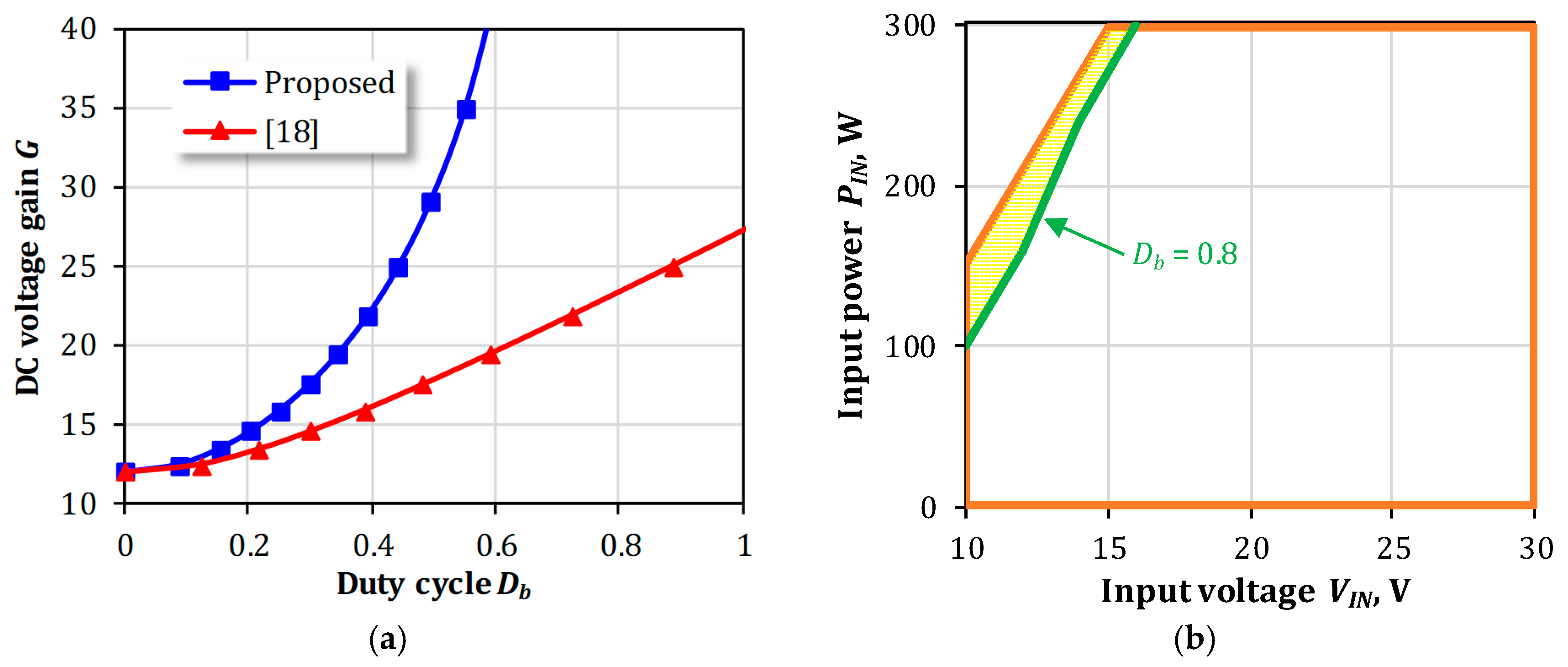
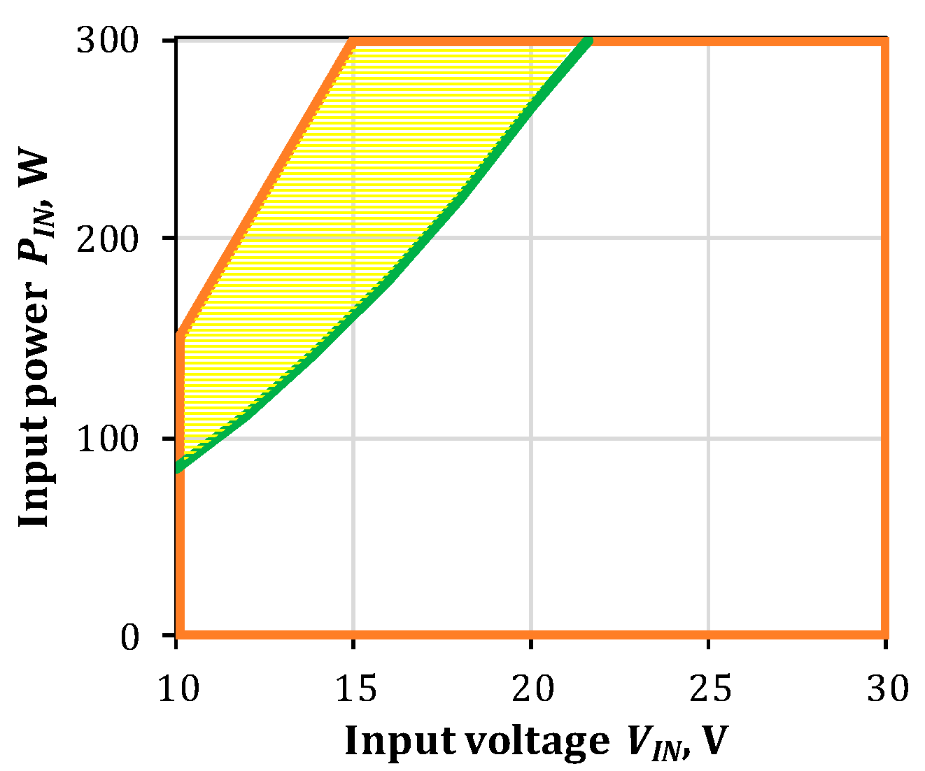
This section provides a comparison between the proposed and the baseline [18] topologies. The main feature of the proposed topology is the input voltage regulation in a wide voltage and power range. The superiority over the baseline SRC topology is achieved as the proposed converter can provide much higher DC voltage gain at the same duty cycle Db, as shown in Figure 7a. Moreover, the proposed converter is much less sensitive to the value of the resonant inductor, while the baseline SRC topology shows a strong dependence of the available voltage and power regulation range on the resonant inductance value. Based on Equation (16), the operating range limit is shown in Figure 7b where it is compared to the target operating range defined by the maximum input current IINm = 20 A, the maximum input power PINm = 300 W, and the maximum input voltage VINm = 30 V, while the minimum input voltage is limited to 10 V to limit the converter power loss. The given target operating range is typical for module-level PV applications, as the interface converter should be capable of operating under partial shading, when the global maximum power point can occur at voltage as low as 10 V. The area highlighted with yellow color shows the region where the baseline SRC topology from [18] cannot operate as the limiting line is drawn theoretically for a critical case of Db = 0.8. In practice, the duty cycle value is always below unity Db < 1, which means that experimental regulation range of the baseline topology will be even more limited than that in Figure 7b.

4. Experimental Results

4.1. Description of the Experimental Prototype

A 300 W prototype was built to demonstrate the feasibility of the proposed converter. The parameters and components used in the setup are listed in Table 1. The converter is designed for the target operating range shown in Figure 7b, which suits the PV applications and is similar to the previous studies [18,19,20]. Only generic Si MOSFETs are used in the input side to reduce the converter cost. The use of SiC devices at the output side is unavoidable due to high switching frequency.
The isolating transformer was built on an ETD39 core of 3C95 ferrite material. The transformer turns ratio n = 6 yields the output voltage of 350 V according to (18), which results in the boost mode at the input voltage below 30 V. The value of the output voltage is suitable for the integration with residential DC microgrids. The number of primary and secondary turns equals 9 and 54, respectively. This design yields the maximum flux density of the core of 60 mT in the worst case. Therefore, the core losses can be minimized. To reduce the skin effect and proximity losses in the transformer, 90 × 0.2 and 90 × 0.1 litz wires were used for the primary and secondary windings, respectively. They were interleaved to reduce the leakage inductance and insulated by the Kapton polyimide tape to minimize the capacitance between the layers. An external inductor was connected in series with the secondary winding of the transformer to increase the resonance inductance. The resonance frequency of the converter was aimed close to the switching frequency to ensure the ZVS of the primary-side MOSFETs [9]. The dead-time period between S1, S2 or S3, S4 equaled 190 ns. The PWM control signals were generated using the low-cost microcontroller STM32F334. The system efficiency was measured by a Yokogawa WT1800 precision power analyzer.
n = V O U T 2 V I N m .

4.2. Steady-State Waveforms

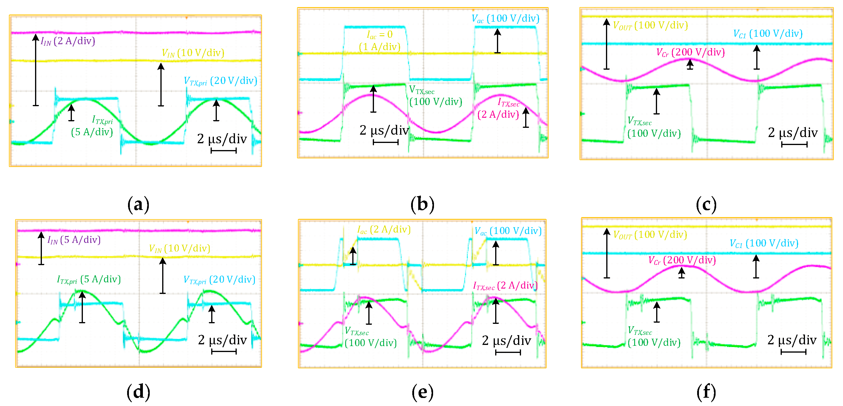
The steady-state experimental waveforms of the proposed converter at the maximum input voltage are given in Figure 8a–c. The operating power was 300 W and the bidirectional switch was turned off. The primary switches S1,2,3,4 were driven with a nearly 0.5 duty cycle, so the primary winding voltage of the transformer had the square shape in Figure 8a. The proposed converter operated in the DC transformer (DCX) mode. The peak-to-peak voltage of the transformer primary was 60 V and the input current equaled 10 A. The primary current was a periodic sine wave with a peak value of 8 A. The oscillations appeared in the primary winding voltage and current due to the parasitic capacitances of the semiconductors. In Figure 8b, the bidirectional switch had zero current and the peak-to-peak voltage of 350 V. The secondary winding voltage had the same shape of the primary winding voltage, but the magnitude was multiplied by n (i.e., 180 V). The peak value of the secondary winding current was 2.4 A. The theoretical and measured peak-to-peak of the resonance capacitor voltage was 174 and 175, respectively. These values are well-matched, which proves the theoretical analysis. The output voltage was constant at 350 V and C1 had half of the output voltage (i.e., 175 V). The voltage swing of the resonant capacitor equaled 300 V, which was slightly higher than the calculated value of 280 V.
For the converter operation in the boost mode, the steady-state voltage and current waveform are given in Figure 8d–f. The operating power was PIN = 300 W and the input voltage equaled VIN = 25 V. The cumulative duty cycle of the bidirectional switch equaled Db = 0.215. The drawn current from the supply equaled 12 A. The average voltage of the resonance capacitor was zero and the peak-to-peak ripple voltage equaled roughly 230 V. The output voltage was constant at VOUT = 350 V. Small parasitic oscillations occurred due to hard-switching of the output transistors.
The state-plane trajectory of the converter in the DCX and the boost modes are presented in Figure 9. In the case of the DCX mode, the state-plane trajectory has a circular shape because the voltages and currents of the resonant tank are virtually sinusoidal. The radius of each curve corresponds to Δ V C r .

4.3. Performance Verification

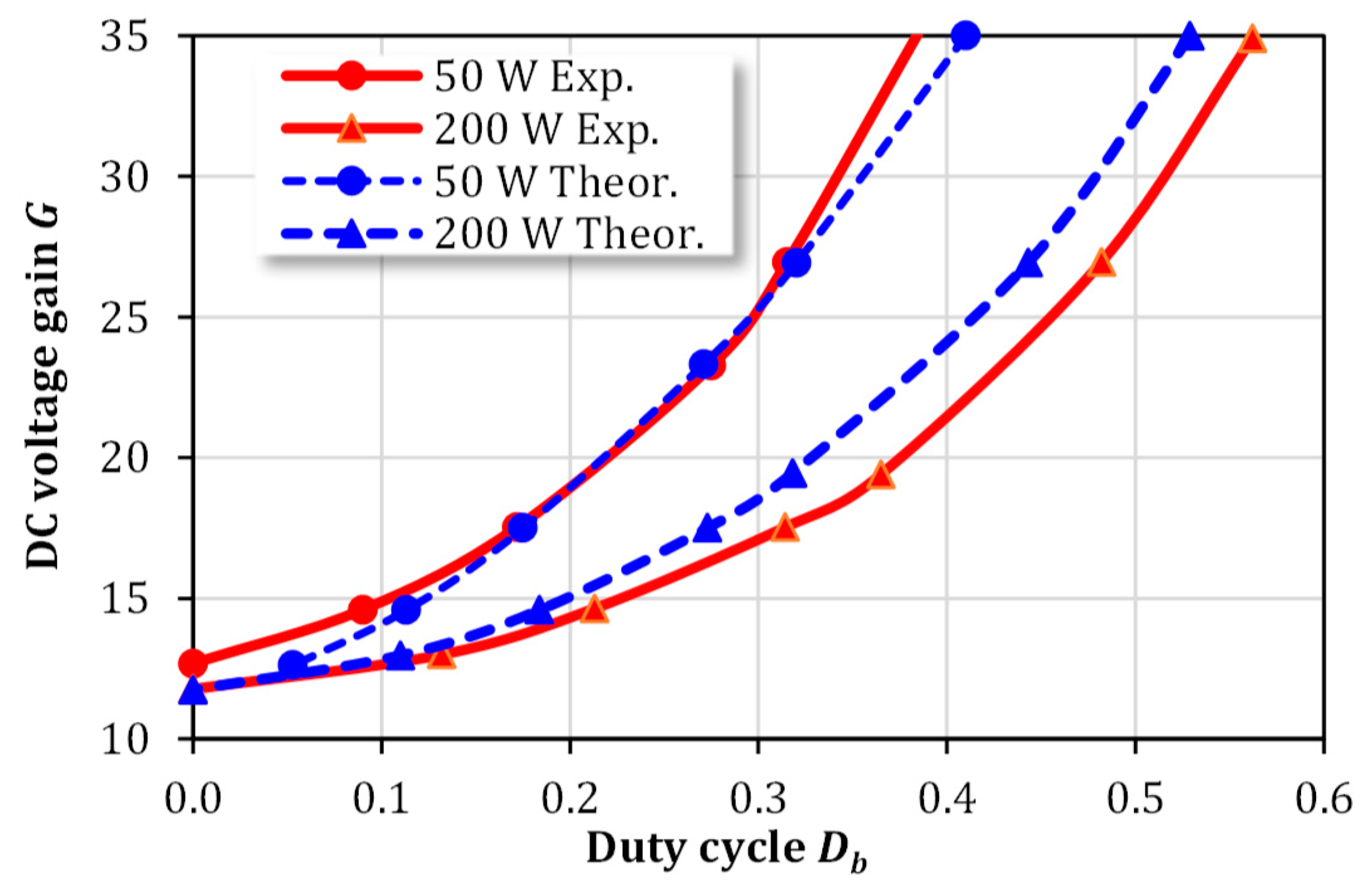
The theoretical and measured conversion gain of the converter as a function in the duty cycle is plotted in Figure 10. The DC voltage gain of the converter equals 12 at Db = 0. Small differences between the theoretical and measured DC voltage gain values occurred due to the influence of power losses. Therefore, at the input power of PIN = 200 W, deviations between the theoretical and measured DC voltage gain values are more significant because the converter experiences higher losses. Evidently, the input power level affects the duty cycle at the same DC voltage gain, for example, at the gain of G = 20: Db = 0.22 at PIN = 50 W and Db = 0.32 at PIN = 200 W.
The input voltage regulation range was measured for the proposed and the baseline topologies. As it was predicted, the baseline converter from [18] features limited input voltage and power regulation range, which is more restricted than was predicted theoretically. The area highlighted with yellow color in Figure 11 describes the input voltage and power range, where the proposed converter can operate and thus achieves superiority over the baseline converter from [18]. Experimental study of the baseline converter shows that it cannot regulate the voltage at duty cycles above some critical value, which drops almost linearly from 0.7 at VIN = 10 V to 0.46 at VIN = 22 V, which corresponds to the limit shown as the green line in Figure 11.
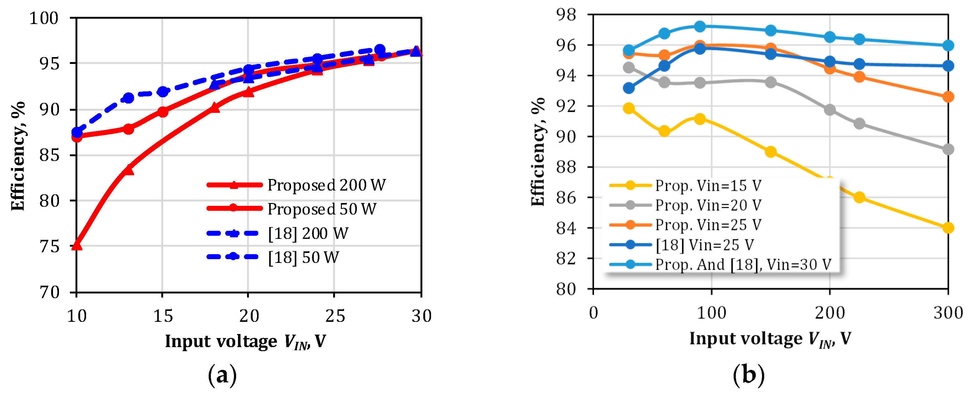
Next, it is essential to examine the efficiency of the converter with different input voltages and power levels. The efficiency measured across the wide input voltage range is shown in Figure 12a. The maximum efficiency of the proposed converter equaled 96% and 96.5% at PIN = 50 W and PIN = 200 W, respectively. These values were achieved when the input voltage was at its maximum level (Db = 0) and the bidirectional switch was turned off. The converter is similar to the traditional SRC and the transformer current had the sinusoidal shape. Accordingly, a full soft-switching was achieved in the converter semiconductors. When the input voltage decreased, the converter activated PWM of the bidirectional switch to boost the transformer voltage up to 350 V. With Db > 0, the converter lost the full soft-switching feature and the converter efficiency decreased together with the input voltage, causing also higher conduction losses. In addition, the efficiency was affected by the operating power due to the change in the quality factor of the resonant tank. The efficiency was also measured versus the input power for different input voltages, as shown in Figure 12b. The efficiency curves are flat across the wide input power range for the input voltages of over 20 V.
Figure 12 also includes several efficiency curves for the baseline converter from [18] to compare it to the proposed converter. It should be noted that the proposed converter features slightly lower efficiencies at higher power, which results from the higher voltage stress of the bidirectional switch in the proposed topology, but higher efficiency at light load, as shown in Figure 12b for the input voltage VIN = 25 V. However, this is an acceptable drawback, considering that the proposed converter can operate in the most critical operating points, that is, at low input voltages and high input currents (cf. Figure 11). For example, the converter from [18] cannot achieve the input power of above 200 W at the input voltage below 18 V, as shown in Figure 12a.
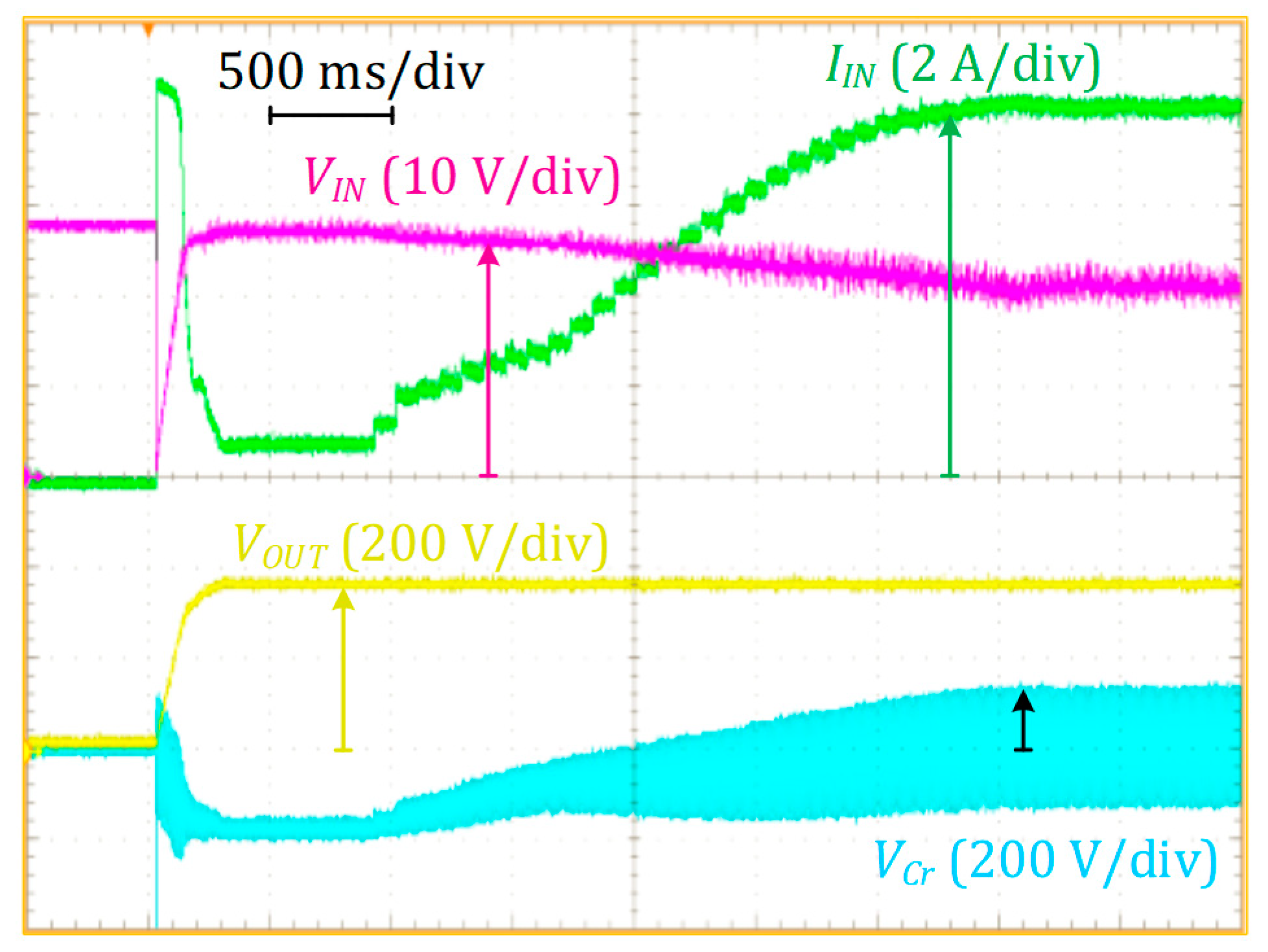
An application-specific study was performed to verify the capability of the proposed converter to perform maximum power point tracking (MPPT). A simplified control approach based on the hill-climbing MPPT algorithm with direct perturbations of the duty cycle was used similar to [21]. For the given converter, operation with a PV module resulted in a reduction in the input voltage when the duty cycle Db was increased. Hence, the direct MPPT can be implemented, avoiding a PI controller. The test was performed using the solar array simulator (SAS) Agilent E4360A as the input power source and electronic DC load Chroma 63204 in the constant voltage mode. The MPPT routine shown in Figure 13 corresponds to the converter operation with a 48-cell monocrystalline-Si PV module Sharp NQ-R258H. When the converter was first connected to the SAS, the current spike appeared due to the charging of the internal capacitances. When the output voltage reached the reference value of 350 V, the DC load started operation and the converter drew a minimum current from the SAS needed to keep the DC load running. After that, the MPPT started with a delay of 0.6 s. The converter reached the maximum power point of the corresponding PV module in 2.5 s. It should be noted that the resonant capacitor experienced an offset of around 200 V caused by start-up transients. Nevertheless, this offset disappeared after several seconds of operation. More importantly, it could be seen that the voltage ripple of the resonant capacitor depended tightly on the input power.

5. Conclusions

This paper presents a new series resonant DC–DC converter with voltage boost capability achieved by using the output-side boost voltage-doubler rectifier. Contrary to the baseline topology, the proposed converter contains the resonant capacitor between the transformer secondary winding and the bidirectional switch. As a result, the proposed converter can operate in the range of low voltages and high currents where the baseline topology cannot operate at all. However, the proposed converter experiences higher voltage stress of the bidirectional switch than that of the baseline counterpart due to the influence of the resonant capacitor voltage ripple, which results in efficiency reduction. Nevertheless, the proposed converter expends the input voltage and power operating range and achieves a peak efficiency of 96.5%. The proposed converter was justified for the module-level PV applications as it is capable of performing the maximum power point tracking and covers a wide voltage range of possible maximum power points that could be observed under shading operation. The main implementation challenge of the proposed converter is related to the design of the isolating transformer. In cost-sensitive applications, it is advisable to integrate the resonant inductor into the transformer, which, however, could result in high proximity losses in the transformer windings. Therefore, future research will be focused on the optimization of the passive components of the converter.

Author Contributions

Conceptualization, A.B. and A.C.; methodology, A.B.; software, A.B.; validation, A.C. and A.B.; formal analysis, A.C. and A.B.; investigation, A.B.; resources, D.V.; data curation, A.C.; writing—original draft preparation, A.C. and A.B.; writing—review and editing, A.C. and D.V.; visualization, A.C. and A.B.; supervision, A.C.; project administration, A.C.; funding acquisition, A.C. All authors have read and agreed to the published version of the manuscript.

Funding

This research was supported in part by the Estonian Research Council grant PSG206, and in part by the Estonian Centre of Excellence in Zero Energy and Resource Efficient Smart Buildings and Districts, ZEBE, grant 2014-2020.4.01.15-0016 funded by the European Regional Development Fund.

Conflicts of Interest

The authors declare no conflict of interest.

Nomenclature

PVPhotovoltaic
SRCSeries resonance converter
ZVSZero voltage switching
LLCInductor-inductor-capacitor resonant converter
PWMPulse width modulation
PSMPhase-shifted modulation
VDRVoltage-doubler rectifier
MOSFETMetal oxide semiconductor field-effect transistor
CrResonant capacitance (F)
frResonant frequency (Hz)
LrResonant inductance (H)
LlkLeakage inductance (H)
LextExternal inductance (H)
VCrThe average voltage of the resonant capacitor (V)
VOUTOutput voltage (V)
LmThe magnetizing inductance of the transformer (H)
nTurns ratio of the transformer
DbCumulative boosting duty cycle
TSWSwitching period (s)
POUTOutput power (W)
ΔVCrThe peak-to-peak ripple of the resonant capacitor voltage
VINInput voltage (V)
COOutput capacitance (F)
ZrResonant impedance (Ω)
ZCSZero current switching
ωrAngular resonant frequency (rad/s)
βLength of the resonant path (rad)
DCMDiscontinuous conduction mode
GnNormalized DC voltage gain
PINmMaximum input power (W)
VINmMaximum input voltage (V)
IINmMaximum input current (A)
PINInput power (W)
MPPTMaximum power point tracking
SASSolar array simulator

References

  1. Dennis, K. Environmentally beneficial electrification: Electricity as the end-use option. Electr. J. 2015, 28, 100–112. [Google Scholar] [CrossRef] [Green Version]
  2. Zhang, G.; Li, Z.; Zhang, B.; Halang, W.A. Power electronics converters: Past, present and future. Renew. Sustain. Energy Rev. 2018, 81, 2028–2044. [Google Scholar] [CrossRef]
  3. Batarseh, I.; Alluhaybi, K. Emerging opportunities in distributed power electronics and battery integration: Setting the stage for an energy storage revolution. IEEE Power Electron. Mag. 2020, 7, 22–32. [Google Scholar] [CrossRef]
  4. Ravyts, S.; Van de Sande, W.; Vecchia, M.D.; den Broeck, G.V.; Duraij, M.; Martinez, W.; Daenen, M.; Driesen, J. Practical considerations for designing reliable DC/DC converters, applied to a BIPV case. Energies 2020, 13, 834. [Google Scholar] [CrossRef] [Green Version]
  5. Cha, H.; Peng, F.Z.; Yoo, D. Z-Source resonant DC-DC converter for wide input voltage and load variation. In Proceedings of the 2010 International Power Electronics Conference—ECCE ASIA, Sapporo, Japan, 21–24 June 2010. [Google Scholar] [CrossRef]
  6. LaBella, T.; York, B.; Hutchens, C.; Lai, J.-S. Dead time optimization through loss analysis of an active-clamp flyback converter utilizing gan devices. In Proceedings of the 2012 IEEE Energy Conversion Congress and Exposition (ECCE), Raleigh, NC, USA, 15–20 September 2012. [Google Scholar] [CrossRef]
  7. Wang, Y.; Liu, R.; Han, F.; Yang, L.; Meng, Z. Soft-Switching DC–DC converter with controllable resonant tank featuring high efficiency and wide voltage gain range. IET Power Electron. 2020, 13, 495–504. [Google Scholar] [CrossRef]
  8. Chub, A.; Vinnikov, D.; Lai, J.-S. Input voltage range extension methods in the series-resonant dc-dc converters. In Proceedings of the 15th Brazilian Power Electronics Conference and 5th IEEE Southern Power Electronics Conference (COBEP/SPEC’2019), Santos, Brazil, 1–4 December 2019. [Google Scholar] [CrossRef]
  9. Kim, J.-W.; Park, M.-H.; Han, J.-K.; Lee, M.; Lai, J.-S. PWM resonant converter with asymmetric modulation for ZVS active voltage doubler rectifier and forced half resonance in PV application. IEEE Trans. Power Electron. 2020, 35, 508–521. [Google Scholar] [CrossRef]
  10. Fei, C.; Lee, F.C.; Li, Q. High-Efficiency high-power-density LLC converter with an integrated planar matrix transformer for high-output current applications. IEEE Trans. Ind. Electron. 2017, 64, 9072–9082. [Google Scholar] [CrossRef]
  11. Nabih, A.; Ahmed, M.; Li, Q.; Lee, F.C. Transient control and soft start-up for 1 MHz LLC converter with wide input voltage range using simplified optimal trajectory control. IEEE J. Emerg. Sel. Top. Power Electron. 2020. [Google Scholar] [CrossRef]
  12. Vandelac, J.-P.; Ziogas, P.D. A DC to DC PWM series resonant converter operated at resonant frequency. IEEE Trans. Ind. Electron. 1988, 35, 451–460. [Google Scholar] [CrossRef]
  13. Kim, E.-H.; Kwon, B.-H. Zero-Voltage- and zero-current-switching full-bridge converter with secondary resonance. IEEE Trans. Ind. Electron. 2010, 57, 1017–1025. [Google Scholar] [CrossRef]
  14. Pahlevani, M.; Pan, S.; Jain, P. A hybrid phase-shift modulation technique for DC/DC converters with a wide range of operating conditions. IEEE Trans. Ind. Electron. 2016, 63, 7498–7510. [Google Scholar] [CrossRef]
  15. Wu, H.; Zhang, J.; Qin, X.; Mu, T.; Xing, Y. Secondary-Side-Regulated soft-switching full-bridge three-port converter based on bridgeless boost rectifier and bidirectional converter for multiple energy interface. IEEE Trans. Power Electron. 2015, 31, 1017–1025. [Google Scholar] [CrossRef]
  16. Son, S.; Montes, O.A.; Junyent-Ferre, A.; Kim, M. High step-up resonant DC/DC converter with balanced capacitor voltage for distributed generation systems. IEEE Trans. Power Electron. 2019, 34, 4375–4387. [Google Scholar] [CrossRef]
  17. Zhao, X.; Chen, C.-W.; Lai, J.-S. A high-efficiency active-boost-rectifier-based converter with a novel double-pulse duty cycle modulation for PV to DC microgrid applications. IEEE Trans. Power Electron. 2019, 34, 7462–7473. [Google Scholar] [CrossRef]
  18. LaBella, T.; Yu, W.; Lai, J.-S.; Senesky, M.; Anderson, D. A Bidirectional-Switch-Based wide-input range high-efficiency isolated resonant converter for photovoltaic applications. IEEE Trans. Power Electron. 2014, 29, 3473–3484. [Google Scholar] [CrossRef]
  19. Zhao, X.; Zhang, L.; Born, R.; Lai, J.-S. A high-efficiency hybrid resonant converter with wide-input regulation for photovoltaic applications. IEEE Trans. Ind. Electron. 2017, 64, 3684–3695. [Google Scholar] [CrossRef]
  20. Vinnikov, D.; Chub, A.; Liivik, E.; Roasto, I. High-Performance quasi-z-source series resonant DC–DC converter for photovoltaic module-level power electronics applications. IEEE Trans. Power Electron. 2017, 32, 3634–3650. [Google Scholar] [CrossRef]
  21. Chub, A.; Zinchenko, D.; Vinnikov, D.; Blinov, A. Three-Port flyback converter for photovoltaic module integration in bipolar dc microgrids. In Proceedings of the 2020 IEEE International Conference on Industrial Technology (ICIT), Buenos Aires, Argentina, 26–28 February 2020. [Google Scholar] [CrossRef]
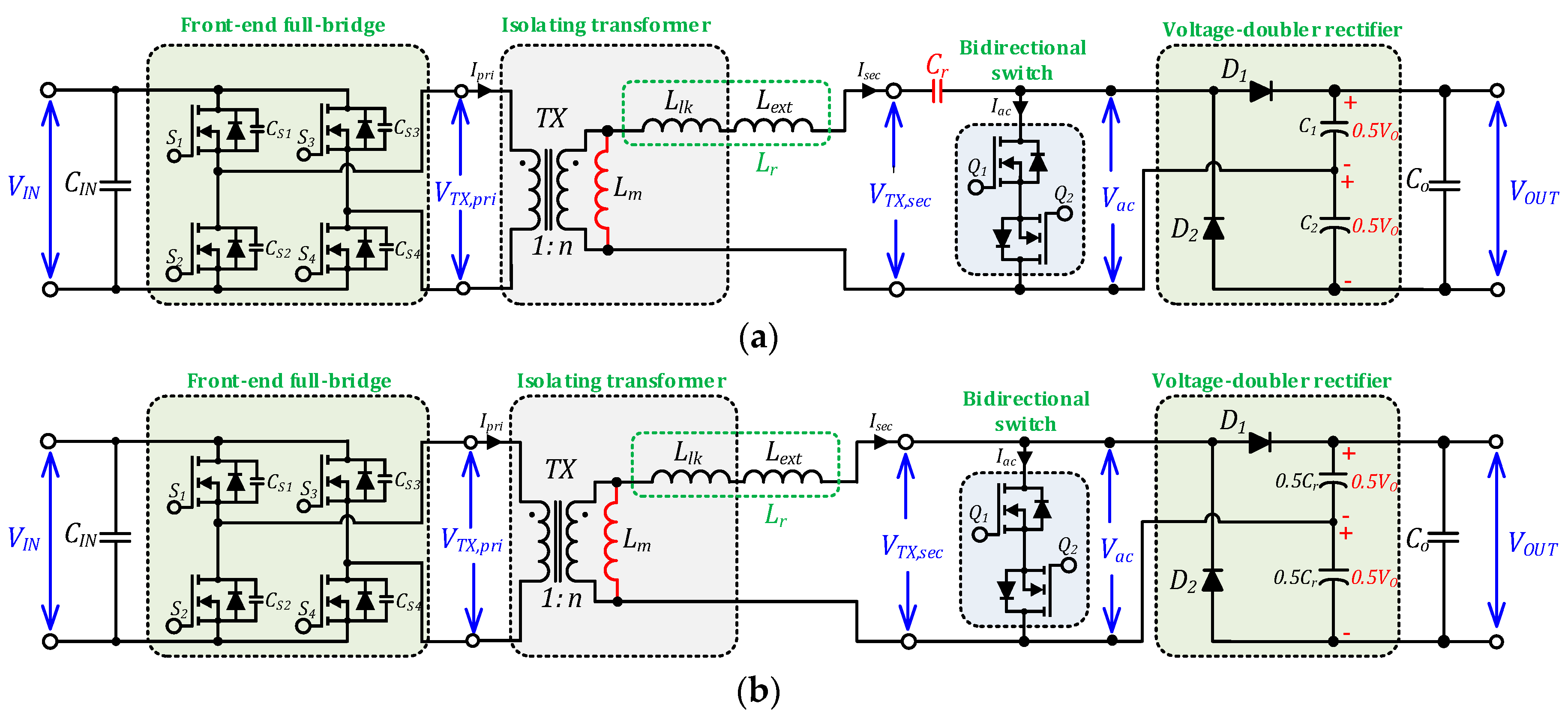
Figure 1. Converter topology of (a) the proposed SRC based on the modified VDR with a bidirectional switch and (b) the SRC presented in [18].
Energies 13 03747 g001
Figure 2. Possible PWM schemes for the bidirectional switch: (a) simple boost PWM and (b) phase-shifted PWM with overlapping signals.
Energies 13 03747 g002
Figure 3. Abnormal operation of the proposed SRC with a boost VDR in the case of PWM scheme from Figure 2b when ΔVCr/2 > nVIN.
Energies 13 03747 g003
Figure 4. Sketch of idealized voltage and current steady-state waveforms of the proposed converter.
Energies 13 03747 g004
Figure 5. The state-plane trajectory of the resonance tank of the proposed SRC.
Energies 13 03747 g005
Figure 6. Equivalent circuit of the resonant tank operation during: (a) Mode I and (b) Mode II.
Energies 13 03747 g006
Figure 7. Comparison between the proposed topology and [18] in terms of (a) the DC voltage at PIN = 300 W and (b) target and feasible input voltage and power ranges for Lr = 100 µH.
Energies 13 03747 g007
Figure 8. Steady-state experimental waveforms of the proposed converter operating at (ac) PIN = 300 W, VIN = 30 V, Db = 0, and (df) PIN = 300 W, VIN = 25 V, Db = 0.215.
Energies 13 03747 g008
Figure 9. Experimental state-plane trajectory for the proposed converter at PIN = 300 W corresponding to (a) the DCX mode and (b) the boost mode.
Energies 13 03747 g009
Figure 10. Calculated and measured DC voltage gain of the converter versus the duty cycle at two input power levels.
Energies 13 03747 g010
Figure 11. Comparison of the experimental limit of the input voltage and power regulation range in relation to the target operating range for the proposed and the baseline SRC topologies.
Energies 13 03747 g011
Figure 12. Comparison of the measured efficiency of the proposed and the baseline converters versus (a) the input voltage at two power levels and (b) the input power at different input voltage levels.
Energies 13 03747 g012
Figure 13. Experimental MPPT routine.
Energies 13 03747 g013
Table 1. Setup parameters and components.
ParameterSymbolValue
Input voltage rangeVIN10:30 V
Input-side capacitorCIN150 µF
Transformer leakage inductance Llk4 µH
Transformer magnetizing inductanceLm1.3 mH
External inductorLext92.5 µH
Resonance capacitorCr30 nF, metal film
Voltage-doubler capacitorsC1, C2150 µF, electrolytic
Output-side capacitorsCo150 µF
Output voltageVOUT350 V
Switching frequencyFs95 kHz
ComponentsSymbolPart Number
Primary-side switchesS1, S2, S3, S4FDMS86180
Bidirectional switch Q1, Q2SCT2120AF
Output-side diodesD1, D2C3D02060E