Article

Multi-Objective Optimization of the Gate Driver Parameters in a SiC-Based DC-DC Converter for Electric Vehicles

1
Department of Electrical and Electronic Engineering (DIEE), University of Cagliari (UniCa), 09123 Cagliari, Italy
2
Centre for Industrial Electronics, University of Southern Denmark, 6400 Sønderborg, Denmark
*
Author to whom correspondence should be addressed.
Energies 2020, 13(14), 3720; https://doi.org/10.3390/en13143720
Submission received: 15 June 2020 / Revised: 10 July 2020 / Accepted: 16 July 2020 / Published: 20 July 2020

Abstract

:
DC-DC converters are being used for power management and battery charging in electric vehicles (EVs). To further the role of EVs in the market, more efficient power electronic converters are needed. Wide band gap (WBG) devices such as silicon carbide (SiC) provide higher frequency and lower power loss, however, their high di/dt and dv/dt transients result in higher electromagnetic interference (EMI). On the other hand, some gate driver parameters such as gate resistor ( R G ) have a contradictory effect on efficiency ( η ) and EMI. The idea of this paper is to investigate the values of these parameters using a multi-objective optimization method to optimize η and EMI at the same time. To this aim, first, the effect of high and low side R G on η and EMI in the half-bridge configuration is studied. Then, the objective functions of the optimization problem are obtained using a numerical regression method on the basis of the experimental tests. Then, the values of the gate resistors are obtained by solving the multi-objective optimization problem. Finally, η and EMI of the converter in the optimum gate resistor design are compared to those in the conventional design to validate the effectiveness of the proposed design approach.

1. Introduction

One of the causes of global warming and air pollution is the gas propulsion in conventional vehicles (CVs). Hybrid, fuel cell, electric, and plug-in vehicles, as well as the vehicle-to-grid (V2G) concept are alternatives for CVs in which the fossil fuels can be replaced by green renewable energies. Fossil fuels are a serious threat to Earth, are diminishing, and are becoming increasingly expensive [1]. Plug-in hybrid electric vehicles (PHEVs), for instance, are under development to be superseded in the market eventually [2]. Besides the energy storage systems, such as the batteries, the ultra-capacitors, and the fuel cells, which are an important field of research to advance the PHEVs [3], the efficient compact converters are also absolutely essential to push the PHEVs forward [4,5,6].
The AC-DC-DC battery chargers, the DC-DC bidirectional converters for the power management, and the DC-AC traction inverters, which are being used in the PHEVs [7,8], benefit from the high efficiency and the high frequency capability of the new wide band gap (WBG) devices such as silicon carbide (SiC) [9,10]. In [11,12,13,14], some SiC-based converters in automotive applications are discussed and their superiority over Silicon (Si) devices has been presented.
The most important figure of merit (FOM) of the semiconductor devices is R DS ON × Q G where R DS ON and Q G are the drain-source ON resistance and the gate charge, respectively. Lower R DS ON results in lower conduction loss ( P Cond ) while lower Q G leads to a faster switching transient and consequently lower switching loss ( P SW ). A faster switching transient of SiC devices provides higher efficiency, however sharp voltage/current transients (di/dt and dv/dt) cause high frequency noises and deteriorate the electromagnetic compatibility (EMC) performance of the converter [15].
Gate driver design is a critical task from the point of view of efficiency ( η ) and EMC. If we consider an optimization problem in which the η and the electromagnetic interference (EMI) are the objectives, in some cases, it is directly possible to optimize both objectives. For example, a gate driver design with a novel topology [16] or a PCB design with an innovative device placement [17,18,19] can reduce parasitics, ringing, and improve EMI without deteriorating the switching speed. Lower ringing results in lower “ringing losses” [20] and consequently improve η as well. In some other cases, however, such as gate resistor design, the value of gate resistor ( R G ) has a conflictive effect on the objectives of the optimization problem. For instance, a higher value of R G suppresses ringing so that improves EMI while it causes a slower switching transient, higher switching loss, and therefore leads to lower efficiency [15]. Noticeably, in this case, the switching loss raise is dominant compared to the ringing loss reduction. As a result, for parameterization of R G , “multi-objective optimization” can be proposed to optimize the both objectives ( η and EMI) at the same time.
In [21], both η (total switching loss) and EMI (current overshoot plus voltage overshoot) of a GaN-based inductive battery charging system are considered in an optimization problem and the R G is parameterized. The methodology is “numeric” where the amount of the both total switching loss and current/voltage overshoot are obtained by experimental tests with five values of R G (5, 10, 15, 22.5, 27.5 Ω ). Then, an objective function, total power losses × (%V_overshoot + %I_overshoot), is defined as a function of the value of R G . Finally, R G = 10 Ω is selected for the gate resistor design in order to minimize the defined objective function.
In [22], the idea is the parameterization of both the high side (HS) and low side (LS) gate resistors ( R G HS and R G LS ) in a GaN-based one leg inverter by solving a multi-objective optimization problem. The objective functions are the efficiency and the EMI level of the circuit. The methodology is numeric where the amount of the objective functions are obtained on the base of the OrCAD PSpice simulations for 5 × 5 = 25 tests with different values of R G HS and R G LS : five values for each resistor where the objective functions are η = f 1 ( R G HS ,   R G LS ) and EMI = f 2 ( R G HS ,   R G LS ) . Unlike [21], in [22] the mathematical expression of the objective functions is obtained by the use of a regression method. Then, solving a multi-objective optimization problem, the “Pareto front” of the problem is obtained. Finally, the values of R G HS and R G LS are selected corresponding to one of the optimum points in the Pareto front.
In this paper the idea is the same as that of [22], however, the half-bridge configuration is more completed where there are four gate resistors to be studied instead of two: turn-ON HS gate resistor ( R G HS ON ), turn-OFF HS gate resistor ( R G HS OFF ), turn-ON LS gate resistor ( R G LS ON ), and turn-OFF LS gate resistor ( R G LS OFF ). Moreover, the power electronic converter is a SiC-based half-bridge DC-DC converter for the application of electric vehicles (EVs). Unlike [22], where the evaluation of the proposed method is only on the base of the OrCAD PSpice simulations, here, the proposed method is evaluated by performing the experimental tests. In addition, in this paper, the half-bridge configuration is analyzed by addressing Miller effect crosstalk, which is a hot topic for the WBG devices such as SiC, as it is explained later in this section. The detailed methodology is presented in the next section.
Here, it is worthy to review some other state-of-the-art literature concerning the gate driver design in general and for SiC-based converters in particular. In the next section, the relevance of the following reviewed literature with the motivations of this paper is shown.
In [23], a cost-effective robust active gate driver (AGD) is proposed for IGBTs. The AGDs unlike the conventional gate drivers (CGDs), get feedback from the output voltage/current variables of the switching device in order to control the transient behaviors (dv/dt and di/dt). In this way, both switching loss and EMI can be reduced. To this aim, the desirable transient voltage/current rating should be studied in an “analytical” way. The gate driver in [23] offers robustness for the junction temperature and the load variations. In [24], a digitally programmable AGD is proposed. While the control parameters of an analog AGD are fixed, the proposed AGD can be programmed digitally to be fitted with the “parasitic” inductances/capacitances after implementation of the converter.
An important subject of the recent works on SiC devices is to suppress “Miller effect crosstalk” in half-bridge configuration [16,25,26]. Miller effect crosstalk happens in half-bridge configuration when turning-ON and turning-OFF of one switching device generates gate-source voltage spikes on its complementary switching device [25]. In [26], three methods of Miller effect crosstalk suppression for Si devices are stated: (1) add additional capacitance between gate–source terminals to shunt the Miller current, (2) apply a negative-biased turn-OFF gate voltage, and (3) active Miller clamping. However, due to the intrinsic characteristics of SiC, such as low threshold gate voltage, low maximum allowable negative gate voltage, and large internal gate resistance, Miller effect crosstalk is a serious issue and the conventional design approaches are not optimum. So that, additional gate driver circuits are proposed in [26] for an active gate impedance/voltage control. In [16], apart from proposing a new gate driver circuitry to suppress Miller effect crosstalk, the effect of the parasitic inductances is discussed. Therefore, in order to higher suppression of Miller effect crosstalk, beside the active gate control, there are PCB considerations to minimize the parasitic inductances as well.
The rest of the paper is organized as follow. In Section 2, the configuration of the converter and the proposed design approach are presented in detail. In Section 3, the experimental results and the extended discussion are presented. Finally, in Section 4, the conclusions are presented.

2. Multi-Objective Optimization of the Gate Driver Parameters

In this section, the configuration of the SiC-based DC-DC converter and its gate drivers are presented. Then, the method of finding the objective (regression) functions is discussed where the dependency of the efficiency and the conducted EMI to the gate resistors is studied. In this part, it is explained that how the gate resistor pairs can be selected on the basis of the Miller effect crosstalk suppression. At the end, the multi-objective optimization problem is solved where a Pareto front is achieved in order to find the optimal design points.
Figure 1 and Figure 2 present the configuration of the SiC-based DC-DC converter and the gate drivers respectively. In Figure 1, a half-bridge bidirectional boost converter is shown as a typical topology for power management between the battery and the traction inverter in the application of EVs. More about the operation modes and the power stage design of the half-bridge bidirectional boost converter as the power management module in EVs can be found in [27]. Since the converter is bidirectional, there are two SiC MOSFETs as the HS/LS switches. Moreover, because of the characteristic of the body diode of the SiC MOSFETs, that are very similar to those of a typical anti-parallel diode, there is no need to make use of the anti-parallel diodes in the SiC-based converter [28]. In Figure 1, the parasitic elements of the circuit are depicted as well: the loop parasitic inductances L dp 1 , L dp 2 , L dp 2 , and L sp 2 where d stands for drain, s stands for source, and p stands for parasitic; moreover, the coupled heat-sink parasitic capacitances C hp 1 , C hp 1 , and C hp 1 where h stands for heat-sink. The fast transition voltage ( dV DS dt ) and current ( dI D dt ) of the HS/LS switches, in line with the parasitics of the circuit cause a conducted EMI current which passes through the parasitic capacitances ( C hp 1 , C hp 1 , and C hp 1 ) to the heat-sink and then to the power ground (PG). The maximum amplitude of this ground current in μAdB ( I ^ GR ) can be considered as the EMI level of the converter [29].
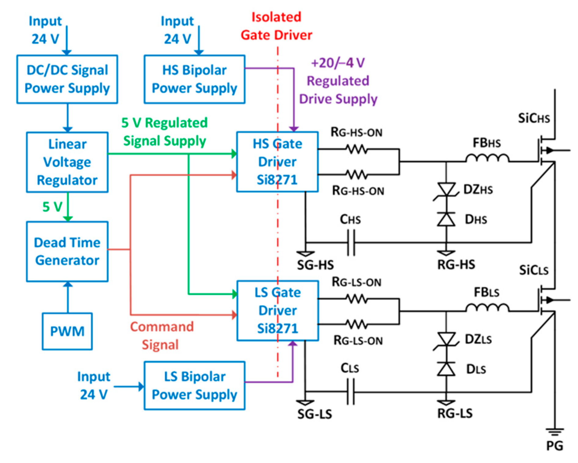
As can be seen in Figure 2, two gate drivers with the same configuration are considered for the HS/LS SiC switching devices. Each gate driver has its own turn-ON and turn-OFF paths and the corresponding gate resistors. So that, there are four gate resistors in the circuit as: R G HS ON , R G HS OFF , R G LS ON , and R G LS OFF . The clamp diodes, DZ HS / DZ LS and D HS / D LS , are used to mitigate the overshoot of the HS/LS gate-source voltages. In order to damp the high frequency ringing of the LC gate driver parasitics, the ferrite beads, FB HS and FB LS , are used with an impedance of Z = 220 Ω at 100 MHz. The gate driver ICs are Si8271 manufactured by Silicon Labs. High integration, low propagation delay, small installed size, flexibility, and cost effectiveness make Si8271 ideal for SiC or GaN devices [30]. In this paper, two gate driver ICs are used separately as the single gate drivers for each switching devices in order to increase the reliability of the gate driver design. The topology of the gate driver ICs is totem-pole with a fully isolated configuration, using bipolar power supplies (+20/−4 V) to drive the gate-source voltage ( V GS ) of the switching devices.
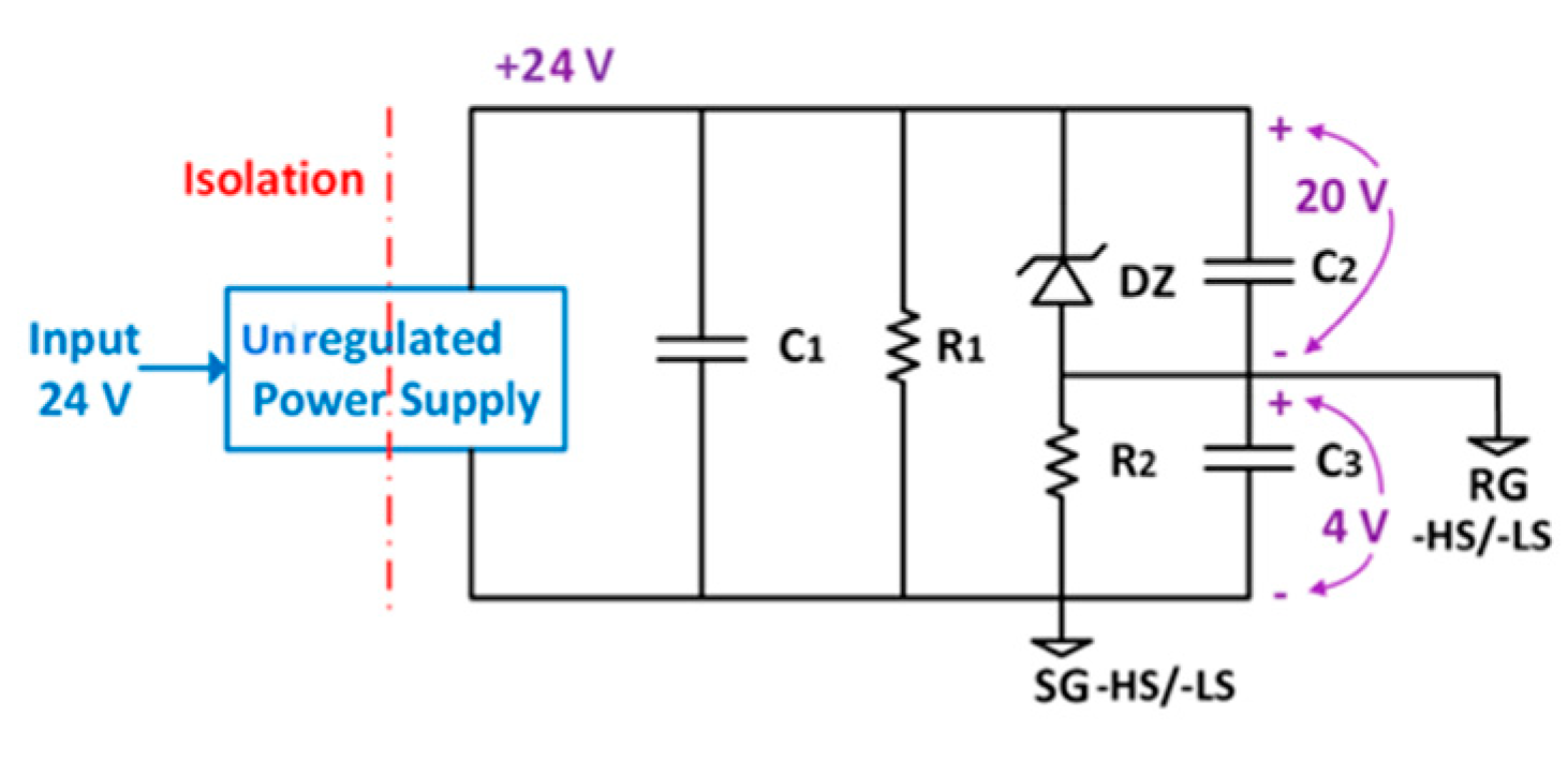
The bipolar power supply circuits are identical for the both gate drivers (Figure 3). The HS/LS indices are used to refer to the HS/LS bipolar power supplies respectively. The Zener diode ( DZ ) in series with the resistor R 2 realize the ON/OFF gate-source voltages of +20/−4 V. The connection point between DZ and R 2 are the reference ground (RG) for the switching devices in both Figure 2 and Figure 3. The low voltage signal ground for the gate drivers is indicated with SG as well. For the bipolar power supply design, the reference is the GaN gate driver design application note [31], while the values of circuit parameters are suitably modified for the SiC switching device.
In order to find the objective functions, first it is needed to define the optimization problem as below:
minimize   f 1 ( x ) ,   f 2 ( x )
x R ,   R = { R G HS ON , R G HS OFF ,   R G LS ON ,   R G LS OFF }
where f 1 ( x ) is the efficiency of the converter with a negative mathematical sign (− η ). In another words, finding the minimum value of − η , is in fact finding the maximum value of η . Moreover, f 2 ( x ) is the EMI level of the converter ( I ^ GR ).
The objective functions can be obtained in a (1) analytical or in a (2) numerical way. In the analytical way, a circuit analysis is needed where all parameters of the circuit such as parasitics and the circuit model of the switching devices are known. In the numerical way, the circuit is considered as a black-box system where the inputs of the system are the gate resistors and the output of the system are the efficiency and the EMI level. Then, some experiments should be performed to obtain a number of input–output pairs of the system. To perform the experiments, the circuit is already designed and implemented. Therefore, while the final goal is to modify the gate resistors, the other parameters of the circuit such as parasitic inductances/capacitances are already set up. It means that the gate resistor optimization is fitted to the other parameters of the circuit. In this sense, the approach of this paper has the same advantage as that of the [24], as discussed in the first section, where the parasitic parameters of the circuit are considered in the final design/control of the gate driver. Once the input–output pairs are obtained, the objective functions can be estimated by applying a regression method on the input–output pairs. As a result, the objective functions can be named regression functions as well. In this study, the numerical way is considered.
The number of experiments, which can be performed in order to obtain the input–output pairs, are technically limited. If we consider all four gate resistors as the inputs of the system and if we want to perform the experiments with, for example, five different values for each resistor, we need 54 = 625 experiments to map the input–output pairs in a five-dimension space (four independent variables and one output). Such a high number of experiments is technically out of reach. To solve this problem, we can consider a two-phase optimization approach in which only two gate resistors are considered as the input of the system for each phase. In this way, the number of the experiments will be reduced by 52 = 25 for each phase of the optimization approach to map the input–output pairs in a three-dimension space (two independent variables and one output).
Now, the question is that which two gate resistors should be selected for each phase of the optimization approach. Technically, there are three options: { R G HS ON , R G HS OFF } for one phase and { R G LS ON , R G LS OFF } for the other phase, { R G HS ON , R G LS ON } for one phase and { R G HS OFF , R G LS OFF } for the other phase, and { R G HS OFF , R G LS ON } for one phase and { R G HS ON , R G LS OFF } for the other phase. Among these three options, the last one is selected in this study based on Miller effect crosstalk between the HS/LS switches in the half-bridge configuration. In the first section, the Miller effect crosstalk has been introduced. In [32], based on the circuit analysis of the half-bridge configuration with respect to the Miller effect crosstalk, it is explained how the gate resistors R G HS OFF and R G LS ON should be designed coordinated to each other to minimize the Miller effect crosstalk loss during the turn-ON process of the LS switch and evade a spurious turn-ON of the HS switch. Relatively, the gate resistor pairs, R G HS ON and R G LS OFF should be designed accordingly to minimize the Miller effect crosstalk loss during the turn-ON process of the HS switch and evade a spurious turn-ON of the LS switch. In this paper, only one phase of the optimization approach is studied where the inputs of the system are the gate resistor pairs R G HS OFF and R G LS ON . The second phase of the optimization approach, where the inputs of the system are the gate resistor pairs R G HS ON and R G LS OFF , is considered as the future work. As a result, we can rewrite the multi-objective optimization problem of the Equation (1) as below:
minimize η = f 1 ( x ) ,   I ^ GR = f 2 ( x ) x R ,   R = { R G HS OFF ,   R G LS ON }
Details about the experiments are discussed in the next section. In the next step, when the experiment results are available and the input–output pairs are obtained, a regression method should be applied on the input–output pairs to estimate the objective functions f 1 and f 2 . From now, the objective functions can be called regression functions as well. Since there are two independent variables, R G HS OFF and R G LS ON ; a “multivariate” regression method should be performed. In this paper, the fitlm solver from the Statistic and Machine Learning Toolbox of MATLAB is used for which, the model of the regression function should be specified. To this aim, a “quadratic polynomial” model is selected for the objective functions to minimize the regression modelling error:
f 1 ( x ) = a 0 + a 1 x 1 + a 2 x 2 + a 3 x 1 x 2 + a 4 x 1 2 + a 5 x 2 2 f 2 ( x ) = b 0 + b 1 x 1 + b 2 x 2 + b 3 x 1 x 2 + b 4 x 1 2 + b 5 x 2 2 x 1 = R G HS OFF ,   x 2 = R G LS ON
where the purpose of the regression step is to estimate the coefficients of the models: a i and b i for i = {1, 2, 3, 4, 5}.
In the next step, a multi-objective optimization solver should be used, using the regression functions, to solve the optimization problem of Equation (2), considering a boundary for the independent variables as:
R = { R G HS OFF ,   R G LS ON } ,   R bound = [ R min ,   R max ]
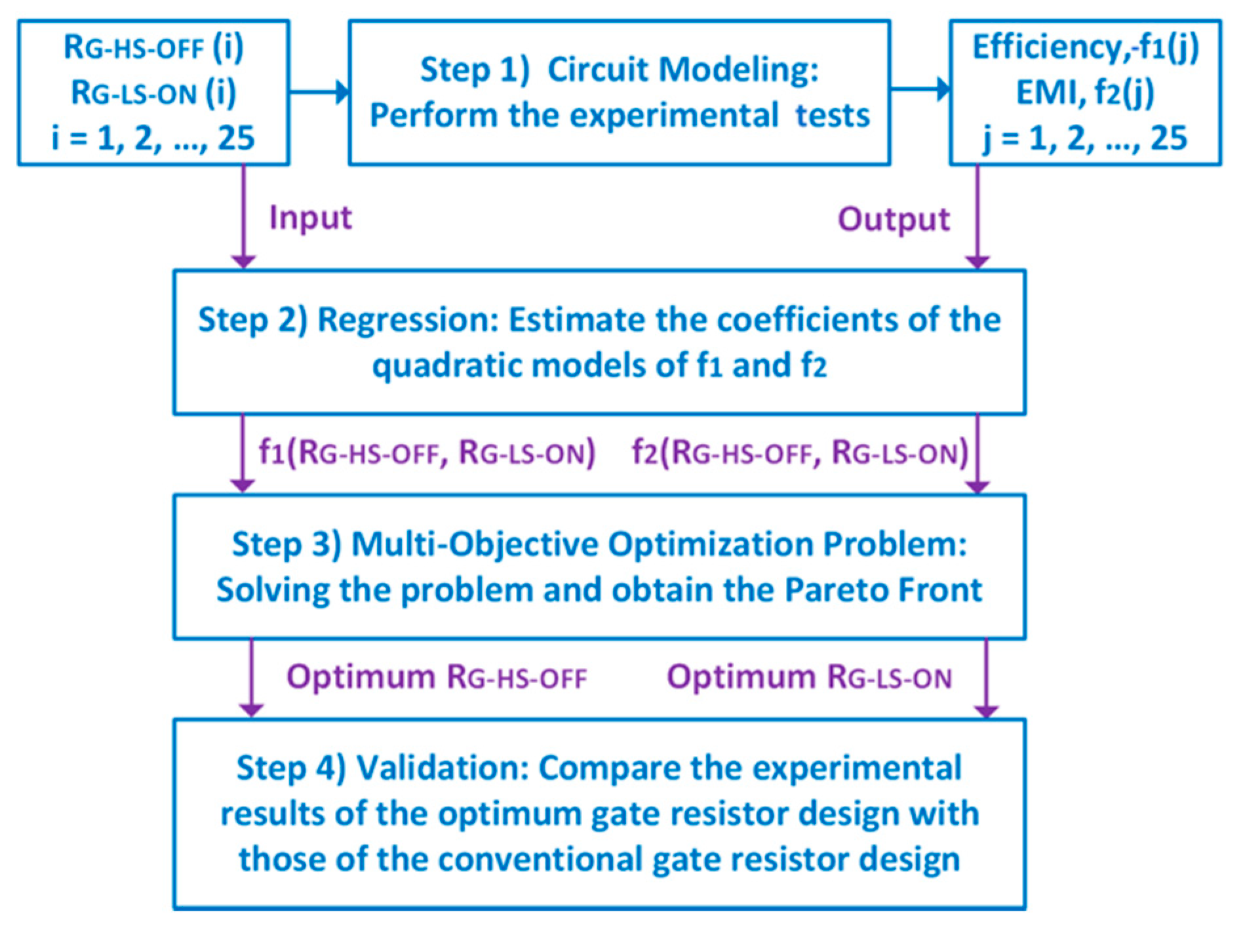
In this paper, the gamultiobj non-linear multi-objective optimization solver from the Optimization Toolbox of MATLAB is used. This multi-objective optimization solver plots a Pareto front where there are optimum points in a two-dimension space, represented the two objective functions. These points indicate the optimum value choices for the both objective functions. Then, it is the designer’s decision to select one optimum point among all the suggestions. Obviously, the higher efficiency costs a higher EMI level and vice versa. Finally, the efficiency and the EMI level in the case of the optimum design should be compared with those of a conventional design to validate the effectiveness of the proposed approach. All the steps are shown in the flowchart of Figure 4.

3. Experimental Results and Discussion

Here, at the first subsection, the test set-up, the measurement tools, and the test conditions are presented. Then, the 25 experiments are performed for different values of the gate resistors to obtain the input–output pairs of the system. In the second subsection, the regression functions are estimated and plotted, using the experimental results of the first subsection. In the third subsection, the multi-objective optimization problem is solved, the Pareto front is plotted, and an optimum point is selected. In the fourth subsection, the set-up is tested, mounting the corresponding gate resistors of the selected optimum point of the third subsection. Then, the results are compared with those of a conventional gate resistor design. In the conventional gate resistor design, the gate resistor values are selected based on the application note suggestions for the SiC devices. In the fifth subsection, the experimental results are discussed in depth and the future works are suggested.

3.1. Test Set-up, Measurement Tools, and Test Conditions

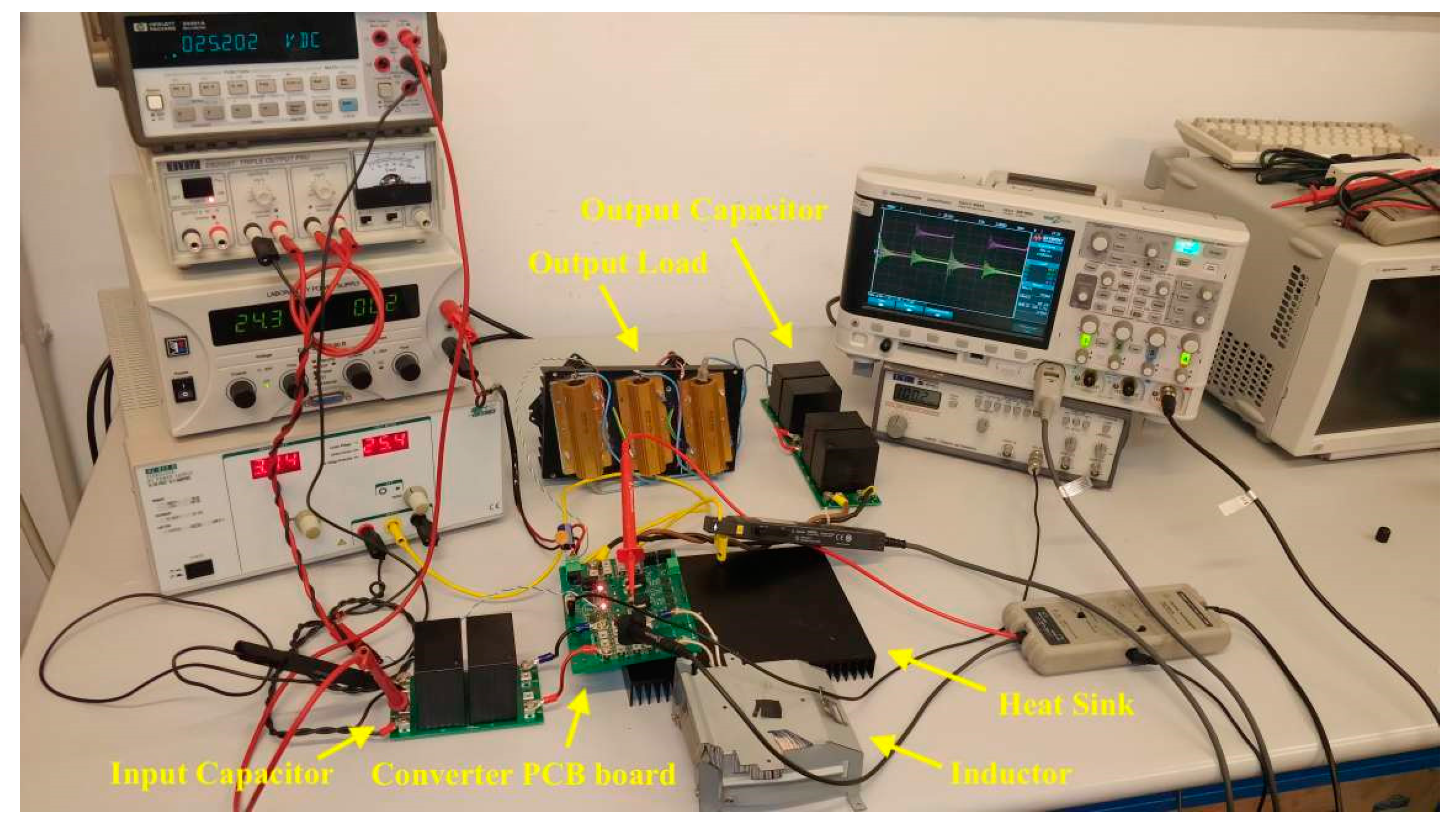
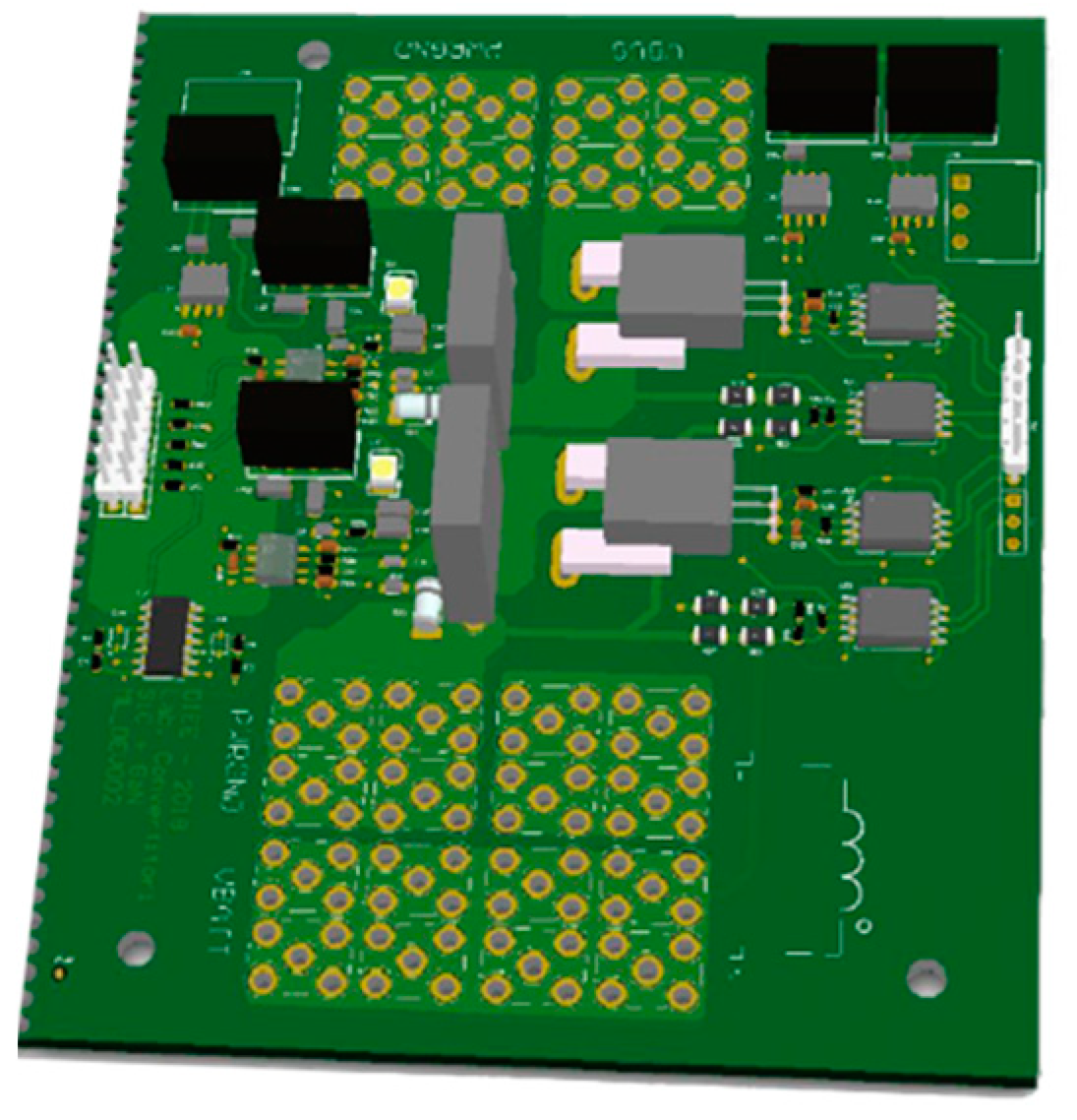
In Figure 5, the set-up of the converter and the measurement tools are shown. In Figure 6, the 3D PCB board of the converter, designed by Altium, is depicted.
The specifications of the power stage, of the gate drivers, and of the measurement tools are presented in Table 1, Table 2 and Table 3 respectively. The conventional design refers to the selection of the gate resistor values based on the suggestion of the application notes for SiC [28,29,30,31,32]. The conventional design gate resistor values are:
R G LS ON = R G LS ON = 4.7   Ω ,   R G HS OFF = R G LS OFF = 2.2   Ω
It is considered 52 = 25 experimental tests, five different values for each of R G HS OFF and R G LS ON , while R G LS ON and R G LS OFF remain unchanged. The five different test values are selected as:
R G HS OFF ,   R G LS ON = { 1   Ω ,   5   Ω ,   10   Ω ,   20   Ω ,   50   Ω }
For each of the 25 experiments (indicated with j in Figure 4), the corresponding gate resistors (indicated with i in Figure 4) are mounted on the PCB board. Since the aim of this work is just to study the proposed multi-objective optimization approach, the tests are performed at a low input voltage and a low output power to evade the risk of damaging the circuit. The test conditions are summarized in Table 4. The output load consists of three resistances, 10 Ω and 150 W each, connected in series and mounted on a heat-sink (Figure 5). Each test should be performed when the switching devices reach their steady-state temperature in order to keep the test condition equal for all the experiments in the term of R DS ON and the corresponding P Cond . The ambient temperature also should be kept as constant as possible for all the tests as the resistance of the load, the corresponding operation point, and the total loss are dependent to the ambient temperature.

3.2. Regression Functions

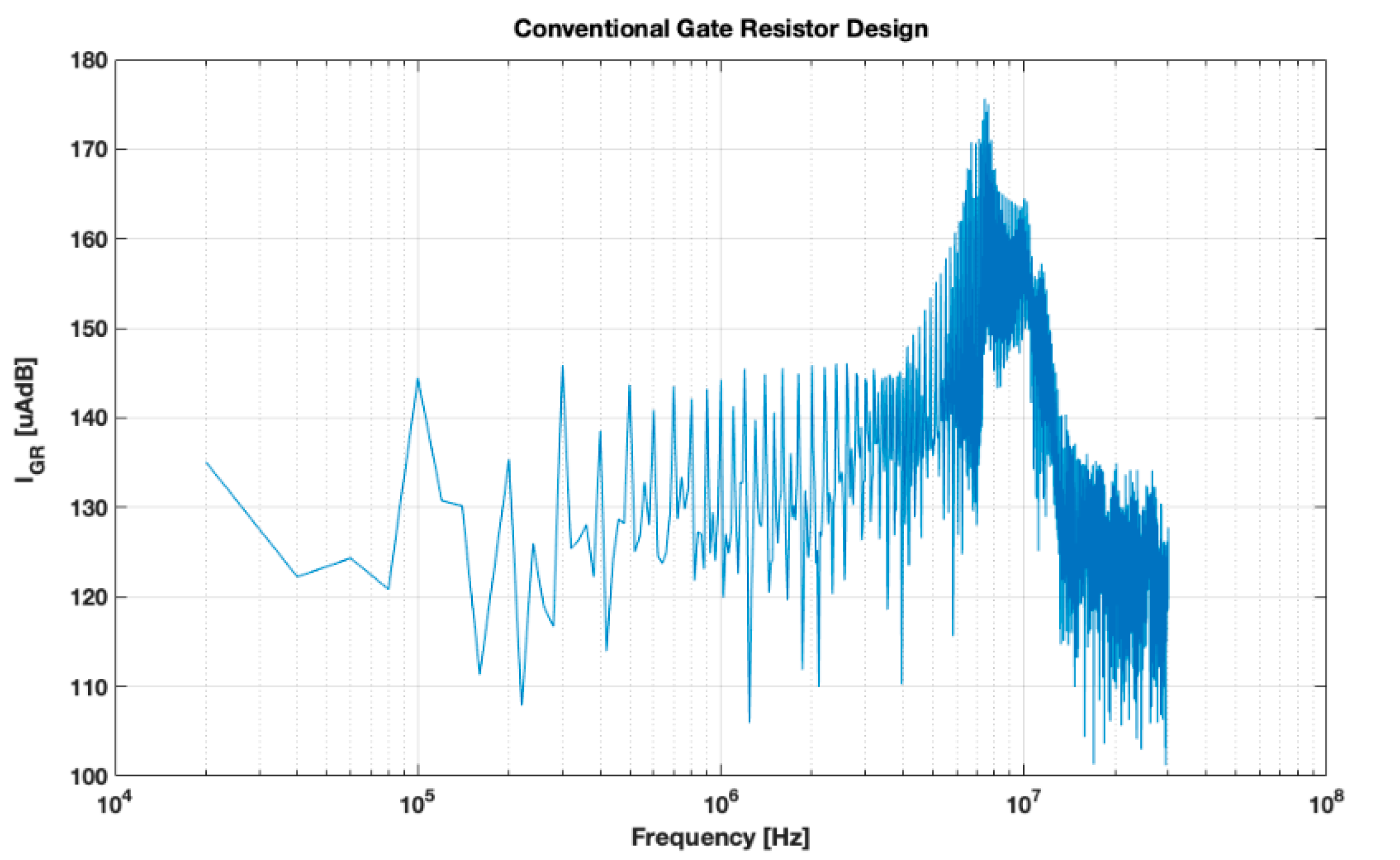
For each experiment, there are two independent variables, R G HS OFF and R G LS ON , and two dependent variables, namely the efficiency and the EMI level. The efficiency is the overall efficiency of the converter, which is obtained by measuring the input/output current/voltage of the converter. The EMI level is obtained by measuring the heat-sink ground current of the converter, applying Fourier transform, plotting the “spectra” diagram, and considering the maximum amplitude of the spectra diagram in μAdB ( I ^ GR ) as the EMI level. The spectra diagram of the ground current for the case of the conventional gate resistor design is shown in Figure 7.
Once all the 25 input–output pairs are obtained from the experiments, the fitlm solver from the Statistic and Machine Learning Toolbox of MATLAB can be applied to estimate the coefficients of the regression functions as it is described in Equations (3). In Figure 8, the 3D mesh plots of the regression functions are shown.

3.3. Multi-Objective Optimization Problem and Pareto Front

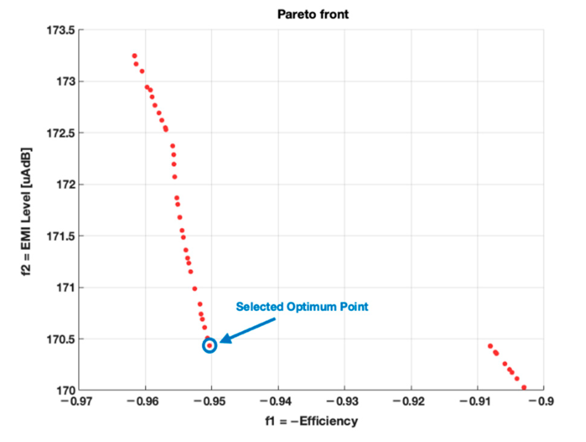
In this step, the multi-objective optimization problem of Equation (2) should be solved. The boundary of the independent variables, as described in Equation (4), is selected as R bound = [1 Ω , 50 Ω ]. The multi-objective optimization problem is solved using the gamultiobj non-linear multi-objective optimization solver from the Optimization Toolbox of MATLAB. The solver provides the Pareto front as well, where a number of optimum points are achieved (Figure 9). Then, it is the designer’s decision to choose the desired optimum point that is more matched with the design goals. In this paper, the indicated optimal point, as it can be seen in Figure 9, is selected. The expected efficiency and EMI level of the selected optimum point are 0.9504 and 170.4 μAdB, respectively. The values of the corresponding independent variables of the selected optimum point are R G HS OFF = 1.5 Ω and R G LS ON = 14 Ω as well.

3.4. Optimum Gate Resistor Design

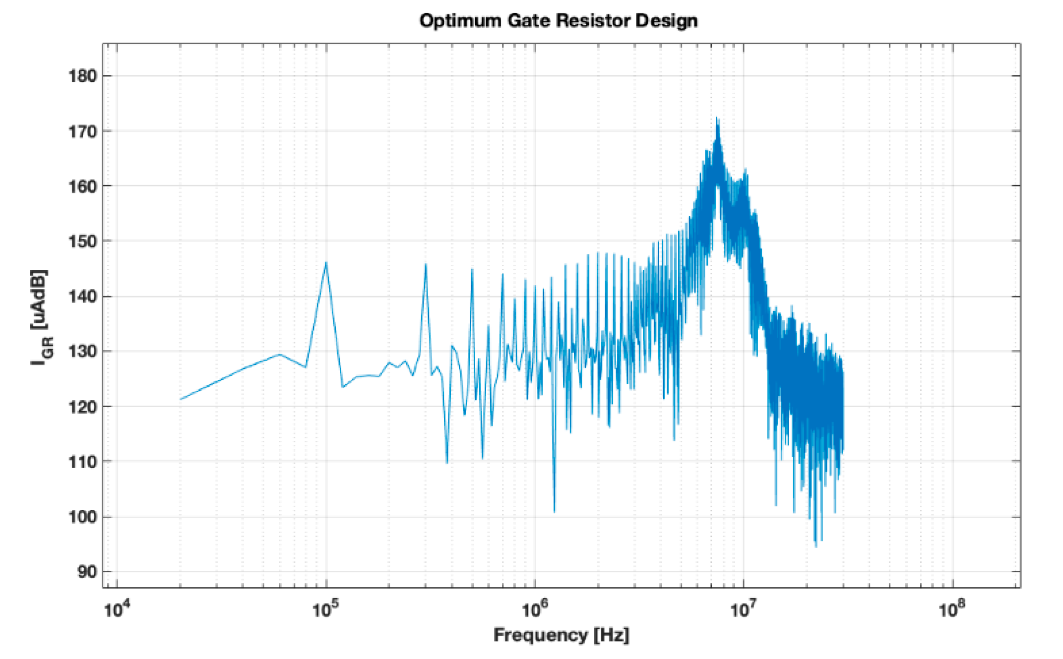
Here, the optimum gate resistors are mounted, and the measurements are performed to obtain the efficiency and the EMI level. In Table 5, the experimental results are compared between the two design cases: conventional and optimum. An improvement of 0.986% for the efficiency and an improvement of 1.84% for the EMI level are achieved in the case of the optimum design compared to the conventional design. It should be noticed that the experimental results of the optimum design (0.9624 of efficiency and 172.33 μAdB of EMI level) are not equal to those of the selected optimum point in Pareto front (0.9504 of efficiency and 170.4 μAdB of EMI level) as there is always a total error resulting from measuring, regression, optimization problem solving, etc. in the design procedure (1.24% for efficiency and 1.12% for EMI level). In addition, the spectra diagram of the optimum gate resistor design is shown in Figure 10. The maximum amplitude of I ^ GR has a corresponding frequency of 7.4 MHz, the same as that of the conventional design of Figure 7.

3.5. Discussion and Future Works

In this paper, a multi-objective optimization approach to design the gate resistors are proposed. There are some points that should be highlighted. First, the aim of this work is just to study the proposed approach and validate its superiority respect to the conventional design. So, while the efficiency and the EMI level of the implemented converter are not competitive with those of a commercial product, the effectiveness of the proposed gate resistor design can be still validated. For the same reason, the proposed design approach is studied at low voltage/power respect to the rating values in order to evade putting high stresses on the implemented converter. Second, the proposed design approach adds no cost and complexity to the circuit. Third, even if the case study in this paper is a SiC-based DC-DC converter in the application of EV, the proposed gate resistor design approach can be applied for any power electronic converter with a half-bridge configuration. Fourth, as the proposed design approach is applied after the implementation of the converter, the characteristics of the circuit, especially the parasitics related to the PCB design, have their effect on the values of the optimum gate resistors. On the contrary, in a conventional gate resistor design, the mentioned characteristics of the circuit, cannot be seen in the design approach. Fifth, the efficiency and the EMI level are improved, however, the EMI level improvement is not very satisfying. To understand the reason of the low EMI level improvement, the drain-source voltage of the LS switch ( V DS LS ) and the ground current ( I GR ) should be studied. To this aim, they are presented in Figure 11. As can be seen, the overshoots of the signals are slightly lower in the case of the optimum design.
In some EMI studies for power electronic converters, such as those of [33,34], the ringing of the node voltage ( V N ) in the half-bridge configuration (see Figure 1), which is practically equal to V DS LS , is considered as the factor of EMI level evaluation. With respect to the gate resistors, R G HS ON can control the ringing of V N , while in this paper, where only one of the gate resistor pairs ( R G HS OFF and R G LS ON ) is optimized, R G HS ON is remained unchanged. In some other EMI studies for power electronic converters, such as those of [29] and this paper, the maximum amplitude of the heat-sink ground current in μAdB ( I ^ GR ) is considered as the factor of EMI level evaluation. In this way, not only the ringing of the drain-source voltages (both V DS HS and V DS LS ), but also their high transition ( dV DS dt ) cause a high frequency current noise, I GR , which passes through the parasitic capacitances ( C hp 1 , C hp 1 , and C hp 1 in Figure 1) to the heat-sink and then to the ground. Therefore, ringing suppression of V N is not enough for an EMI level improvement and a reduction in voltage transitions is needed too. To this aim, the both ON/OFF transitions of the same switch should be slowed down. However, in this paper, for two reasons, the reduction of the both ON/OFF transitions of the HS/LS switches are not achieved. First, the gate resistor pairs are selected on the basis of Miller effect crosstalk suppression where one gate resistor is related to the OFF transition of the HS switch ( R G HS OFF ) and the other resistor is related to the ON transition of the LS switch ( R G LS ON ). Second, in this paper, only the first phase of the proposed design approach is performed, where one gate resistor pair is optimized and the other gate resistor pair ( R G HS ON and R G HS OFF ) are remained unchanged. Therefore, it can be deduced that, in the future work, where the second phase of the proposed design approach is performed and the other gate resistor pair is also optimized, a higher EMI level improvement is expected.

4. Conclusions

In this paper, an optimum gate resistor design approach is proposed for a SiC-based DC-DC converter in the application of EVs. In the proposed design approach, a multi-objective optimization problem is solved to maximize the efficiency and minimize the EMI level of the converter. The objective functions of the optimization problem are obtained numerically by means of the experimental tests. As the independent variables of the objective functions, one gate resistor pair from all four HS/LS ON/OFF gate resistors in the half-bridge configuration are selected on the base of the Miller effect crosstalk suppression. The optimum values of the gate resistors are achieved by solving the optimization problem and plotting the Pareto front. The experimental results validate both the efficiency and EMI level improvements in the case of the proposed design approach compared to the conventional design approach. A final discussion on the experimental results shows that the further improvements can be achieved in future works, where the second gate resistor pair is also optimized, using the same proposed design approach.

Author Contributions

Conceptualization, M.M.; methodology, M.M.; software, P.P., A.K.; formal analysis, P.P., M.L.; investigation, P.P., M.L.; data curation, M.L.; writing—original draft preparation, M.M.; writing—review and editing, W.-T.F., supervision, G.G.; project administration, M.M. All authors have read and agreed to the published version of the manuscript.

Funding

This research was funded by POR FESR Sardegna 2014–2020 “Aiuti per progetti di ricerca e sviluppo” Asse 1, Azione 1.1.3-CUP F26C18000250006.

Conflicts of Interest

The authors declare no conflict of interest.

References

  1. Gerber, J.P.; Oliver, J.A.; Cordero, N.; Harder, T.; Cobos, J.; Hayes, M.; O’Mathuna, S.C.; Prem, E. Power Electronics Enabling Efficient Energy Usage: Energy Savings Potential and Technological Challenges. IEEE Trans. Power Elect. 2012, 27, 2338–2353. [Google Scholar] [CrossRef]
  2. Power Electronics Europe. Available online: https://www.power-mag.com/pdf/issuearchive/78.pdf (accessed on 13 November 2019).
  3. Khaligh, A.; Li, Z. Battery, Ultracapacitor, Fuel Cell, and Hybrid Energy Storage Systems for Electric, Hybrid Electric, Fuel Cell, and Plug-In Hybrid Electric Vehicles: State of the Art. IEEE Trans. Veh. Tech. 2010, 59, 2806–2814. [Google Scholar] [CrossRef]
  4. Emadi, A.; Lee, Y.J.; Rajashekara, K. Power Electronics and Motor Drives in Electric, Hybrid Electric, and Plug-In Hybrid Electric Vehicles. IEEE Trans. Ind. Elect. 2008, 55, 2237–2245. [Google Scholar] [CrossRef]
  5. Amjadi, Z.; Williamson, S.S. Power-Electronics-Based Solutions for Plug-in Hybrid Electric Vehicle Energy Storage and Management Systems. IEEE Trans. Ind. Elect. 2010, 57, 608–616. [Google Scholar] [CrossRef]
  6. Lai, J.; Nelson, D.J. Energy Management Power Converters in Hybrid Electric and Fuel Cell Vehicles. Proc. IEEE 2007, 95, 766–777. [Google Scholar] [CrossRef]
  7. Yilmaz, M.; Krein, P.T. Review of Battery Charger Topologies, Charging Power Levels, and Infrastructure for Plug-In Electric and Hybrid Vehicles. IEEE Trans. Power Elect. 2013, 28, 2151–2169. [Google Scholar] [CrossRef]
  8. Onar, O.C.; Kobayashi, J.; Khaligh, A. A Fully Directional Universal Power Electronic Interface for EV, HEV, and PHEV Applications. IEEE Trans. Power Elect. 2013, 28, 5489–5498. [Google Scholar] [CrossRef]
  9. Shen, Z.J.; Omura, I. Power Semiconductor Devices for Hybrid, Electric, and Fuel Cell Vehicles. Proc. IEEE 2007, 95, 778–789. [Google Scholar] [CrossRef]
  10. Millan, J.; Godignon, P.; Perpina, X.; Perez-Tomas, A.; Rebollo, J. A Survey of Wide Bandgap Power Semiconductor Devices. IEEE Trans. Power Elect. 2014, 29, 2155–2163. [Google Scholar] [CrossRef]
  11. Biela, J.; Schweizer, M.; Waffler, S.; Kolar, J.W. SiC versus Si—Evaluation of Potentials for Performance Improvement of Inverter and DC–DC Converter Systems by SiC Power Semiconductors. IEEE Trans. Ind. Elect. 2011, 58, 2872–2882. [Google Scholar] [CrossRef]
  12. Whitaker, B.; Barkley, A.; Cole, Z.; Passmore, B.; Martin, D.; McNutt, T.R.; Lostetter, A.B.; Lee, J.S.; Shiozaki, K. A High-Density, High-Efficiency, Isolated On-Board Vehicle Battery Charger Utilizing Silicon Carbide Power Devices. IEEE Trans. Power Elect. 2014, 29, 2606–2617. [Google Scholar] [CrossRef]
  13. Wrzecionko, B.; Biela, J.; Kolar, J.W. SiC Power Semiconductors in HEVs: Influence of Junction Temperature on Power Density, Chip Utilization and Efficiency. In Proceedings of the 35th Annual Conference of IEEE Industrial Electronics (IECON), Porto, Portugal, 3–5 November 2009. [Google Scholar]
  14. Waffler, S.; Preindl, M.; Kolar, J.W. Multi-Objective Optimization and Comparative Evaluation of Si Soft-Switched and SiC Hard-Switched Automotive DC-DC Converters. In Proceedings of the 35th Annual Conference of IEEE Industrial Electronics (IECON), Porto, Portugal, 3–5 November 2009. [Google Scholar]
  15. Choi, W.; Son, D.; Hallenberger, M. Driving and Layout Design for Fast Switching Super-Junction MOSFETs; Fairchild Semiconductor Corporation Application Note, AN-9005; Fairchild Semiconductor: Sunnyvale, CA, USA, 2013. [Google Scholar]
  16. Zaman, H.; Wu, X.; Zheng, X.; Khan, S.; Ali, H. Suppression of Switching Crosstalk and Voltage Oscillations in a SiC MOSFET Based Half-Bridge Converter. Energies 2018, 11, 3111. [Google Scholar] [CrossRef] [Green Version]
  17. Bhargava, A.; Pommerenke, D.; Kam, K.W.; Centola, F.; Lam, C.W. DC-DC Buck Converter EMI Reduction Using PCB Layout Modification. IEEE Trans. Electromagn. Compat. 2011, 53, 806–813. [Google Scholar] [CrossRef]
  18. Reusch, D.; Strydom, J. Understanding the Effect of PCB Layout on Circuit Performance in a High-Frequency Gallium-Nitride-Based Point of Load Converter. IEEE Trans. Power Elect. 2014, 29, 2008–2015. [Google Scholar] [CrossRef]
  19. Wang, K.; Wang, L.; Yang, X.; Zeng, X.; Chen, W.; Li, H. A Multiloop Method for Minimization of Parasitic Inductance in GaN-Based High-Frequency DC–DC Converter. IEEE Trans. Power Elect. 2017, 32, 4728–4740. [Google Scholar] [CrossRef]
  20. Zhang, Z.; Guo, B.; Wang, F.; Tolbert, M.; Blalock, B.J. Impact of Ringing on Switching Losses of Wide Band-gap Devices in a Phase-leg Configuration. In Proceedings of the IEEE Applied Power Electronics Conference and Exposition (APEC), Fort Worth, TX, USA, 16–20 March 2014. [Google Scholar]
  21. Cai, A.; Pereira, A.; Tanzania, R.; Tan, Y.K.; Siek, L. A High Frequency, High Efficiency GaN HFET Based Inductive Power Transfer System. In Proceedings of the IEEE Applied Power Electronics Conference and Exposition (APEC), Charlotte, NC, USA, 15–19 March 2015. [Google Scholar]
  22. Moradpour, M.; Lai, A.; Serpi, A.; Gatto, G. Multi-objective optimization of gate driver circuit for GaN HEMT in electric vehicles. In Proceedings of the 43rd Annual Conference of the IEEE Industrial Electronics Society (IECON), Beijing, China, 29 October–1 November 2017. [Google Scholar]
  23. Ghorbani, H.; Sala, V.; Camacho, A.P.; Romeral Martinez, J.L. A Simple Closed-Loop Active Gate Voltage Driver for Controlling diC/dt and dvCE/dt in IGBTs. MDPI Electron. 2019, 8, 144. [Google Scholar] [CrossRef] [Green Version]
  24. Obara, H.; Wada, K.; Miyazaki, K.; Takamiya, M.; Sakurai, T. Active Gate Control in Half-Bridge Inverters Using Programmable Gate Driver ICs to Improve Both Surge Voltage and Converter Efficiency. IEEE Trans. Ind. A 2018, 54, 4603–4611. [Google Scholar] [CrossRef]
  25. Gao, F.; Zhou, Q.; Wang, P.; Zhang, C. A Gate Driver of SiC MOSFET for Suppressing the Negative Voltage Spikes in a Bridge Circuit. IEEE Trans. Power Elect. 2018, 33, 2339–2353. [Google Scholar] [CrossRef]
  26. Zhang, Z.; Wang, F.; Tolbert, L.M.; Blalock, B.J. Active Gate Driver for Crosstalk Suppression of SiC Devices in a Phase-Leg Configuration. IEEE Trans. Power Elect. 2014, 29, 1986–1997. [Google Scholar] [CrossRef]
  27. Moradpour, M.; Gatto, G. A New SiC-GaN-Based Two-Phase Interleaved Bidirectional DC-DC Converter for Plug-In Electric Vehicles. In Proceedings of the International Symposium on Power Electronics, Electrical Drives, Automation and Motion (SPEEDAM), Amalfi, Italy, 20–22 June 2018. [Google Scholar]
  28. SiC Power Devices and Modules; ROHM Semiconductor Application Note, 14103EBY01; ROHM: Kyoto, Japan, 2014.
  29. Gong, X.; Ferreira, J.A. Investigation of Conducted EMI in SiC JFET Inverters Using Separated Heat Sinks. IEEE Trans. Ind. Elect. 2014, 61, 115–125. [Google Scholar] [CrossRef]
  30. Si827x Data Sheet; Revision 0.6; Silicon Labs: Austin, TX, USA, 2017.
  31. Design with GaN Enhancement mode HEMT; GaN Systems Application Note, GN001; GaN Systems: Ottawa, ON, Canada, 2018.
  32. Abbatelli, L.; Brusca, C.; Catalisano, G. How to Fine Tune Your SiC MOSFET Gate Driver to Minimize Losses; STMicroelectronics Application Note, AN4671; STMicroelectronics: Geneve, Switzerland, 2015. [Google Scholar]
  33. Ringing Reduction Techniques for NexFETTM High Performance MOSFETs; Texas Instruments Application Note, SLPA010; Texas Instruments: Dallas, TX, USA, 2011.
  34. Taylor, R.; Manack, R. Controlling Switch-Node Ringing in Synchronous Buck Converters; Texas Instruments Application Note; Texas Instruments: Dallas, TX, USA, 2012. [Google Scholar]
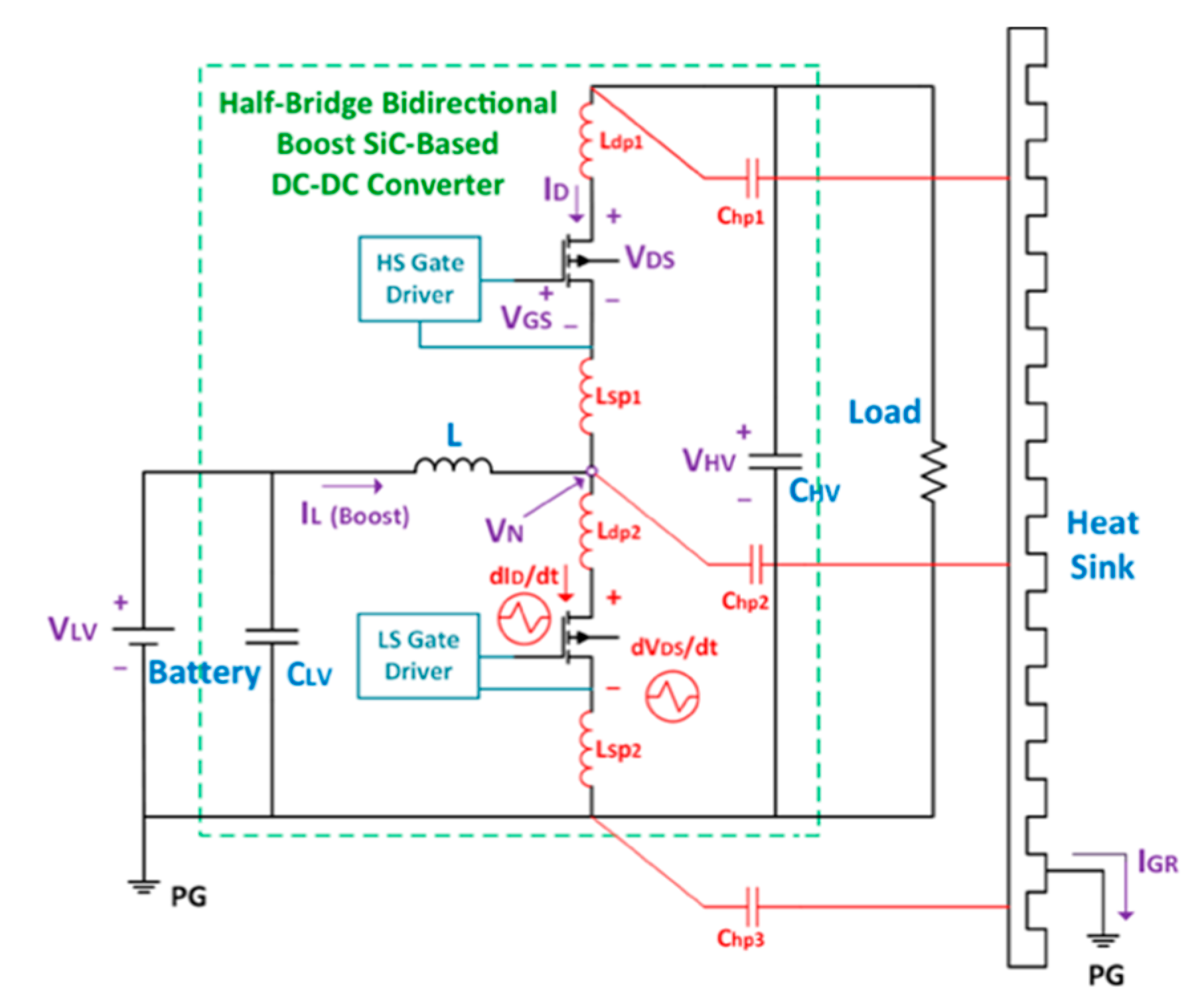
Figure 1. Half-bridge bidirectional boost SiC-based DC-DC converter.
Energies 13 03720 g001
Figure 2. High side (HS) and low side (LS) gate drivers.
Energies 13 03720 g002
Figure 3. HS/LS bipolar power supplies.
Energies 13 03720 g003
Figure 4. Flow chart of the multi-objective optimization design approach.
Energies 13 03720 g004
Figure 5. Test set-up and measurement tools.
Energies 13 03720 g005
Figure 6. 3D PCB board (Altium).
Energies 13 03720 g006
Figure 7. Spectra diagram of the ground current in the conventional gate resistor design.
Energies 13 03720 g007
Figure 8. 3D mesh plot of the regression functions: (a) Efficiency ( η ); (b) EMI Level ( I ^ GR ).
Energies 13 03720 g008
Figure 9. Pareto front of the solved multi-objective optimization problem.
Energies 13 03720 g009
Figure 10. Spectra diagram of the ground current in the optimum gate resistor design.
Energies 13 03720 g010
Figure 11. V DS LS (red color signal with division scale of 20 V) and I GR (yellow color signal with division scale of 500 mA): (a) Optimum design; (b) Conventional design.
Energies 13 03720 g011
Table 1. Power stage specifications of the converter.
ParameterValue
SiC MOSFET [V, A]SCT3022AL (650, 93)
Inductor L [m H ]2.55
Low voltage CLV [ μ F ]50
High voltage CHV [ μ F ]100
Maximum input/output voltage [V]300/600
Switching frequency [kHz]100
Table 2. Gate driver specifications of the converter.
ParameterValue
Gate driver ICSi8271
Input voltage range3.3/5 V
Peak current4 A
OutputSink/Source
Gate Driver Parameters
Ferrite beads (FBHS/FBLS)MPZ1608S221A
220 Ω @ 100 MHz
Zener diodes (DZHS/DZLS)2.4 V
Diodes (DHS/DLS)20 V
Capacitors (CHS/CLS)1 μ F
Bipolar Power Supply
Drive voltage+20/−5 V
Resistors (R1/R2)1 k Ω
Capacitors (C1/C2/C3)4.7 μ F
Zener diode (DZ)20 V
Table 3. Specifications of the measurement tools.
ParameterValue
Input/output Current ProbeAgilent 1146A
Current range100 mA–100 A
Bandwidth100 kHz
Ground Current ProbeAgilent N2893A
Maximum current15 A
Bandwidth100 MHz
Differential Voltage ProbeAgilent N2791A
Bandwidth25 MHz
OscilloscopeDSO-X 3054A
Table 4. Test condition.
ParameterValue
Input voltage [V]25
Duty cycle [%]50
Output power [W]75
Switching frequency [kHz]100
Table 5. Result Comparison for the two design cases.
DesignR-HS-OFFR-LS-ONEfficiencyEMI Level
Conventional2.2 Ohm4.7 Ohm0.9530175.56 μAdB
Optimum1.5 Ohm14 Ohm0.9624172.33 μAdB