Article

Power-Efficient Driver Circuit for Piezo Electric Actuator with Passive Charge Recovery

Toyota Central R&D Labs. Inc., Aichi 480–1192, Japan
*
Author to whom correspondence should be addressed.
Energies 2020, 13(11), 2866; https://doi.org/10.3390/en13112866
Submission received: 13 April 2020 / Revised: 29 May 2020 / Accepted: 2 June 2020 / Published: 4 June 2020
(This article belongs to the Section F: Electrical Engineering)

Abstract

:
Piezoelectric actuation is a promising principle for insect-scaled robots. A major concern while utilizing a piezoelectric actuator is energy loss due to its parasitic capacitance. In this paper, we propose a new concept to recover the charge stored in the parasitic capacitance; it requires only three additional lightweight passive components: two diodes and a resistor. The advantages of our concept are its small additional mass and simple operating procedure compared with existing charge recovery circuits. We provided a guideline for selecting a resistor using a simplified theoretical model and found that half of the charge can be recovered by employing a resistor that has a resistance sufficiently larger than the forward resistance of the additional diode. In addition, we experimentally demonstrated the concept. With a capacitive load (as a replacement for the piezoelectric actuator), it was successfully observed that the proposed concept decreased the power consumption to 58% of that in a circuit without charge recovery. Considering micro aerial vehicle (MAV) applications, we measured the lift-to-power efficiency of a flapping wing piezoelectric actuator by applying the proposed concept. The lift force was not affected by charge recovery; however, the power consumption was reduced. As a result, the efficiency was improved to 30.0%. We expect that the proposed circuit will contribute to the advancement of energy-saving microrobotics.

Graphical Abstract

1. Introduction

Insect-scaled robots have attracted attention owing to their potentially diverse applications: rescue missions, inspections of building structures, and remote sensing. Various types of insect-scaled robot have been created, such as micro aerial vehicles (MAVs) [1,2,3], walking/running robots [4,5,6], and swimming robots [7,8]. One of the most important components of the robot is the actuator; therefore, many actuation mechanisms and principles have been researched. Actuation based on the piezoelectric effect- is considered to be the most promising in terms of power density and output power [9]. For example, an insect-inspired MAV called “RoboBee,” which is developed by a group of Harvard University students, is the lightest and smallest vehicle capable of tethered controlled flight at present [1,2]. They employed a piezoelectric bimorph actuator to flap wings.
Power efficiency is one of the most important performance aspects of flight robots because lower efficiency requires larger mass of an on-board battery. During piezoelectric actuation, energy loss in parasitic capacitance is a crucial concern; it can significantly deteriorate the electrical–mechanical power conversion efficiency of the system. Note that here we define “parasitic capacitance” as the capacitive component of a piezoelectric actuator due to its dielectricity. Figure 1a shows a simplified structure of a flapping wing actuator to explain the loss mechanism. It consists of a piezoelectric bending actuator and a wing. The piezoelectric actuator comprises a laminated layer of a piezoelectric and elastic plate. By applying a voltage to the actuator, a strain is induced in the piezoelectric layer by the piezoelectric effect, and this strain bends the actuator, which in turn causes the wing to flap. By applying an alternating current (AC) voltage with a frequency that matches with the actuator’s resonance, large flapping motion can be produced. Figure 1b shows a simple circuit composed of a DC voltage source and a switch. By switching the connection between the direct current (DC) voltage source and the ground repeatedly, we can apply a square voltage wave to the actuator. The piezoelectric actuator can be equivalently represented by a parallel circuit of a parasitic capacitance C and an impedance Z m ; the circuit expresses the mechanical system in a simplistic form [10]. The electrical power consumed by Z m is identical to the mechanical output power. The focus of this study is on parasitic capacitance. When the switch is connected to the DC voltage source V , energy of ( 1 / 2 ) C V 2 is dissipated through the parasitic resistances, i.e., the switch’s on-resistance. In contrast, when the switch is connected to the ground, the stored energy in C , which is ( 1 / 2 ) C V 2 , is released; therefore, electric power of C V 2 is lost in a cycle. In summary, the stored charge in the parasitic capacitance is fully dissipated using a simple switching driver circuit (a detailed explanation is provided in Section 2). If the charge can be reused, efficiency will be improved. Therefore, many studies have been carried out on charge recovery [11,12,13,14,15,16]. They can be categorized into two methods: one using an inductor and the other with a capacitor. Using the back electromotive force of the inductor, the energy in the parasitic capacitance can be reused to actuate a piezoelectric device [11,12]. Ideally, by employing an inductor with large inductance and low resistance, all the energy in the parasitic capacitance is recovered. The drawback of this method is the inductor’s huge mass, which generally makes the inductor bulky and heavy; therefore, it is not suitable for mobile robot applications.
Several researchers proposed charge recovery circuits that transfer the charge in the parasitic capacitance to another capacitor (or piezoelectric actuator) and reuses it [13,14,15,16]. Their circuits utilizing capacitors are lighter than those with inductors because they are composed of switches. The switching devices must be insulated because the voltage at both ends varies. Such insulated switching devices are still large and heavy, which makes them impractical. There is another approach, which supplies a smoothly varying voltage signal. Karpelson et al. discovered a circuit and control scheme, where a high voltage quasi-sinusoidal wave is output by controlling a DC–DC converter circuit [17]. Theoretically, this is not affected by energy loss due to parasitic capacitance. We concluded that their approach is effective for robots with a few actuators but not suitable for robots with several legs/wings. This is because a robot requires DC–DC converters and feedback controls for each independent actuator.
Therefore, we propose a charge recovery circuit concept, which requires only lightweight passive components. Here, we control a current flow by a resister and diodes but not switching devices. To our knowledge, this is the first report of a passive charge recovery approach. In this study, a guideline for the selection of components based on a simplified theoretical model is provided. In addition, we conduct a demonstration of the proposed concept.

2. Proposed Concept

To clarify the advantages of our new concept, we start by reviewing basic, previously reported driving circuits. Because our concept is based on charge recovery between capacitors, we do not review recovery methods using inductors here. If the energy stored in the parasitic capacitance can be transferred to another capacitor or capacitive component and can be reused, the power efficiency of the system can be improved as stated in the previous section. Campolo et al. created a charge recovery method with two piezoelectric actuators [14]. Edamana et al. also proposed a similar circuit, which included optimal control schemes for precise positioning [15,16]. 
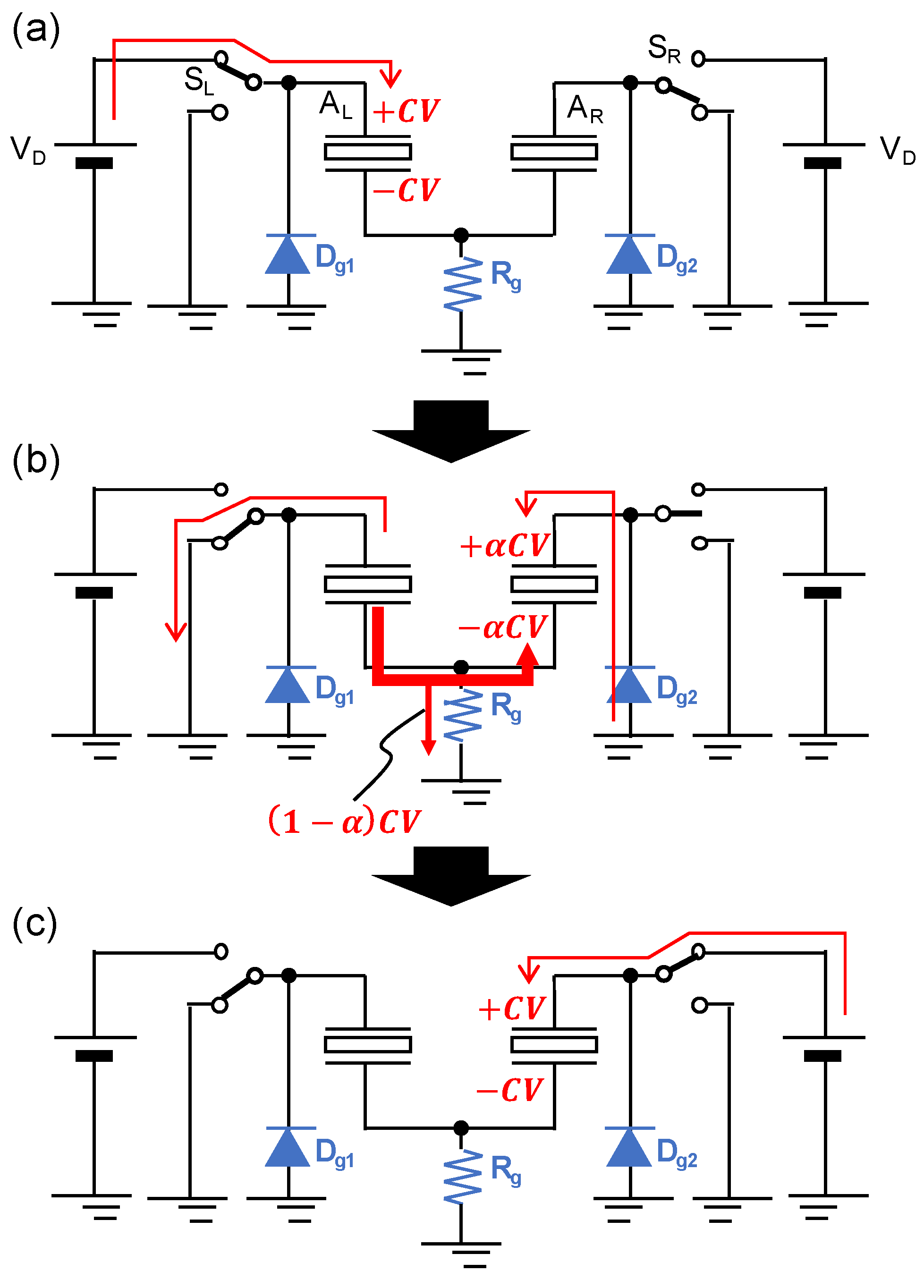
Figure 2 illustrates a simplified circuit of these concepts. Note that the actuator is regarded as a capacitor because we are focusing on the influence of parasitic capacitance. First, the left actuator A L is charged with a charge of C V , which is stored, as shown in Figure 2a. Then, by changing the statuses of both the left and right switches, S L and S R , to open (high impedance), the center switch S C 1 is turned on. Thus, the stored charge moves to the right actuator (Figure 2b).
The ratio of the recovered charge to C V , α depends on the impedance Z c near S C 1 and S C 2 . Campolo et. al. reported that 92% and 75% of the charges were successfully recovered by employing an inductor for Z c with the loads of a capacitor and a bimorph piezoelectric actuator, respectively [14]. Finally, S R is turned to the DC voltage source V D and A R is charged to a potential of V (Figure 2c). A disadvantage of this design is the increase in mass due to the additional switches ( S C 1 and S C 2 ) used for charge recovery. The voltage at both ends of S C 1 and S C 2 varies from ground to V. Common switching devices, such as metal-oxide-semiconductor field-effect transistors (MOSFETs) and bipolar transistors, can not to be used. Due to the high voltage involved, insulated switches like photo-MOS relays are needed. However, such devices are generally much heavier than common transistors. For insect-scaled robots, especially MAVs, their weight is the most important specification since the mass directly determines the required output power. Thus, the weight increase caused by the insulated switches will cancel the efficiency improvement brought about by charge recovery.
Based on previous studies, we sought another approach, which employed only lightweight components and did not use insulated switch devices. Figure 3 shows the concept of the proposed circuit. Similar to Figure 2, we also use a paired piezoelectric circuit and intend to recover the charge between the capacitors. The key components are a resistor in between the actuators, the ground wire R g , and diodes D g 1 and D g 2 , which are connected to the high side of the actuators and colored in blue in the figure. First, A L is charged via S L and a charge of C V is stored (Figure 3a). At this step, A R is set to ground and stores no charge. Next, S L is connected to ground and S R is set to high-impedance status (Figure 3b). If the impedance from A L to A R is smaller than R g , the charge stored in A L flows to A R instead of to the ground. A partial amount of the charge, α C V ,     ( 0 < α < 1 ) will be recovered. The unrecovered energy ( 1 α ) C V is consumed by R g and other resistivity through the current path. D g 2 blocks the charge to be released. Finally, S R is connected to the DC voltage source V D and A R is charged to a potential of V (
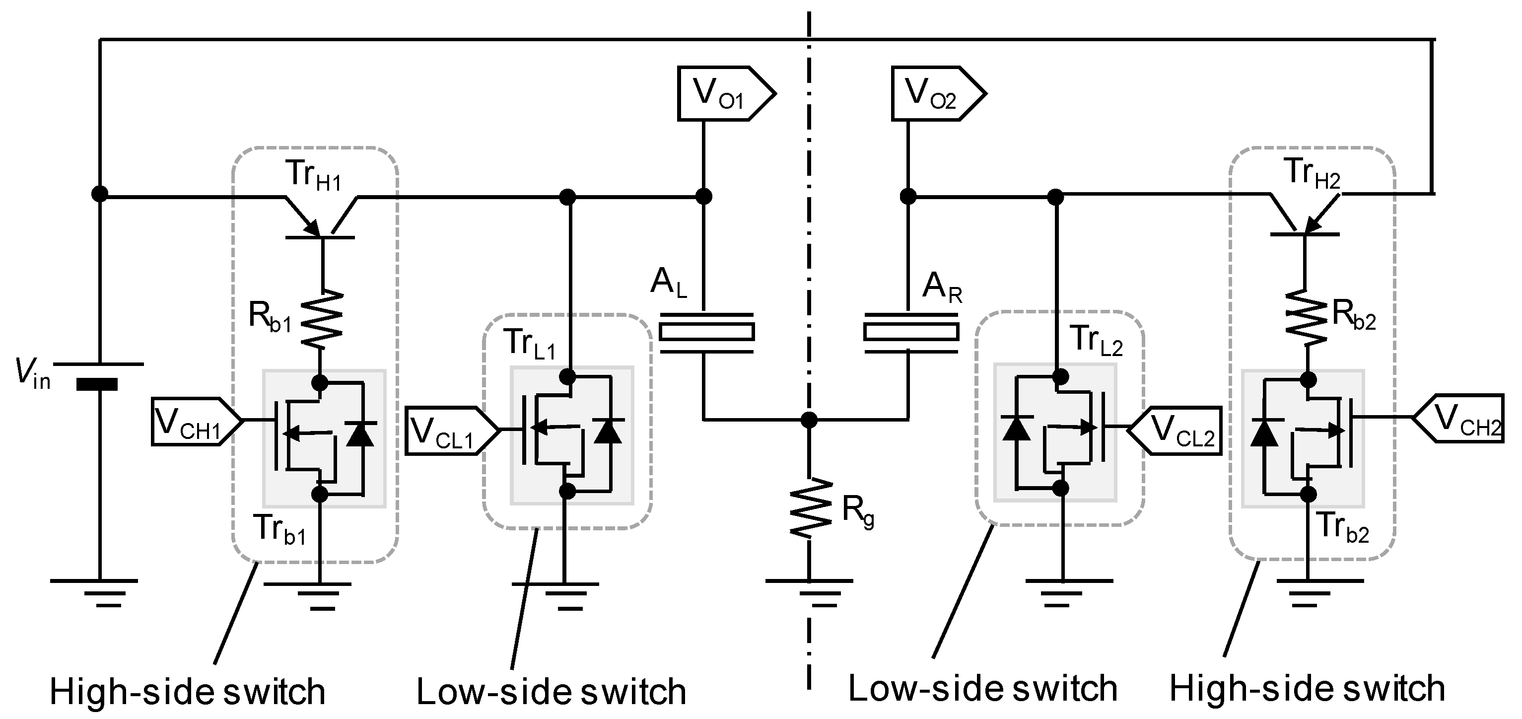
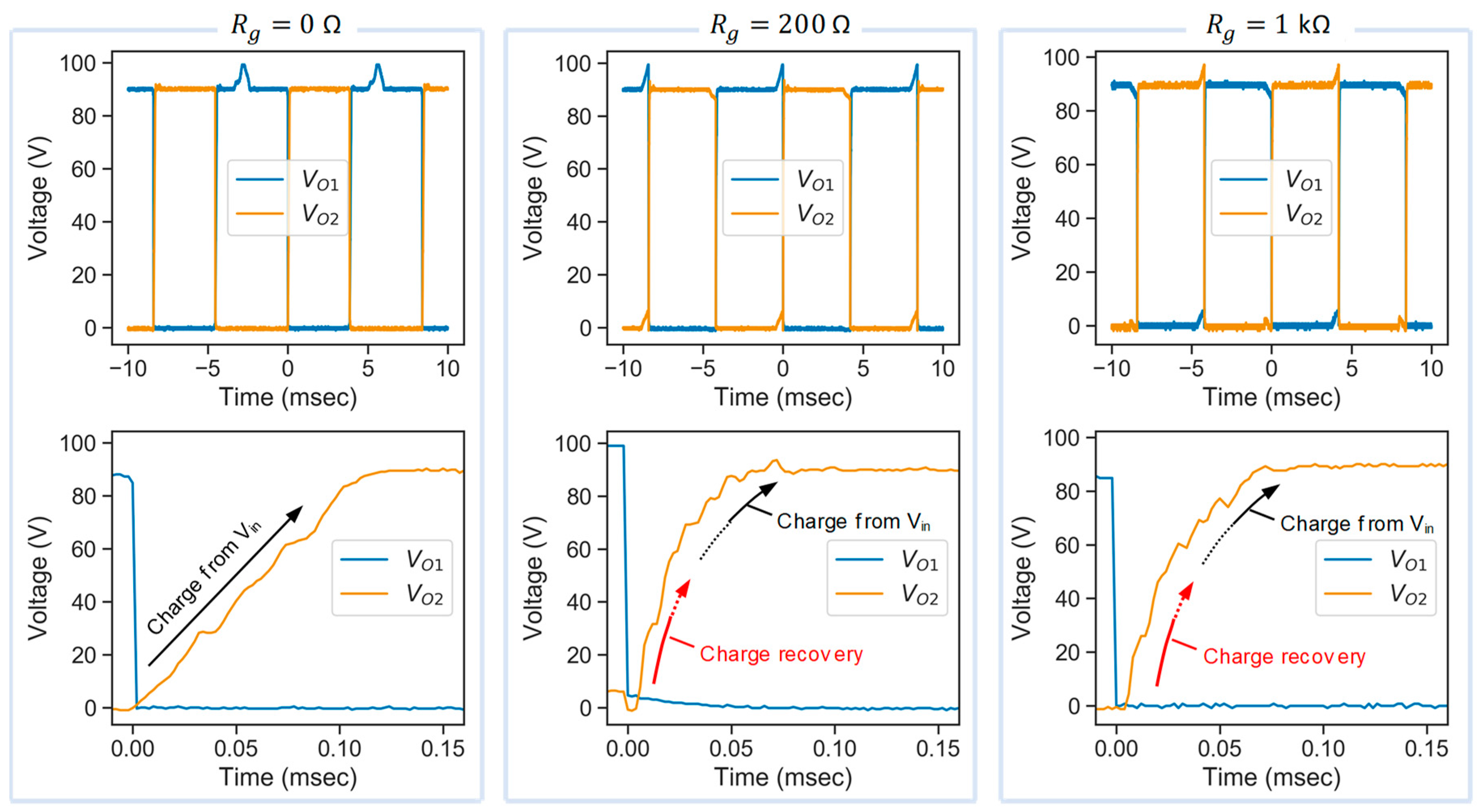
Figure 3c). This approach is realized using only three passive components and their weight increase is smaller than the conventional charge recovery circuits. In addition, utilizing MOSFET for the low-side switches, the two diodes can be omitted because the general commercial MOSFET includes a parasitic body diode. Therefore, this approach can be realized with an additional resistor.
Here, we examined the amount of recovered charge expected from this concept based on a simplified theoretical model. Figure 4 shows the extracted, simplified circuit of the concept. We only consider the charge transition behavior at the switching moment. Before switching, A L and A R have stored a charge of C V in and 0, respectively. When t = 0 , the high side of A L is connected to the ground. The equations express the system and initial conditions are as below:
q 1 C + R g j g = 0 q 2 C + R on q 2 ˙ + R g j g = 0 q 1 ˙ + q 2 ˙ = j g } ,
q 1 ( 0 ) = q 10   ( = C V in ) ,     q 2 ( 0 ) = 0 ,
where C ,     q 1 ,     q 2 , and j g are capacitance of the capacitors ( A L and A R ), the charge stored in A L , charge stored in A R , and the current flowing through R g , respectively. R on represents the forward resistance of the diode D g 2 . Defining a = ( C R on ) 1 and b = ( C R g ) 1 , Equation (1) can be transformed as:
d d t [ q 1 q 2 ] = [ a b a a a ] [ q 1 q 2 ] .
With the initial condition (Equation (2)), this can be solved as:
q 1 ( t ) = q 10 2 d e h t [ b ( 1 e d t ) + d ( 1 + e d t ) ] q 2 ( t ) = q 10 d a   e h t [ 1 e d t ] } ,
where d = 4 a 2 + b 2 and h = ( 2 a + b + d ) / 2 . The diode prohibits q 2 to flow to the ground; q 2 is kept at a local maximum value. This is derived by solving q 2 ˙ = 0
q 2 ˙ ( t ) = q 10 d a   e h t [ h + ( h + d ) e d t ] .
Because ( q 10 / d ) a   e h t > 0 , q 2 ˙ = 0 equal to h + ( h + d ) e d t = 0 . Solving this equation, the time at the local maximum q 2 , t peak is obtained as:
t peak = 1 d ln h h d = C 4 R on 2 + R g 2 ln [ 1 2 ( 2 + R on R g + 4 R g R on + 4 R on 2 + R g 2 ( R on + 2 R g ) ) ] .
As the result of the switching operation, q 2 finally becomes:
q 2 ( t peak ) = q 10 a h d [ h h d ] h d .
Thus, the ratio of the recoverable charge, α , is expressed as:
α = q 2 ( t peak ) q 10 = a h d [ h h d ] h d = 2 R g R on + 2 R g + R on R g 4 R on 2 + R g 2 ( R on + 2 R g + R on R g 4 R on 2 + R g 2 R on 2 R g + R on R g 4 R on 2 + R g 2 ) 1 2 R on + 2 R g 2 R on R g 4 R on 2 R g 2 .
Here, assuming R on R g and defining γ = R g / R on , α and t peak can be approximated as:
t peak C R on 2 ln ( 2 + 5 2 γ ) ,
α 2 γ ( 1 + 4 γ ) 1 1 4 γ ,
Figure 5 shows the relationship between α and t peak ^   ( = t peak / ( C R on ) ) to γ . This graph suggests that a larger γ results in a higher α ; α asymptotically approaches the maximum value of 50%. In addition, it was also found that a larger γ led to an increase in t peak . To obtain both small t peak and large α , we considered 10 1 γ 10 3 as the preferred range. Given that R on is generally around 1 Ω, we employed resistances less than 1 kΩ for
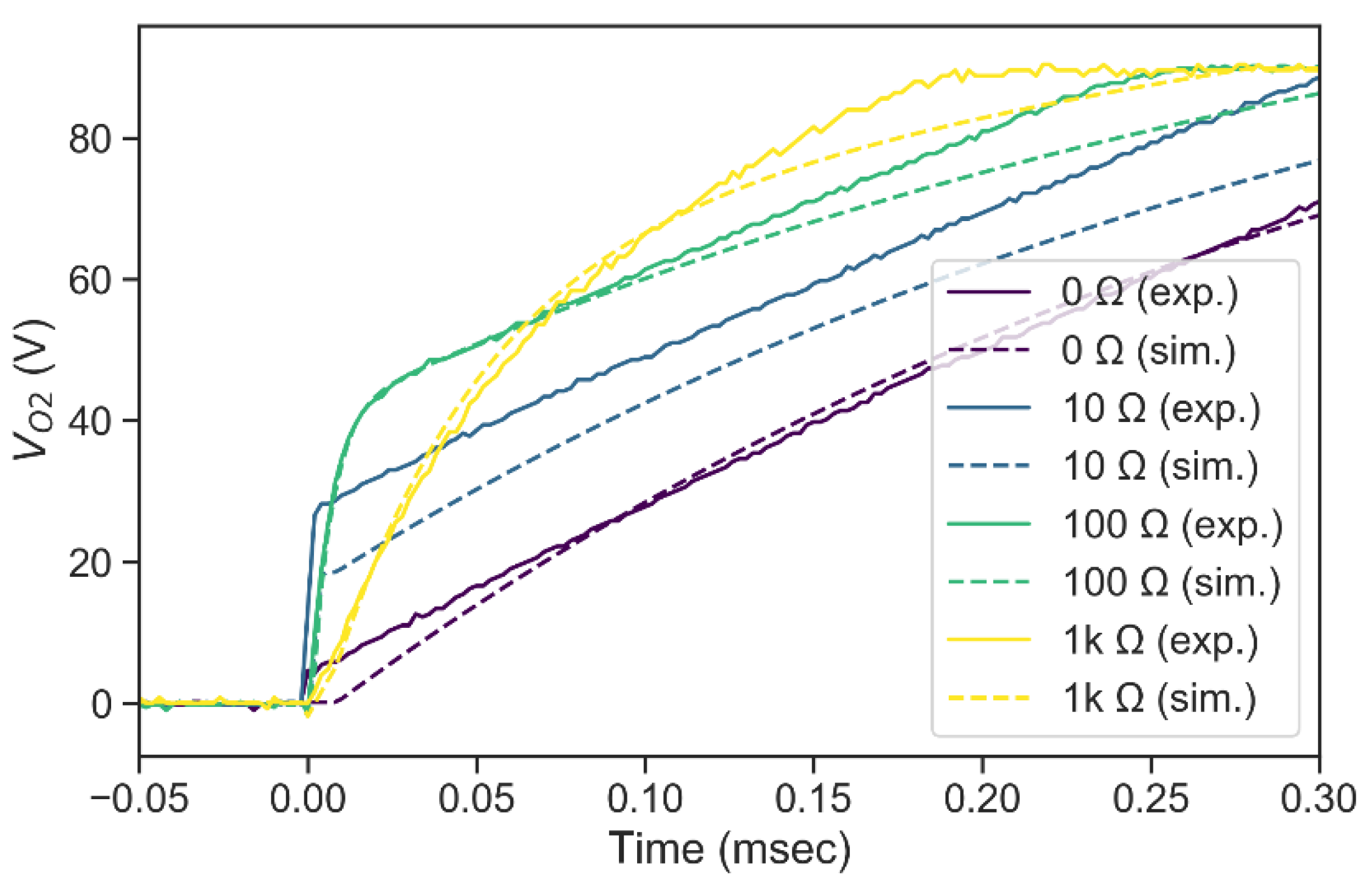
 R g in the experiment.

3. Method

In this study, we fabricated an evaluation circuit and measured its output voltage waveforms and consumed power to validate our concept. We used two types of load: a capacitor and an actual flapping-wing piezoelectric actuator. The charge recovery phenomenon can be more clearly evaluated with the capacitor because it does not contain an electro-mechanical coupling effect. We used the capacitor to valid the basic concept. The actual piezoelectric actuator is used to demonstrate the net efficiency (lift-to-power efficiency).

3.1. Circuit Design

Figure 6 shows the schematic of the fabricated circuit. The high-side switches are composed of bipolar transistors ( Tr H 1 ,   Tr H 2 ), whose bias current is controlled by n-type MOSFETS ( Tr b 1 ,   Tr b 2 ). The low-side switches are realized by n-type MOSFETS ( Tr L 1 ,   Tr L 2 ). When a high-level signal is input to a control port V CH 1 , Tr b 1 changes to close state. Then, a current determined by R b 1 flows through the base of Tr H 1 , and Tr H 1 is turned on (close state). As the result, the high voltage V in is applied to the actuator. When a high-level signal is input to V CL 1 , Tr L 1 shifts to close state. Therefore, the actuator is connected to ground. As stated above, we utilized the body diodes of Tr L 1 and Tr L 2 for D g 1 and D g 2 , respectively. The components used are summarized in Table 1. In this experiment, the high voltage level V in was supplied by a DC voltage source (PMX350-0.2A, Kikusui Electronics Corp.) and we set V in = 90 V in this experiment. Control signals for the switches, V CH 1 ,     V CL 1 ,     V CH 2 , and V CL 2 , were produced using function generators (Wave Factory 1942, NF Corporation). The frequency was configured as 119 Hz, which is the resonant frequency of the flapping wing actuator that was previously measured (see Appendix A).
Next, we explain the control signals; Table 2 summarizes the connection status of the actuator and the signals. When V CHx and V CLx ( x = 1 or 2 ) are set high and low, respectively, the actuator’s electrode is connected to the voltage source. When V CHx and V CLx are set low and high, respectively, the actuator’s electrode is connected to ground. When both V CHx and V CLx are low, the actuator’s electrode changes to the open state (high impedance). Figure 7 shows the control waveform utilized in the experiment. At the start of a period, A L is charged by the DC voltage source ( [ V CH 1 ,   V CL 1 ,   V CH 2 ,   V CL 2 ] = [ High , Low , Low , High ] ), whereby V CH 1 and V CL 2 are flipped to low. As a result, the connection statuses of both actuators become open. We define this moment as t = t 0 Then, V CL 1 and V CH 2 are flipped to high at t = 0.01 T + t 0 where T is the period of the flapping frequency. At this moment, the potential of A L falls to ground, and the charge recovery occurs. At the same time, A R is being charged via the DC voltage source. After t = 0.5 T + t 0 the same procedure is repeated by reversing the left and right signals.

3.2. Measurement

The load capacitor was ceramic with capacitance of 50 nF (GRM55DR73A104KW01L, Murata). Figure 8a is a photograph of the flapping wing driver, whose structure is same as that shown in Figure 1b. This actuator is a trapezoidal-shaped piezoelectric unimorph. We employed Pb(In1/2Nb1/2)O3-Pb(Mg1/3Nb2/3)O3-PbTiO3 (PIN-PMN-PT) as the piezoelectric material owing to its high piezoelectric coefficient ( d 32 = 1156 pm/V [18]). We used titanium for the elastic layer. The thicknesses of the PIN-PMN-PT plate and titanium shim are 100 μm and 130 μm, respectively. This unimorph has a parasitic capacitance of about 25 nF. The wing is composed of a carbon fiber-reinforced plastic leading-edge bar, polyimide/titanium laminated veins, and a polyester film. The wingspan length and chord width are 32 mm and 8.3 mm, respectively.
Figure 8b,c shows the schematic and photograph of the measurement setup, respectively. We measured the voltage waveforms and the consumed power using an oscilloscope (DPO4034B, Tektronix, Beaverton, OR, USA) and a power analyzer (PA1000, Tektronix, Beaverton, OR, USA), respectively. The average lift force was measured with a precision electric balance (HR-100A, A&D Company Limited, Tokyo, Japan). Two actuators were rigidly fixed on a bracket and placed on the electric balance.

4. Results and Discussion

4.1. Capacitive Load

First, we verified results of evaluation using capacitors as load to check whether our charge recovery concept works. Figure 9 shows the voltage waveforms with different R g at V O 1 and V O 2 ; in this experiment, we attached R g of 0 Ω, 10 Ω, 100 Ω, and 1 kΩ, and their characteristics were measured. When R g = 0 Ω, the voltage linearly increased; this is due to regulation by bipolar transistors. In contrast, with R g = 10 Ω and 100 Ω, two-step voltage rising was observed; the first rapid rising is an evidence of charge recovery. A large R g resulted in a smooth voltage transition. This is due to increase in the time-constant of the circuit.
We compared these results through circuit simulation, utilizing HSPICE (Synopsys) in this study. The result is shown in Figure 10. In the case of R g > 100 Ω, the experimental and simulated results are similar. When R g decreased, relatively large discrepancies between the experimental values and the simulated values were observed; for example, the rapidly rising voltage that was simulated with R g = 10 Ω was smaller than the measured one. This seems to be due to inconsistent resistances among the switching devices. Overall, the recorded behaviors were well reproduced by the simulation. This suggests that the fabricated circuit realized the proposed concept.
We also measured the average consumed power with different R g . The measured and Simulation program with integrated circuit emphasis (SPICE) simulation results are summarized in Figure 11. The energy saving effect was clearly observed. When R g = 1 kΩ, the power consumption decreased to 58%, unlike when R g = 0 Ω. This result was well agreed with the SPICE simulation; the simulated power consumption with R g = 1 kΩ was 55% of that with R g = 0 Ω. As described in Section 2, half of the electrical power will ideally be recovered by the concept. We expect that the difference between the ideal and experiment was caused by loss in the switching driver. Although the theoretical consideration does not include any loss in the switches, actual switches do experience some energy loss in operation.

4.2. Piezoelectric Actuator Load

In Figure 12, the measured voltage waveforms at V O 1 and V O 2 are shown. In this experiment, we measured the characteristics with R g being 0 Ω, 200 Ω, and 1 kΩ. Compared to the case with R g = 0 Ω, the voltage rise increased with increase in R g . Although the waveforms were unclear relative to the capacitor, the initial steep region seemed to indicate the charge recovery phenomenon. The ambiguous waveform was due to the piezoelectric effect; mechanical vibration affected the voltage level of the output port of the circuit.
Similar to Figure 10, we also compared the measurement with the SPICE simulation. The result is shown in Figure 13. The mechanical impedance Z m , of the piezoelectric actuator was simply modelled as a series made of an inductor, capacitor, and resistor with L = 1.10 × 10 3 H, C = 1.63 nF, and R = 112 kΩ, respectively [19]. These parameters were derived by monitoring the frequency response characteristic of the actuator (see Appendix A). The difference between R g = 0 Ω and R g 200 Ω was well reproduced by the simulation. The voltage with R g 200 Ω rose faster than that with R g = 0 Ω. This evidence indicated that charge recovery was realized. However, the simulated trend between R g = 200 Ω and 1 kΩ did not match the measurement. Because the LCR-series model did not include higher-order vibration modes, fast vibration and impulsive response were inaccurate. This possibly caused the inconsistency between R g = 200 Ω and 1 kΩ.
Finally, we measured the average consumed power and average output lift force and calculated the lift-to-power efficiency. The lift force was almost constant with the different R g as shown in Figure 14a. This was a reasonable result. The charge recovery phenomenon was faster than the time period of whole square wave in the range of the measured R g ; therefore, the output voltage waveform was not affected. In contrast, the consumed power decreased as R g increased, as shown in Figure 14b. The power used with R g = 1 kΩ was 21.8% smaller than that with R g = 0 Ω. In addition, the trend of the measured power saving matched the simulation’s trend. With respect to efficiency, 30.0% improvement was demonstrated, as shown in Figure 14c. From these results, we concluded that the proposed concept was effective.

5. Conclusions

In this study, we proposed a new charge recovery circuit concept, which required only three lightweight passive components, a resistor, and two diodes. In addition, using general MOSFET for the switching devices, the diodes can be omitted; the proposed concept in practice needs only an additional resistor. We presented a guideline that can be used to select the resistance based on a simplified theoretical model. In addition, we successfully demonstrated that power efficiency improved when the concept was employed in the circuit.
This concept is limited to a paired-actuator system because the charge stored in an actuator should be recovered by another actuator. Since this applies not only to two independent actuators but also a bimorph actuator, which consists of two laminated piezoelectric plates, we consider the possible application field to be wide. Another expected limitation is the switching frequency. The addition of R g makes switching time slower. High-frequency applications, such as ultrasonic transducers, are not suitable for this concept. In contrast, most micro, insect-scaled robots require relatively low frequency. Therefore, our concept will be applicable to them. For example, the flapping frequency of FWMAV is in the range of 10–100 Hz. In addition, we expect this concept is suitable for piezoelectric actuators with small capacitance. Because the time taken to recover the charge is proportional to the capacitance, larger capacitance results in slower charge recovery. This limits the operating frequency of the actuator. In future, we will attempt to develop a robot equipped with this circuit to realize a power-efficient and lightweight robot.

Author Contributions

Conceptualization, T.O. and N.O.; formal analysis, actuator design/evaluation and writing, T.O.; circuit design and evaluation, N.O. All authors have read and agreed to the published version of the manuscript.

Funding

This research received no external funding.

Conflicts of Interest

The authors declare no conflict of interest.

Appendix A. Frequency Response and Parameter Extraction from a Flapping Wing Actuator

The resonant frequency and the equivalent circuit parameters were identified based on frequency responses of the actuator. The resonant frequency was determined by the peak frequency of the average generated lift force. Figure A1a shows the frequency-lift force curve with the applied voltage amplitude of 30 V. In this measurement, we swept the input frequency with 1 Hz steps. From the graph, it was found that the lift force was maximum when the frequency was 119 Hz. The equivalent circuit parameters were extracted from the frequency–power curve. They were derived by fitting a theoretical response to the measured curve. A square wave with amplitude of V , frequency of ω frequency–power response of the circuit model, and a parallel circuit of C p and an LCR-series is expressed based on the Fourier series expansion as follows:
P ( ω ) = C p V 2 ω 2 π + k = 0 P avg ( ( 2 k + 1 ) ω ,   V ) P avg ( ω ,   V ) = 1 2 k + 1 2 π V R ω 2 R 2 ω 2 + L 2 ( ω 2 ( L C ) 1 ) 2 } .
By fitting this function to the experimental data, we obtained L = 1.10 × 10 3 H, C = 1.63 nF, R = 112 kΩ, and C p = 30.8 nF. Figure A1b shows the measured data (blue circle) and fitted curves (orange dotted line).
Figure A1. Frequency response of flapping wing actuator: (a) frequency-lift curve, (b) frequency–power curve with fitted line.
Energies 13 02866 g0a1
In addition, to validate the measured resonant frequency, we calculated the resonant mode shapes and frequencies by finite element analysis (FEA) using COMSOL Multiphysics. Figure A2 shows the result. The first mode indicates flapping motion and its frequency is 119.8 Hz, which is close to the measured frequency. We summarize the material properties used in this analysis in Table A1.
Figure A2. Resonant modes of flapping-wing actuator.
Energies 13 02866 g0a2
Table A1. Material properties used in finite element analysis (FEA) analysis.
MaterialYoung’s Modulus (GPa)Density (kg/m3)
PIN-PMN-PT14.3 *8000
Titanium1004500
Carbon fiber-reinforcing plastic1501500
Polyimide9.01500
Polyester5.01500
* Value was calculated as the reciprocal of the elastic compliance s 22 E .

References

  1. Wood, R.J. Lift off of a 60 mg flapping-wing MAV. In Proceedings of the IEEE/RSJ International Conference on Intelligent Robots and Systems, San Diego, CA, USA, 29 October–2 November 2007; pp. 1889–1894. [Google Scholar]
  2. Ma, K.Y.; Chirarattananon, P.; Fuller, S.B.; Wood, R.J. Controlled flight of a biologically inspired, insect-scale robot. Science 2013, 340, 603–607. [Google Scholar] [CrossRef] [PubMed] [Green Version]
  3. Ozaki, T.; Hamaguchi, K. Bioinspired flapping-wing robot with direct-driven piezoelectric actuation and its takeoff demonstration. IEEE Robot. Autom. Lett. 2018, 3, 4217–4224. [Google Scholar] [CrossRef]
  4. Baisch, A.T.; Wood, R.J. Design and fabrication of the Harvard ambulatory microrobot. In Proceedings of the 14th International Symposium of Robotics Research, Lucerne, Switzerland, 31 August–3 September 2009; pp. 715–730. [Google Scholar]
  5. Hoffman, K.; Wood, R.J. Towards a multi-segment ambulatory microrobot. In Proceedings of the IEEE International Conference on Robotics and Automation, Anchorage, AK, USA, 3–8 May 2010; pp. 1196–1202. [Google Scholar]
  6. Rios, S.; Fleming, A.J.; Yong, Y.K. Monolithic piezoelectric insect with resonance walking. IEEE/ASME Trans. Mechatron. 2018, 23, 524–530. [Google Scholar] [CrossRef]
  7. Erturk, A.; Delporte, G. Underwater thrust and power generation using flexible piezoelectric composites: An experimental investigation toward self-powered swimmer-sensor platform. Smart Mater. Struct. 2011, 20, 125013. [Google Scholar] [CrossRef]
  8. Ming, A.; Hashimoto, K.; Zhao, W.; Shimojo, M. Fundamental analysis for design and control of soft fish robots using piezoelectric fiber composite. In Proceedings of the 2013 IEEE International Conference on Mechatronics and Automation, Takamatsu, Japan, 4–7 August 2013; pp. 219–224. [Google Scholar]
  9. Karpelson, M.; Wei, G.-Y.; Wood, R.J. A review of actuation and power electronics options for flapping-wing robotic insects. In Proceedings of the 2008 IEEE International Conference on Robotics and Automation, Pasadena, CA, USA, 19–23 May 2008; pp. 779–786. [Google Scholar]
  10. Goldfarb, M.; Celanovic, N. Modelling piezoelectric stack actuators for control of micromanipulation. IEEE Control. Systems Mag. 1997, 17, 69–79. [Google Scholar]
  11. Liu, Y.P.; Vasic, D.; Wu, W.J.; Costa, F.; Lee, C.K. Design of fixed-frequency controlled radial-mode stacked disk-type piezoelectric transformers for DC/DC converter application. Smart Mater. Struct. 2009, 18, 085025. [Google Scholar] [CrossRef]
  12. Liu, Y.P.; Vasic, D.; Costa, F. Wideband ZVS half-bridge circuit for piezoelectric transformers with small inductance. Electron. Lett. 2012, 48, 523–524. [Google Scholar] [CrossRef]
  13. Main, J.A.; Newton, D.V.; Massengill, L.; Garcia, E. Efficient power amplifiers for piezoelectric applications Smart Mater. Struct. 1996, 5, 766. [Google Scholar]
  14. Campolo, D.; Sitti, M.; Fearing, R.S. Efficient charge recovery method for driving piezoelectric actuators with quasi-square waves. IEEE Trans. Ultrason. Ferroelectr. Freq. Control. 2003, 50, 1–10. [Google Scholar] [CrossRef] [PubMed] [Green Version]
  15. Edamana, B.; Oldham, K. Optimal on-off controller with charge recovery for thin-film piezoelectric actuators for an autonomous mobile micro-robot. In Proceedings of the American Control Conference, San Francisco, CA, USA, 29 June–1 July 2011; pp. 3465–3470. [Google Scholar]
  16. Edamana, B.; Oldham, K. Optimal low-power piezoelectric actuator control with charge recovery for a microrobotic leg. IEEE/ASME Trans. Mechatron. 2013, 18, 251–262. [Google Scholar] [CrossRef]
  17. Karpelson, M.; Wei, F.Y.; Wood, R.J. Driving high voltage piezoelectric actuators in microrobotic applications. Sens. Actuators Phys. 2012, 176, 78–89. [Google Scholar] [CrossRef]
  18. Sun, E.; Zhang, S.; Luo, J.; Shrout, T.R.; Cao, W. Elastic, dielectric, and piezoelectric constants of Pb(In1/2Nb1/2)O3-Pb(Mg1/3Nb2/3)O3-PbTiO3 single crystal poled along. Appl. Phys. Lett. 2010, 97, 032902. [Google Scholar] [CrossRef] [PubMed] [Green Version]
  19. Katz, H.W. Solid State Magnetic and Dielectric Devices; John Wiley Sons, Inc.: London, UK, 1959. [Google Scholar]
Figure 1. Piezoelectric flapping-wing actuator and its basic driver circuit: (a) principle of piezoelectric actuation; (b) a driver circuit with simple switch.
Energies 13 02866 g001
Figure 2. Conventional charge recovery circuit: (a) left actuator is charged by the direct current (DC) source; (b) charge is transferred to the right actuator through the charge recovery circuit; (c) right actuator is charged by the DC source.
Energies 13 02866 g002
Figure 3. Proposed charge recovery circuit: (a) the left actuator is charged by the DC source; (b) when the left actuator is switched to ground (GND), a portion of the charge is transferred to the right actuator; (c) the right actuator is charged by the DC source.
Energies 13 02866 g003
Figure 4. Extracted circuit to derive theoretical model.
Energies 13 02866 g004
Figure 5. (a,b) Relationship between γ , α , and t peak ^ .
Energies 13 02866 g005
Figure 6. Design of fabricated circuit.
Energies 13 02866 g006
Figure 7. Waveform of control signals (not to scale).
Energies 13 02866 g007
Figure 8. Samples and setup: (a) flapping-wing actuator; (b) schematic and (c) photograph of measurement setup.
Energies 13 02866 g008
Figure 9. Voltage waveform with load of capacitors with different R g .
Energies 13 02866 g009
Figure 10. Comparison of experimental and SPICE simulated voltage waveform with load of capacitors.
Energies 13 02866 g010
Figure 11. Power consumption with different R g .
Energies 13 02866 g011
Figure 12. Voltage waveform with load of flapping wing piezoelectric actuator with different R g .
Energies 13 02866 g012
Figure 13. Comparison of experimental and SPICE simulated voltage waveform with load of a flapping wing piezoelectric actuator.
Energies 13 02866 g013
Figure 14. Performance of proposed circuit: (a) lift force, (b) power consumption, and (c) lift-to-power efficiency.
Energies 13 02866 g014
Table 1. Electrical component list.
Part SymbolPart NumberManufacturer
Tr H 1 ,   Tr H 2 PMSTA92Nexperia
Tr b 1 , Tr b 2 SiB452DKVishay
Tr L 1 ,   Tr L 2 SiB452DKVishay
R b 1 ,   R b 2 RK73H1ETTP1R00FKOA
Table 2. Relationship between actuator’s connection status and control signals.
Connection Status V C H x * V C L x *
V in HighLow
GNDLowHigh
Open (high impedance)LowLow
* x = 1 or 2.

