Abstract
Voltage profile is one of many aspects that affect power quality in low-voltage distribution feeders. Weak grids have a typically high line impedance which results in remarkable voltage drops. Distribution grids generally have a high R/X ratio, which makes voltage regulation with reactive power compensation less effective than in high-voltage grids. Moreover, these networks are more susceptible to unbalance and harmonic voltage disturbances. This paper proposes an enhanced coordinated control of active and reactive power injected in a distribution grid for voltage regulation. Voltage drop mitigation was evaluated with power injection based on local features, such loads and disturbances of each connection. In order to ensure disturbances rejection like harmonic components in the grid voltages, a repetitive vector-control scheme was used. The injection of coordinated active and reactive power with the proposed control algorithm was verified through simulations and experiments, demonstrating that it is a promising alternative for voltage regulation in weak and low-voltage networks subject to inherent harmonic distortion.
1. Introduction
Low-voltage (LV) distribution systems may suffer from the reduction of voltage amplitude, especially at points far away from the supply locations [1]. A significant voltage drop occurs when both the feeder and line impedance have high values and the drop voltages on these elements assume a considerable value in relation to the voltage delivered to the consumers. In such cases, the grid is called a weak grid [2]. Any branch of a low voltage weak grid may suffer from this effect. Other factors may also influence the quality of the power supplied, such as the voltage distortion at the point of common connection (PCC) produced by non-linear loads that drain currents with a high harmonic content [3]. In weak grids, harmonic distortions become more apparent compared to the fundamental component. This occurs primarily because line impedance is directly proportional to the frequency and the nonlinear current flowing through the branch produces non-fundamental frequency voltage drops.
To address the voltage drop issue, reactive power injection is used to regulate the voltage at specific points located on the grid with traditional reactive control and distribution static synchronous compensators (DSTATCOM). However, this method presents one major drawback: reactive power control is not as effective as in high-voltage grids in consequence of the R/X ratio being usually high in LV grids [4]. On the other hand, several related approaches were introduced in [5,6,7,8] which confirm the effectiveness of active-based voltage regulation. Battery energy storage systems are the most commonly used equipment for storing energy [9,10,11,12]. However, deep discharges, high drain current and high operating temperatures are some issues that reduce the lifespan of those systems [13].
In recent works [4,8,14,15,16], the reactive power control was redesigned to work with active power. Generally, DSTATCOMs use only fundamental–frequency current injection for rms voltage regulation [16,17]. However, the grid voltages and their harmonic distortions are disturbances to the current control. Even if the DSTATCOM reference currents are perfectly sinusoidal and balanced, the grid voltages may affect the controllers’ performance, leading to steady–state errors, distorted injected currents and even instability if not properly addressed during the control design. Furthermore, additional functions can be included in the DSTATCOM control, like compensating load unbalance and harmonic currents. In this case, the controller reference current must have high gain for fundamental frequency positive- and negative-sequence components and for all harmonic components that are expected in the load currents. In order to comply with these requirements, PI conventional controllers with very high bandwidth would be necessary and multiple-frequency controllers based on proportional-resonant actions have been thoroughly investigated, where the latter solution have shown to be preferable. In this sense, repetitive controllers also appear as good candidates as presented in [18,19,20,21,22,23,24,25].
In general, the traditional repetitive control (RC) techniques have a slow dynamic response and a transient performance that is not suitable for controlling the instantaneous variables of pulse-width modulated (PWM) converters. As a result, these RCs are used as plug-in controllers and work in addition to classical controllers, usually proportional-integral (PI) or proportional-resonant (PR) type [18,19,20]. In other cases, repetitive controllers are used for steady state error elimination, where a fast dynamic performance is not necessary. However, complex repetitive vector-control schemes recently proposed have demonstrated better stability and performance characteristics, in comparison with scalar repetitive controllers [26,27]. The use of complex structures of repetitive controllers may be suitable for applications where the controller performance is required in a family of harmonic components [27].
In [21] a conventional RC is used as a plug-in controller capable of regulating all integer harmonic components of a reference signal. This means that, if the reference signal waveform is composed of the fundamental-frequency () component together with any set of integer harmonic components, then the controller ensures zero steady-state error. Furthermore, if the system is subjected to integer harmonic disturbances, the controller rejects them in steady-state. For implementing this controller, all N samples of the signal error in the last fundamental period are necessary (, where is the sampling frequency). In [22,23] a RC designed for regulating odd harmonic components is used since even harmonic components are rarely found in electrical systems. Such selectivity allows the controller to use fewer samples of the signal error and also ensure a faster dynamic response, at the expense of not a ensuring zero steady-state error for even harmonic components. The mentioned idea was extended to allow the design of RCs for controlling a specific group of harmonic components, like , [24], or , where n and m are fixed natural parameters and [25]. For bigger values of parameter n, less harmonic components are regulated, but faster dynamic responses are expected. The RCs described so far can be classified as scalar repetitive controllers. When applied to three-phase systems, one controller should be used to regulate each phase component or, alternatively, after a Clarke coordinate transformation, two of these control structures can be used in the and components [28].
In this paper, we propose a voltage regulation scheme with enhanced disturbance rejection for LV grids using repetitive vector control. The coordinated control of active and reactive power ensures effectiveness in weak grids, while space-vector repetitive controller (SV-RC) design rejects disturbances caused by current distortion and harmonic voltages on point of common coupling. A space-vector controller has a unique structure that facilitates the control design, allows regulating a positive-sequence harmonic component without having to control the negative-sequence component of the same order and improves dynamic performance. Furthermore, our proposed active and reactive power coordinated control determines current references for power injection based on grid structure regarding the R/X ratio. As a result, the lifespan and autonomy of energy storage systems can be improved. It is worth mentioning that such N control technique can be adapted and then employed to any energy storage system, especially in remote electric-vehicle (EV) charging stations, in order to provide voltage regulation as an ancillary service [29]. Thus, depending on the state-of-charge of the batteries connected, it is possible to provide an effective voltage regulation capability with a minimum utilization of the stored energy of the EVs or any other storage system.
The paper is organized as follows: Section 2 presents the control and disturbance model, the SV-RC design focused on fundamental component control and disturbance rejection. Section 3 describes the active and reactive coordinate control as well as the effective voltage and power reading method. Section 4 presents the experimental results demonstrated by a prototype built in the laboratory. Finally, conclusions are presented in Section 5.
2. General Approach
The voltage regulation scheme determines, from the predefined voltage values, the currents to be injected by DSTATCOM. These references are determined based on the power management algorithm described in this section. The repetitive vector-control is used to ensure an effective control of currents, rejecting disturbances caused by imbalances and harmonic voltages on PCC. The proposed voltage regulation system with SV-RC is shown in Figure 1 where linear and non-linear loads, power grid and inverter are all connected to the PCC. An independent power source, a generic energy storage system (ESS), provides dc-link voltage regulation and the required power for the converter operation.
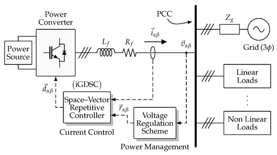
Figure 1.
Voltage regulation system with SV-RC controller.
The converter output current has two input variables: converter duty cycle and the voltage at the PCC , which is considered a disturbance to the control model, as shown in Figure 2. The model equation can be obtained through Clarke coordinate transformation , as shown in (1):
where E is the dc-link voltage, and and are inductance and resistance of output filter, respectively. The two control model inputs, reference signal and disturbance, can be independently treated in a linear time-invariant (LTI) system. The final signal is the sum of individual responses, as shown bellow:
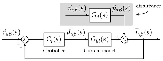
Figure 2.
Simplified disturbance model for current control loop.
Therefore, in order to ensure reference signal tracking and disturbance rejection, condition (3) must be satisfied for all frequencies present in both the reference signal, which is generally a fundamental-frequency positive sequence signal and the disturbance, which is the grid voltage, containing typical harmonic components of positive and negative sequences:
Then, any disturbance will be rejected and the reference signal will be reproduced at the output:
For a system subject to disturbances of different frequencies, such as in the case of voltage regulation when non-linear loads are connected to the PCC, disturbance rejection is an important design requirement.
The voltage and current of the electric network and the currents of the linear and nonlinear loads fed by a weak network are shown in Figure 3. The distorted current absorbed by the nonlinear load distorts the PCC voltage and affects even the currents of the connected linear loads.
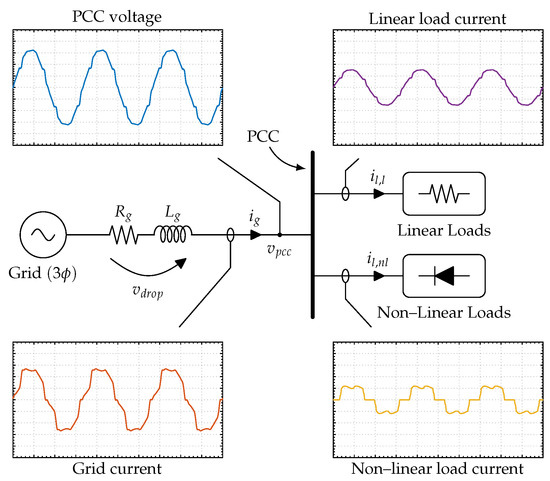
Figure 3.
Effects of linear and non-linear loads fed by a weak grid.
2.1. Current Control Strategy
According to the internal model principle (IMP) the controller can reject disturbances or track references if it incorporates the disturbance model or the reference signal in its transfer function [30]. Thus, multiple resonant poles are required to guarantee null error at steady state if the reference or disturbance signal is distorted, i.e., have multiple harmonic frequencies.
In this sense, we used the SV-RC based on the inverse transfer function of the generalized delayed signal cancellation (iGDSC) [27] to control the converters’ output current. Thus, a proper disturbance rejection capability can be added to the adopted voltage regulation scheme. Such SV-RC has poles located at multiple frequencies in the complex-plane and produces the desired performance with multiple harmonic components. The iGDSC SV-RC transfer function is shown in (6):
where the terms depend on the family of desired harmonic components. The coefficient N is the ratio of the sampling frequency to the fundamental frequency . The operator is a complex number and changes the controller amplitude and phase, however in this application the operator is chosen to maintain the unit gain without additional displacement to the controller, which leads to a real term.
The controller transfer function has the space-vector error signal as input and the space-vector control action signal as output, as shown in (7). Therefore, the final control action signal is obtained in (8) through the discrete transfer function.
The SV-RC controller block diagram is shown in Figure 4. This structure has a positive feedback with a delay block , which produces periodic signal generator, multiplied by a complex value in series with the delay block. The output signal is the sum of the positive feedback signal with the error signal multiplied by a complex value .
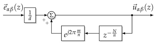
Figure 4.
Block diagram of iGDSC based SV-RC with positive feedback structure.
As described in [27], the Nyquist diagram of the plant to be controlled must be inside the so called stability domain of the repetitive control scheme. Since the origin of the complex plane is not included in the stability domain of the iGDSC SV–RC, it is not possible to obtain adequate performance indexes to control the plant with the design. To increase the controller’s stability domain, i.e., to enhance the system stability, a low-pass filter with unit gain in low frequencies and high attenuation rate in the high frequencies is used. The discrete implementation allows the use of an unconditionally stable digital finite impulse response (FIR) filter with linear phase delay when used with symmetric coefficients [31], as shown in :
where coefficients are symmetric and M is an even number representing the FIR filter order.
The FIR filter can be represented by a constant magnitude part and a linear phase displacement part:
Hence, the filter phase shift is known and can be cancelled by reducing the controller delay samples since this delay also produces a linear phase delay. Let be the original delay and the compensated delay:
The final transfer function is a result of the FIR filter and the linear phase compensation, as shown in (12):
In the digital implementation the computational delay is the time required by the processor to compute a new value from an input sample. This means that there is a delay with the modulation period in the control algorithm. This unit delay produces a response with a smaller phase margin and consequently the step response tends to be underdamped [32]. Therefore, the system may become unstable depending on the control design parameters.
A phase lead compensator is used to attenuate the undesired effect of computational delay. The compensator has the transfer function defined by
where is the compensator gain, is the zero position, is the pole position, is the maximum lead frequency. The term defines the distance between the compensator pole and zero. The condition must be satisfied to maintain the phase lead characteristic:
where is the maximum forward angle, with the following condition: and due to pole position physical limitation [33].
2.2. Design of the Current Controller
This loop must have fast dynamic response and high gain to allow proper reference tracking capability. In Figure 5, all the elements of the internal current control loop are shown: controller designed based on the iGDSC operation, RC gain , phase lead compensator , computational delay with the digital modulator DPWM, represented by , transfer function of the converter filter output current and current sensor .
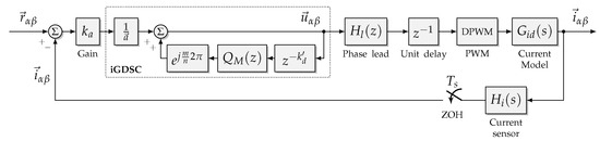
Figure 5.
Block diagram of iGDSC based SV-RC with positive feedback structure.
In Figure 6 Bode (a) and Nyquist (b) diagrams of the output current model and controller open-loop transfer function are shown. The final open-loop transfer function resulted in a zero crossing frequency of , with of phase margin (PM) and of gain margin (GM). The Nyquist diagram is used to check the sensitivity function index value , which provides additional information about the controller stability, especially when exists multiple resonance peaks and multiple 0 dB crossings [34]. The sensitivity function is defined as the inverse of the distance between the Nyquist path and the critical point . The peak sensitivity is the maximum value of the sensitivity function, so higher values indicate the proximity to system instability [35].
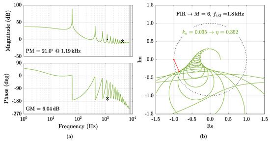
Figure 6.
Nyquist and Bode diagram of final transfer function: (a) Bode diagram; (b) Nyquist diagram.
The cut-off frequency of the FIR filter of order was set to kHz which represents attenuation from the 30th harmonic component. The phase lead compensator was designed with maximum phase advance of at the frequency of to compensate the effects of computational delay, which results and . Moreover, the proportional gain needed to obtain the performance parameters previously presented was .
2.3. Effective Voltage Design Control
This loop controls PCC voltage as a function of the converter current. This control is done by an outer control loop with a slower dynamic than the inner current loop. The difference between loop dynamics has the purpose of decoupling outer and inner control loops and allowing their independent designs. The PCC voltage model is obtained from the equivalent circuit shown in Figure 7. In this model, the converter current is the controlled variable and the other variables are considered disturbances for the voltage control loop.
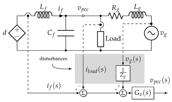
Figure 7.
PCC voltage equivalent model with disturbances.
Therefore, considering load current and grid voltage disturbances for and :
A proportional-integral (PI) controller with additional pole is used for outer loop control. This controller is suitable for constant signals since the integral action has null regime error for this input type. The extra pole is positioned at high frequency to attenuate the effects of higher order harmonic components. The transfer function is shown in (17):
where, is the controller gain, is the zero position and is the pole position, both in .
The control design in the w-plane uses zero-order hold (ZOH) and Tustin discretization methods that allow a frequency response design with well known techniques of the s-plane, taking into account the effects of discretization [36].
The controller is designed with a cross-over frequency of 6 Hz and phase margin of 63. The outer loop sampling frequency is adjusted to be ten times less than the inner loop. Thus the coefficients of the discrete transfer function preserve the precision required for the digital implementation.
3. Coordinated Power Control
As stated earlier, the use of reactive power alone to compensate voltage drop issues for weak LV grids is not as effective as it would be if it was applied to high-voltage systems. On the other hand, the active-power-based voltage regulation provides an improved performance, mainly for grids with high R/X ratio. However, such a technique would demand large energy storage devices if long intervals of operation were required. In this sense, the use of a coordinated control method of active and reactive power for voltage regulation is preferable especially when minimum use of the stored energy is required. Therefore, such feature allows the optimization of the ancillary service minimizing active power injection and, consequently, increasing the batteries’ lifespan.
The active and reactive power coordinated strategy adopted in this paper was proposed by [15] and is performed by some logical operations, which are implemented along with the outer control loop as shown in Figure 8. In such scheme, the in-phase () and quadrature () components of the converter’s reference current are provided in order to maintain the PCC voltage according to its desired range, controlling the amount of active power injected to the minimum required. Therefore, only severe voltage drops would demand active power injection to be compensated.
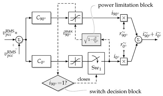
Figure 8.
Logic algorithm used within outer control loop for voltage control.
In order to avoid overlapping of both and control actions, the switch remains opened when the current is lower than the converter rated output current, that is (in pu). If such current component reaches the converted rated current without being able to restore the PCC voltage at its desired range, the switch is turned on. Thus, a small amount of the in-phase current component starts to be provided by the converter in order to enhance the voltage regulation. To hold the apparent power within the converter limits, the power limitation block imposes a dynamic saturation value for the quadrature current , which is equal to (in pu). Once the desired voltage level is achieved, the amount of and are maintained until any other voltage deviation occur.
3.1. Effective Voltage Computation Method
Aiming to guarantee a suitable operation, a precise acquisition of the grid voltage rms value is required. In [15] the authors use the measured rms voltage of only one phase of the system to control the voltage level of all three phases. Then, if the grid voltages are deeply unbalanced, such adoption may lead to inaccurate results and even to severe overvoltage condition to the other two phases that are not considered. In this regard, we have used the effective voltage as a measure of the grid rms voltage which is appropriate for three-phase systems since it aims to take into account the rms voltage levels of the three phases simultaneously.
The phase-to-phase effective voltage for a three-wire system is defined as [37]:
The phase-to-phase voltages are used to obtain the Clarke’s transformation components :
The phase-to-phase effective voltage is calculated using and from (19):
However, the network voltages may have several harmonic components that can lead to distorted values of effective voltage and this distortion becomes relevant in weak grids. For that reason we have adopted the generalized delayed signal cancellation (GDSC) method to detect the fundamental frequency positive sequence (FFPS) of voltage signal [38].
This transformation consists of a complex mathematical operation on a space vector. Current and delayed samples of the input space vector are used to cancel a particular harmonic component family. The GDSC operation is described as
where the terms of the set and define the harmonic component family, n defines the repetition period, m defines the initial frequency component, is the complex operator that defines the operation gain, is the input space vector and is the output space vector.
It is not possible to eliminate all the harmonic components to obtain the FFPS signal vector with only one GDSC transformation, so five cascaded operations are designed to eliminate most of the harmonic components. Each operation eliminates a certain family of harmonic components and when cascaded allows the extraction of FFPS [38].
The first designed transformation eliminates the family, the second transformation eliminates the family, the third transformation eliminates the family, the fourth transformation eliminates the family, the fifth transformation eliminates the family , leaving only the components of the set .
In Figure 9 the filter frequency response magnitude graph is shown. In this graphic, the FFPS has unitary amplitude, i.e., the filter allows FFPS to pass and eliminates or attenuates almost completely the other components. Such components that still persist in the bandwidth are of high order and are practically nonexistent in the measurement system and do not interfere with the final response.
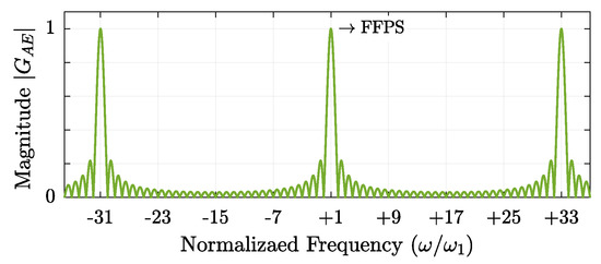
Figure 9.
Magnitude graph of operation FFPS-GDSC as a function of normalized frequency.
Therefore, the effective voltage is then called as effective positive-sequence voltage after the FFPS-GDSC filter operation:
where, and are the resulting voltage components from transformation after FFPS-GDSC operation.
3.2. Active and Reactive Power Reading Method
The power calculation uses the voltage and current components in coordinates. This information is used to check the operating point and the voltage regulation strategy, then it is not used for control or reference generation.
The voltage components filtered by the FFPS-GDSC operation are used to calculate the active and reactive power in three-phase systems:
The abc- blocks of coordinate transformations are shown in Figure 10, they are: the FFPS-GDSC filter block, power and effective voltage calculation.
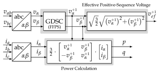
Figure 10.
Method for computing the effective voltage and the active and reactive power calculation.
4. Experimental Results and Discussions
A three-phase three-wire kVA prototype was built in order to demonstrate the operation of the proposed control algorithm, as shown in Figure 11. The converter was connected to a 127 V/60 Hz grid in series with a impedance () formed by a resistor and a inductor, that results in 2.16 of R/X impedance ratio, which is compatible with a weak distribution grid. The converter consists of a three-phase voltage source inverter (VSI) with a switching frequency of 18 , with a second order output filter with inductance and capacitance for switching frequency ripple attenuation. The DC-link of 6600 capacitance operates with 500 of DC voltage. The power modules are mounted on a forced-ventilation aluminum heater and drivers with isolated control signals.
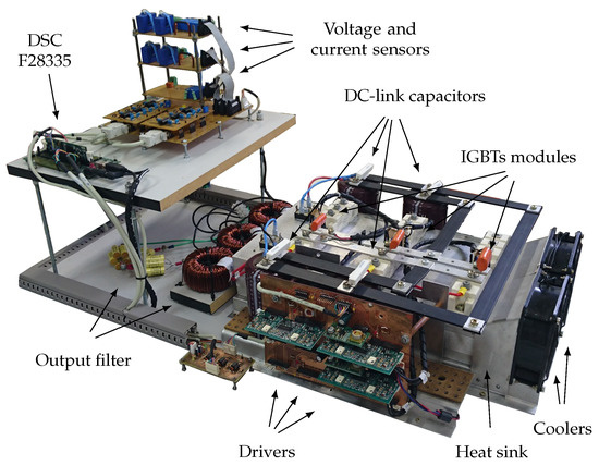
Figure 11.
Three-phase prototype built in laboratory.
It is worth to mention that the currents and voltages measuring tips were attached in the points stated in Figure 7 for all experimental tests that were developed. Thus the converter currents (, and ) were measured in the output filter inductors of each phase and the voltage is the phase-to-phase voltage of the converter output filter capacitor. Such quantities measurements were acquired in the high resolution acquisition mode of the oscilloscope and no internal filter was used.
The setup for experimental results is shown in Figure 12. Converter currents and PCC phase-to-phase voltage in steady state operation are shown in Figure 13a. For comparison purposes, the voltage before the regulation is shown in R2 (black) and after the regulation is shown in CH4 (green). In this test, linear resistive loads of 56 and a three-phase Graetz bridge rectifier are used as linear and nonlinear loads, with commutation inductor of 560 and resistive dc load of as shown in Figure 12a.
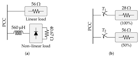
Figure 12.
Setup for experimental results: (a) Steady state results with non-linear loads; (b) Linear load step variation.
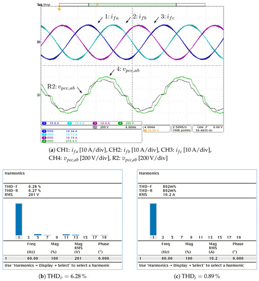
Figure 13.
Experimental results in steady state: (a) Converter currents with low harmonic distortion even with grid distorted voltage; (b) Harmonic voltage analysis; (c) Harmonic current analysis.
The voltage harmonic distortion is the result of a nonlinear load connected in a weak network. It is possible to observe the increase of effective voltage value to nominal value of 220 V with a current of 10 A in each phase with both active and reactive power compensation. Voltage and current total harmonic distortion (THD) are shown in Figure 13b,c. Voltage THD is % and current THD is %, which shows that the controller can reject the disturbances from the high order harmonic components and ensures a pure sinusoidal current.
Steady state waveforms for linear loads are shown in Figure 14a. The currents injected by the converter are composed of pu quadrature and pu in-phase components resulting in 10 A to regulate the PCC effective phase-to-phase voltage at its nominal value of 220 V. Transient results are shown in Figure 14b at the moment the converter starts its operation with the 28 load. It is possible to check the voltage regulation from 193 V to 220 V, while the currents and are changed by the control algorithm. The quadrature reference current reaches its maximum value of 1 pu and from that moment on, the in-phase reference current is activated to reach the desired voltage regulation. Reduction of the quadrature reference current to pu is necessary to keep the converter within the maximum power specification. Finally, the active and reactive power graphs shows power injection of 3450 VAr and 800 W.
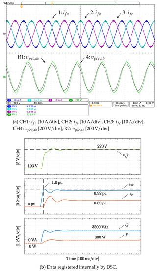
Figure 14.
Experimental results: (a) Converter currents for voltage regulation with linear loads; (b) Results for transient regime: effective voltage, in-phase and quadrature current references and converter injected power.
The results for load step variation are shown in Figure 15a In this test, two loads are selected: 100% (28 ) and 50% (56 ) of nominal load as shown in Figure 12b Initially, the 50% load is connected, being replaced by 100% load. In first test, the 50% load requires only reactive power of 2700 VAr for voltage regulation, however the active power injection (800 W) becomes necessary when the load increases to the nominal values, which can be seen in Figure 15b. The operation duality of the technique works in similar manner, thus, the load variation occurs in the reverse direction, i.e., the load is reduced. As expected, the control returns to the reactive power-only injection condition, which correspond to pu of quadrature reference.
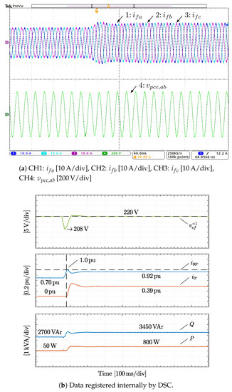
Figure 15.
Experimental results for load change: (a) Converter currents and PCC voltage for load increase; (b) Waveform of positive sequence effective voltage, quadrature and phase current references, and converter injected power to load increase.
5. Conclusions
In this paper, we proposed a voltage regulation scheme with an enhanced disturbance rejection capability for LV grids using repetitive vector-control. Once voltage regulation in high R/X ratio networks has proved to be more influenced by active power rather than reactive power, we have used a coordinated control based on active and reactive power injection to compensate voltage drops. In this sense, such control approach may improve lifespan and autonomy of energy storage systems when compared to conventional active power injection approaches, once it is implemented to establish priority of reactive power over active power injection. Thus, the active power stored is only used for severe voltage drops.
The SV-RC we have used may enhance both disturbance rejection and precise reference tracking capabilities for the converter output current imposition, which is desirable for weak grids once it is more susceptible to harmonic voltage distortion caused by non-linear load currents. Additionally, we used the three-phase collective rms value to implement the control method, instead of one phase voltage rms value. Then, the risk of erroneous voltage regulation due to unbalance or single-phase voltage sag/swell is avoided.
Through experimental results, we can note that the proposed control scheme proves to be more effective than previous ones, ensuring low-distorted in all three phases, even when highly distorted grid voltage appears at the PCC. Besides, while the dynamic response has shown to be very fast, the steady-state response has been extremely precise, once the proposed scheme has been able to achieve the desired rms voltage reference value in few cycles when subjected to a load step.
Finally, we believe that the voltage regulation approach proposed in this paper should be very useful to be implemented within EV charging stations that have been built far from large power stations. In this regard, the energy stored in EVs batteries can be used as an ancillary service in order to compensate severe voltage drops, without significantly compromising lifespan of energy storage devices.
Author Contributions
Validation, visualization, F.J.Z.; formal analysis, methodology, writing–original draft preparation, F.J.Z. and E.V.S.; funding acquisition, resources, F.A.S.N., A.L.B. and M.M.; conceptualization, investigation, writing–review and editing, F.J.Z., E.V.S, F.A.S.N., A.L.B. and M.M. All authors have read and agreed to the published version of the manuscript.
Funding
This work was developed with the support of the Programa Nacional de Cooperação Acadêmica da Coordenação de Aperfeiçoamento de Pessoal de Nível Superior—CAPES/Brazil—Finance Code 001. This research was funded by Conselho Nacional de Desenvolvimento Científico e Tecnológico (CNPq) grant number 465640/2014-1, Coordenação de Aperfeiçoamento de Pessoal de Nível Superior (CAPES) grant number 23038.000776/2017-54, Fundação de Amparo à Pesquisa do Estado do Rio Grande do Sul (FAPERGS) grant number 17/2551-0000517-1, Fundação de Amparo à Pesquisa e Inovação do Estado de Santa Catarina (FAPESC), Instituto Nacional de Ciência e Tecnologia em Geração Distribuída de Energia Elétrica (INCT–GD), Fundação de Amparo à Ciência e Tecnologia do Estado de Pernambuco (FACEPE), Universidade Federal de Pernambuco (UFPE) and Universidade do Estado de Santa Catarina (UDESC).
Conflicts of Interest
The authors declare no conflict of interest.
Abbreviations
The following abbreviations are used in this manuscript:
| DPWM | Digital pulse-width modulation |
| DSTATCOM | Distribution static synchronous compensator |
| ESS | Energy storage system |
| FFPS | Positive sequence fundamental frequency |
| FIR | Finite impulse response |
| GM | Gain margin |
| iGDSC | Inverse transfer function of the generalized delayed signal cancellation |
| IMP | Internal model principle |
| LC | Low-voltage |
| LTI | Linear time-invariant |
| PCC | Point of common connection |
| PI | Proportional-integral |
| PM | Phase margin |
| PR | Proportional-resonant |
| PWM | Pulse-width modulation |
| RC | Repetitive control |
| SV-RC | Space-vector repetitive controller |
| THD | Total harmonic distortion |
| VSI | Voltage source inverter |
| ZOH | Zero-order hold |
References
- Wang, Y.; Tan, K.T.; Peng, X.Y.; So, P.L. Coordinated Control of Distributed Energy-Storage Systems for Voltage Regulation in Distribution Networks. IEEE Trans. Power Deliv. 2016, 31, 1132–1141. [Google Scholar] [CrossRef]
- Shu, D.; Xie, X.; Rao, H.; Gao, X.; Jiang, Q.; Huang, Y. Sub- and Super-Synchronous Interactions Between STATCOMs and Weak AC/DC Transmissions With Series Compensations. IEEE Trans. Power Electron. 2018, 33, 7424–7437. [Google Scholar] [CrossRef]
- Kumar, C.; Mishra, M.K. An Improved Hybrid DSTATCOM Topology to Compensate Reactive and Nonlinear Loads. IEEE Trans. Ind. Electron. 2014, 61, 6517–6527. [Google Scholar] [CrossRef]
- Hu, J.; Li, Z.; Zhu, J.; Guerrero, J.M. Voltage Stabilization: A Critical Step Toward High Photovoltaic Penetration. IEEE Ind. Electron. Mag. 2019, 13, 17–30. [Google Scholar] [CrossRef]
- Marra, F.; Yang, G.Y.; Træholt, C.; Larsen, E.; Østergaard, J.; Blažič, B.; Deprez, W. EV Charging Facilities and Their Application in LV Feeders With Photovoltaics. IEEE Trans. Smart Grid 2013, 4, 1533–1540. [Google Scholar] [CrossRef]
- Kabir, M.N.; Mishra, Y.; Ledwich, G.; Dong, Z.Y.; Wong, K.P. Coordinated Control of Grid–Connected Photovoltaic Reactive Power and Battery Energy Storage Systems to Improve the Voltage Profile of a Residential Distribution Feeder. IEEE Trans. Ind. Inform. 2014, 10, 967–977. [Google Scholar] [CrossRef]
- Carvalho, P.M.S.; Correia, P.F.; Ferreira, L.A.F.M. Distributed Reactive Power Generation Control for Voltage Rise Mitigation in Distribution Networks. IEEE Trans. Power Syst. 2008, 23, 766–772. [Google Scholar] [CrossRef]
- Teshome, D.F.; Xu, W.; Bagheri, P.; Nassif, A.B.; Zhou, Y. A Reactive Power Control Scheme for DER-caused Voltage Rise Mitigation in Secondary Systems. IEEE Trans. Sustain. Energy 2018, 10, 1684–1695. [Google Scholar] [CrossRef]
- Mazza, A.; Mirtaheri, H.; Chicco, G.; Russo, A.; Fantino, M. Location and Sizing of Battery Energy Storage Units in Low Voltage Distribution Networks. Energies 2019, 13, 52. [Google Scholar] [CrossRef]
- Alshehri, J.; Khalid, M.; Alzahrani, A. An Intelligent Battery Energy Storage-Based Controller for Power Quality Improvement in Microgrids. Energies 2019, 12, 2112. [Google Scholar] [CrossRef]
- Alzahrani, A.; Alharthi, H.; Khalid, M. Minimization of Power Losses through Optimal Battery Placement in a Distributed Network with High Penetration of Photovoltaics. Energies 2019, 13, 140. [Google Scholar] [CrossRef]
- Torres-Moreno, J.; Gimenez-Fernandez, A.; Perez-Garcia, M.; Rodriguez, F. Energy Management Strategy for Micro-Grids with PV-Battery Systems and Electric Vehicles. Energies 2018, 11, 522. [Google Scholar] [CrossRef]
- Omar, N.; Monem, M.A.; Firouz, Y.; Salminen, J.; Smekens, J.; Hegazy, O.; Gaulous, H.; Mulder, G.; den Bossche, P.V.; Coosemans, T.; et al. Lithium iron phosphate based battery—Assessment of the aging parameters and development of cycle life model. Appl. Energy 2014, 113, 1575–1585. [Google Scholar] [CrossRef]
- Wang, L.; Bai, F.; Yan, R.; Saha, T.K. Real-Time Coordinated Voltage Control of PV Inverters and Energy Storage for Weak Networks With High PV Penetration. IEEE Trans. Power Syst. 2018, 33, 3383–3395. [Google Scholar] [CrossRef]
- Zimann, F.J.; Batschauer, A.L.; Mezaroba, M.; Neves, F.A.S. Energy storage system control algorithm for voltage regulation with active and reactive power injection in low-voltage distribution network. Electr. Power Syst. Res. 2019, 174, 105825. [Google Scholar] [CrossRef]
- Cupertino, A.F.; Farias, J.V.M.; Pereira, H.A.; Seleme, S.I.; Teodorescu, R. Comparison of DSCC and SDBC Modular Multilevel Converters for STATCOM Application During Negative Sequence Compensation. IEEE Trans. Ind. Electron. 2019, 66, 2302–2312. [Google Scholar] [CrossRef]
- Da Cunha, J.; Hock, R.; Oliveira, S.G.; Michels, L.; Mezaroba, M. A novel control scheme to reduce the reactive power processed by a Multifunctional Voltage-Quality Regulator. Electr. Power Syst. Res. 2018, 163, 348–355. [Google Scholar] [CrossRef]
- Chen, D.; Zhang, J.; Qian, Z. Research on fast transient and 6n ± 1 harmonics suppressing repetitive control scheme for three-phase grid-connected inverters. IET Power Electron. 2013, 6, 601–610. [Google Scholar] [CrossRef]
- Yang, Y.; Zhou, K.; Wang, H.; Blaabjerg, F. Analysis and Mitigation of Dead-Time Harmonics in the Single-Phase Full-Bridge PWM Converter With Repetitive Controllers. IEEE Trans. Ind. Appl. 2018, 54, 5343–5354. [Google Scholar] [CrossRef]
- Cho, Y.; Lai, J. Digital Plug-In Repetitive Controller for Single-Phase Bridgeless PFC Converters. IEEE Trans. Power Electron. 2013, 28, 165–175. [Google Scholar] [CrossRef]
- Zhou, K.; Wang, D. Digital repetitive learning controller for three-phase CVCF PWM inverter. IEEE Trans. Ind. Electron. 2001, 48, 820–830. [Google Scholar] [CrossRef]
- Costa-Castelló, R.; Griñó, R.; Fossas, E. Odd-harmonic digital repetitive control of a single-phase current active filter. IEEE Trans. Power Electron. 2004, 19, 1060–1068. [Google Scholar] [CrossRef]
- Zhou, K.; Low, K.S.; Wang, D.; Luo, F.L.; Zhang, B.; Wang, Y. Zero-phase odd-harmonic repetitive controller for a single-phase PWM inverter. IEEE Trans. Power Electron. 2006, 21, 193–201. [Google Scholar] [CrossRef]
- Escobar, G.; Hernandez-Briones, P.G.; Martinez, P.R.; Hernandez-Gomez, M.; Torres-Olguin, R.E. A Repetitive-Based Controller for the Compensation of 6ℓ ± 1 Harmonic Components. IEEE Trans. Ind. Electron. 2008, 55, 3150–3158. [Google Scholar] [CrossRef]
- Lu, W.; Zhou, K.; Wang, D.; Cheng, M. A General Parallel Structure Repetitive Control Scheme for Multiphase DC–AC PWM Converters. IEEE Trans. Power Electron. 2013, 28, 3980–3987. [Google Scholar] [CrossRef]
- Luo, Z.; Su, M.; Yang, J.; Sun, Y.; Hou, X.; Guerrero, J.M. A Repetitive Control Scheme Aimed at Compensating the 6k + 1 Harmonics for a Three-Phase Hybrid Active Filter. Energies 2016, 9, 787. [Google Scholar] [CrossRef]
- Zimann, F.J.; Neto, R.C.; Neves, F.A.S.; de Souza, H.E.P.; Batschauer, A.L.; Rech, C. A Complex Repetitive Controller Based on the Generalized Delayed Signal Cancelation Method. IEEE Trans. Ind. Electron. 2019, 66, 2857–2867. [Google Scholar] [CrossRef]
- Clarke, E. Circuit Analysis of A-C Power Systems; J. Wiley & Sons: Hoboken, NJ, USA, 1943. [Google Scholar]
- Mottola, F.; Proto, D.; Varilone, P.; Verde, P. Planning of Distributed Energy Storage Systems in μGrids Accounting for Voltage Dips. Energies 2020, 13, 401. [Google Scholar] [CrossRef]
- Francis, B.; Wonham, W. The internal model principle of control theory. Automatica 1976, 12, 457–465. [Google Scholar] [CrossRef]
- Escobar, G.; Mattavelli, P.; Hernandez-Gomez, M.; Martinez-Rodriguez, P.R. Filters with Linear-Phase Properties for Repetitive Feedback. IEEE Trans. Ind. Electron. 2014, 61, 405–413. [Google Scholar] [CrossRef]
- Buso, S.; Mattavelli, P. Digital Control in Power Electronics; Lectures on Power Electronics; Morgan & Claypool Publishers: San Rafael, CA, USA, 2006; p. 151. [Google Scholar]
- Ogata, K. Modern Control Engineering, 5th ed.; Prentice Hall: Upper Saddle River, NJ, USA, 2010. [Google Scholar]
- Neto, R.C.; Neves, F.A.S.; de Souza, H.E.P.; Zimann, F.J.; Batschauer, A.L. Design of Repetitive Controllers Through Sensitivity Function. In Proceedings of the 2018 IEEE 27th International Symposium on Industrial Electronics (ISIE), Cairns, Australia, 13–15 June 2018; pp. 495–501. [Google Scholar] [CrossRef]
- Yepes, A.G.; Freijedo, F.D.; Lopez, Ó.; Doval-Gandoy, J. Analysis and Design of Resonant Current Controllers for Voltage-Source Converters by Means of Nyquist Diagrams and Sensitivity Function. IEEE Trans. Ind. Electron. 2011, 58, 5231–5250. [Google Scholar] [CrossRef]
- Ogata, K. Discrete-time Control Systems, 2nd ed.; Prentice Hall: Upper Saddle River, NJ, USA, 1995. [Google Scholar]
- Sutikno, T. IEEE Trial-Use Standard Definitions for the Measurement of Electric Power Quantities Under Sinusoidal, Non-sinusoidal, Balanced, Or Unbalanced Conditions; IEEE Std 1459-2000; IEEE: Piscataway Township, NJ, USA, 2000; pp. 1–44. [Google Scholar] [CrossRef]
- Neves, F.A.S.; Cavalcanti, M.C.; de Souza, H.E.P.; Bradaschia, F.; Bueno, E.J.; Rizo, M. A Generalized Delayed Signal Cancellation Method for Detecting Fundamental-Frequency Positive-Sequence Three-Phase Signals. IEEE Trans. Power Del. 2010, 25, 1816–1825. [Google Scholar] [CrossRef]
© 2020 by the authors. Licensee MDPI, Basel, Switzerland. This article is an open access article distributed under the terms and conditions of the Creative Commons Attribution (CC BY) license (http://creativecommons.org/licenses/by/4.0/).