Article

Design and Implementation of a Hybrid Single T-Type Double H-Bridge Multilevel Inverter (STDH-MLI) Topology

1
Center of Research Excellence in Renewable Energy and Power Systems, King Abdulaziz University, Jeddah 21589, Saudi Arabia
2
Department of Electrical and Computer Engineering, Faculty of Engineering, King Abdulaziz University, Jeddah 21589, Saudi Arabia
3
Power Electronics and Renewable Energy Research Laboratory, Department of Electrical Engineering, University of Malaya, Kuala Lumpur 50603, Malaysia
4
Department of Electrical Engineering, Faculty of Engineering, King Abdulaziz University, Rabigh 25732, Saudi Arabia
5
School of Software and Electrical Engineering, Swinburne University of Technology, Melbourne 3122, VIC, Australia
6
School of Engineering, Deakin University, Geelong 3216, VIC, Australia
*
Authors to whom correspondence should be addressed.
Energies 2019, 12(9), 1810; https://doi.org/10.3390/en12091810
Submission received: 23 March 2019 / Revised: 2 May 2019 / Accepted: 3 May 2019 / Published: 13 May 2019

Abstract

:
Multilevel inverters are proficient in achieving a high-quality staircase output voltage waveform with a lower amount of harmonic content. In this paper, a new hybrid multilevel inverter topology based on the T-type and H-bridge module is presented. The proposed topology aims to achieve a higher number of levels utilizing a lower number of switches, direct current (dc) voltage sources, and voltage stresses across different switches. The basic unit of the proposed single T-type and double H-bridge multilevel inverter (STDH-MLI) produces 15 levels at the output using three dc voltage sources. The proposed topology can be extended by connecting a larger number of dc voltage sources in the T-type section. The nearest level control (NLC) switching technique is used to generate gate pulses for switches to achieve a high-quality output voltage waveform. In addition, a simplified way to achieve NLC is also described in the paper. A detailed comparison with other similar topologies is provided to set the benchmark of the proposed topology. Finally, experimental work is carried out to validate the performance of the proposed topology.

1. Introduction

Over the past two to three decades, multilevel inverters have become a favorite choice for industrial applications due to their advantages, such as better output voltage quality, reduced electromagnetic interference (EMI), a lower voltage rating of switches for higher voltage generation with high efficiency, and a decrease in the size of the filter compared to their two-level counterpart. Multilevel inverters (MLIs) arrange the power electronics components and direct current (dc) voltage sources with or without capacitors to achieve an output voltage waveform close to a sinusoidal waveform. Three conventional MLI topologies, i.e., neutral point clamped (NPC) multilevel inverter, flying capacitor (FC) multilevel inverter, and cascade H-bridge (CHB) multilevel inverter, have been extensively explored and commercialized. As the number of levels increases, the number of components increases significantly, i.e., clamping diodes with switches in NPC, flying capacitors in FC, and isolated dc voltage sources in CBH [1,2,3]. In order to overcome these drawbacks, hybrid MLIs have become an area of intense research [4,5].
A hybrid MLI topology has been divided into two sections. The first section is commonly known as a level generation unit, which generates the different voltage levels in unidirectional polarity. To convert the output of the level generation unit into an alternating quantity, an H-bridge structure is commonly used. The H-bridge generates both positive and negative polarities across the load. Several hybrid MLI topologies that employ an H-bridge have been proposed in the literature. Hinago and Koizumi in [6] suggested a hybrid topology. The proposed switched series/parallel sources (SSPS) topology has the ability to utilize the different dc voltage sources in series and parallel combinations to provide affability in terms of voltage and current obligations for different loads. A topology similar to [6] has been suggested in [7]. In this topology, only a series connection of different dc voltage sources is possible.
Another category of hybrid topologies has been suggested in [8,9,10,11]. These topologies have a notable difference in connecting an additional dc voltage source that precedes the H-bridge. In [8,9,10], the dc voltage source has been directly connected to the H-bridge. In such configurations, the number of levels has been reduced as one of the voltage sources will appear in each of the voltage levels across the load. This problem has been solved in [11], as the dc voltage source has been configured in a half bridge with two switches. With this configuration, the number of levels doubles. In all the topologies, the main problem has been the higher switch count to generate a particular number of levels at the output.
In recent years, there has been some improvement in the hybrid topologies. In [12], a hybrid single-phase MLI has been proposed employing one H-bridge and two power frequency transformers. Two dc voltage sources with 10 switches and two transformers were used to achieve 19 levels at the output having different transformer turn ratios. The use of two transformers made the topology bulky and costly. A single-phase hybrid seven-level MLI has been proposed in [13]. It uses one dc voltage source with three capacitors with eight switches. The use of capacitors in the topology conveys the problem of capacitor voltage balancing with additional losses associated with them. Similarly, another single-phase hybrid MLI topology for nine levels at the output by means of 12 switches and four capacitors was proposed in [14]. Likewise, a nine-level single-phase hybrid MLI has been reported in [15] for grid connection using 10 switches and three capacitors. In all these topologies, the use of an H-bridge increases the total standing voltage (TSV) of the topology as the switches connected to the H-bridge need to block the maximum output voltage.
Some topologies based on the T-type have also been published in several papers. References [16] and [17] present two similar topologies based on a back-to-back connection of T-types. Thirteen levels can be produced in the E-type [16] and 17 levels in the ST-type [17] using four dc voltage sources with 10 and 12 switches, respectively. Similarly, other MLI topologies have been proposed in [18,19,20,21,22,23,24,25,26,27,28].
This paper proposes a new hybrid multilevel inverter topology that combines a T-type MLI and an H-bridge to achieve a staircase output voltage. The proposed topology aims to achieve a larger number of levels with a reduction in the number of switches and dc voltage sources along with reduced voltage stress across switches. This paper is organized as follows. Section 2 gives the description and analysis of the proposed topology along with the mathematical formulation of TSV. A detailed comparative study with several recently proposed topologies has been carried out in Section 3. The control technique used for the proposed MLI has been described in Section 4, and Section 5 deals with the power loss analysis. The results and discussion are provided in Section 6. The proposed topology has been summarized in Section 7.

2. Description and Analysis of the Proposed Topology

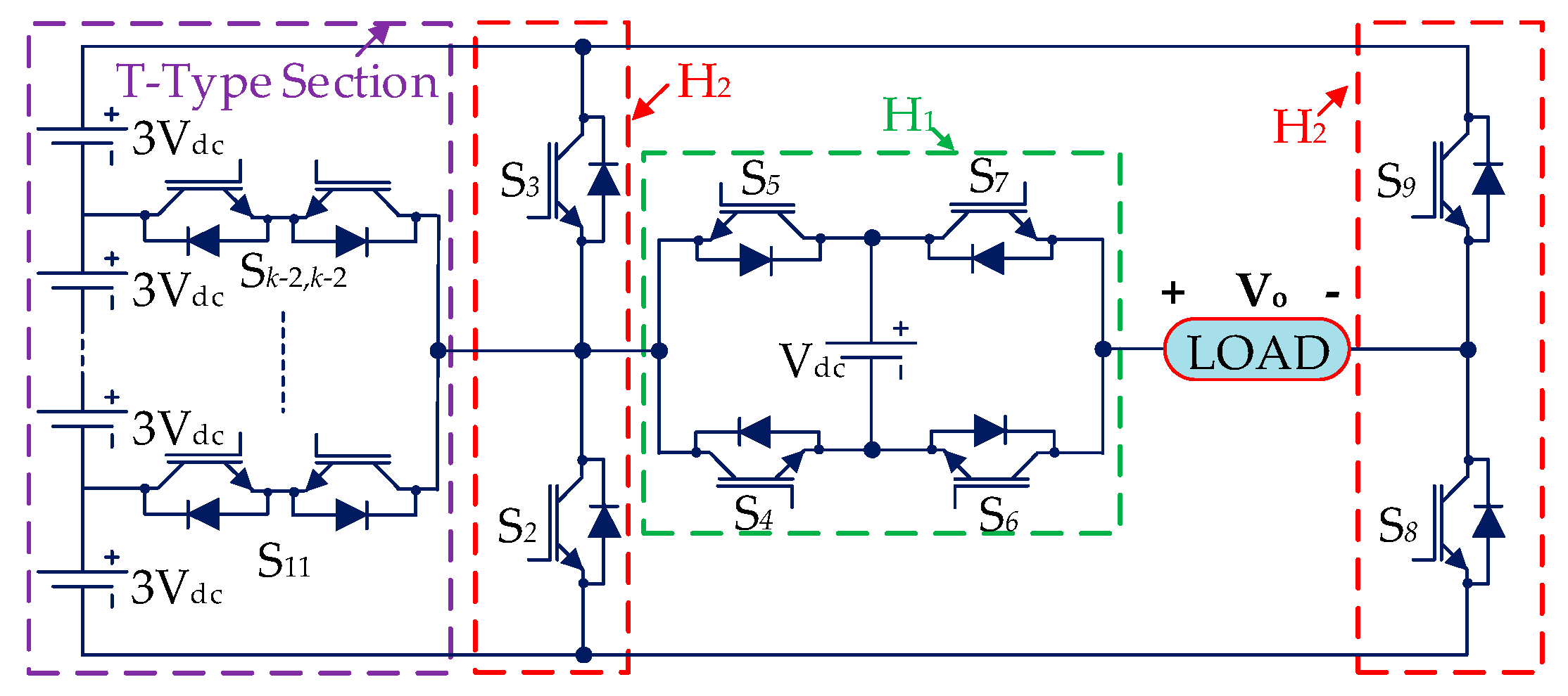
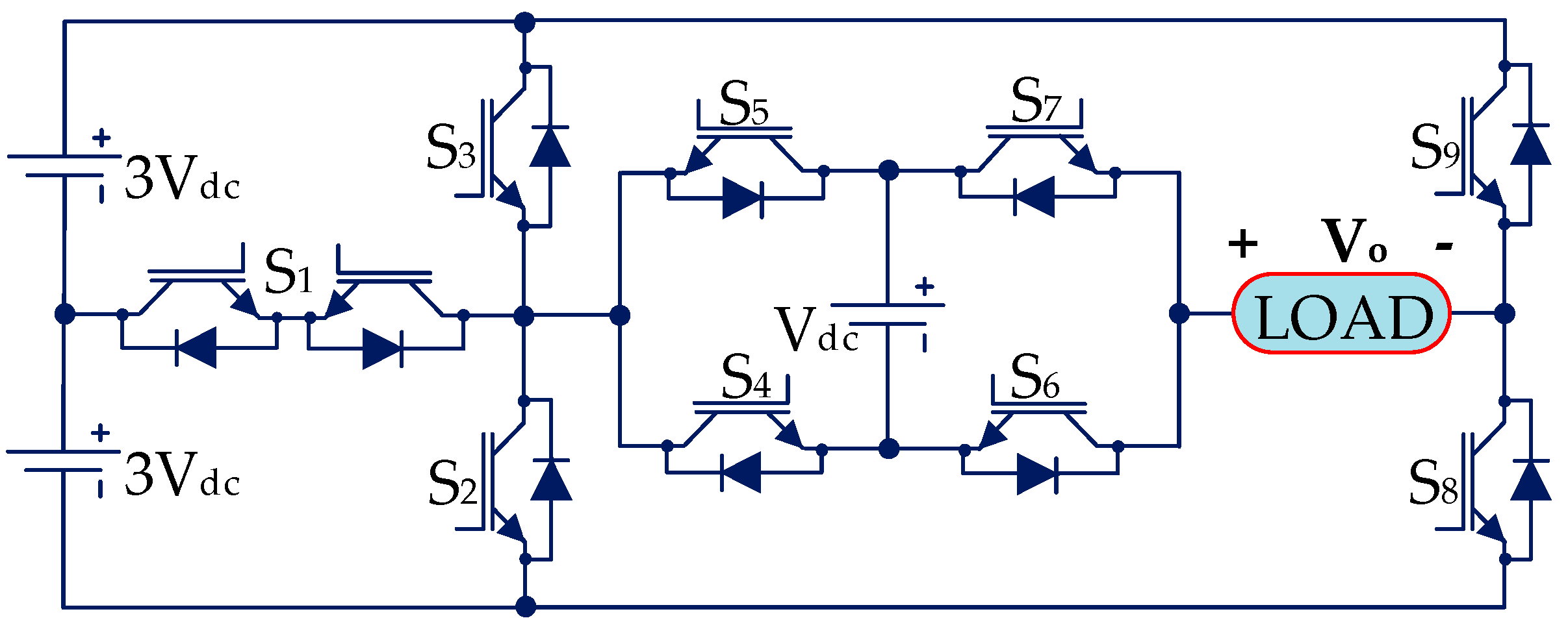
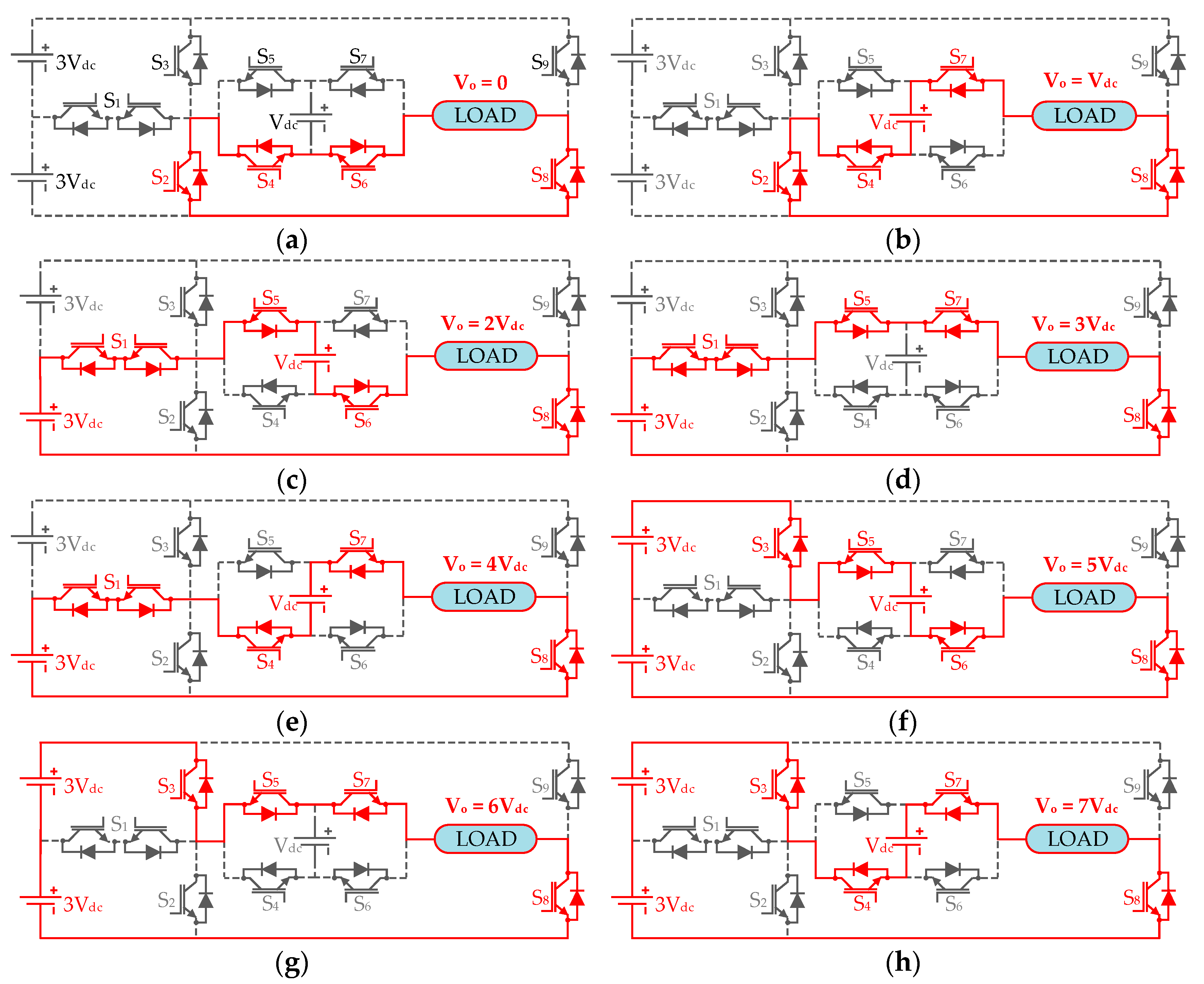
2.1. Basic Unit of the Proposed Topology

Figure 1 depicts the circuit diagram of the basic unit of the proposed multilevel inverter topology. As shown in Figure 1, the basic unit consists of eight unidirectional switches and one bidirectional switch with three dc voltage sources. Two dc voltage sources with a magnitude of 3Vdc are connected on the left-hand side of the basic unit. These two dc voltage sources along with the bidirectional switch S1 form the T-type section of the proposed basic unit. The T-type section is operated at a high voltage and a low frequency. The switches S2–S9 form two H-bridges, i.e., one H-bridge (H1) formed by S2, S3, S8, and S9 and remaining switches S4–S7 form the other H-bridge (H2) with a dc voltage source with a magnitude of Vdc. H1 works at the low switching frequency and H2 operates at the high switching frequency. The load is connected between these two H-bridges. Therefore, the proposed topology can be termed as a “Single-T Double H-bridge” (STDH) MLI. The different switching strategy of the proposed STDH-MLI to generate different voltage levels at the output is given in Table 1. Similarly, Figure 2a–h demonstrate the different combinations of switches and dc voltage sources of the basic unit in the positive half cycle.

2.2. Generalized Structure of the Proposed Topology

To increase the number of levels at the output, the suggested basic unit can be extended as shown in Figure 3. This is done by adding more dc voltage sources to the T-type section. Therefore, when adding one dc voltage source, one bidirectional switch needs to be added to the basic unit. The equations for the proposed STDH-MLI with k number of dc voltage sources are given as:
Number   of   Levels = N l e v e l = n = 3 ( 2 k 1 )
Number   of   Switches = N s w i t c h = 2 k + 4
Number   of   Driver   Circuits = N d r i v e r = k + 6
Variety   of   dc   sources = N v a r i e t y = 2

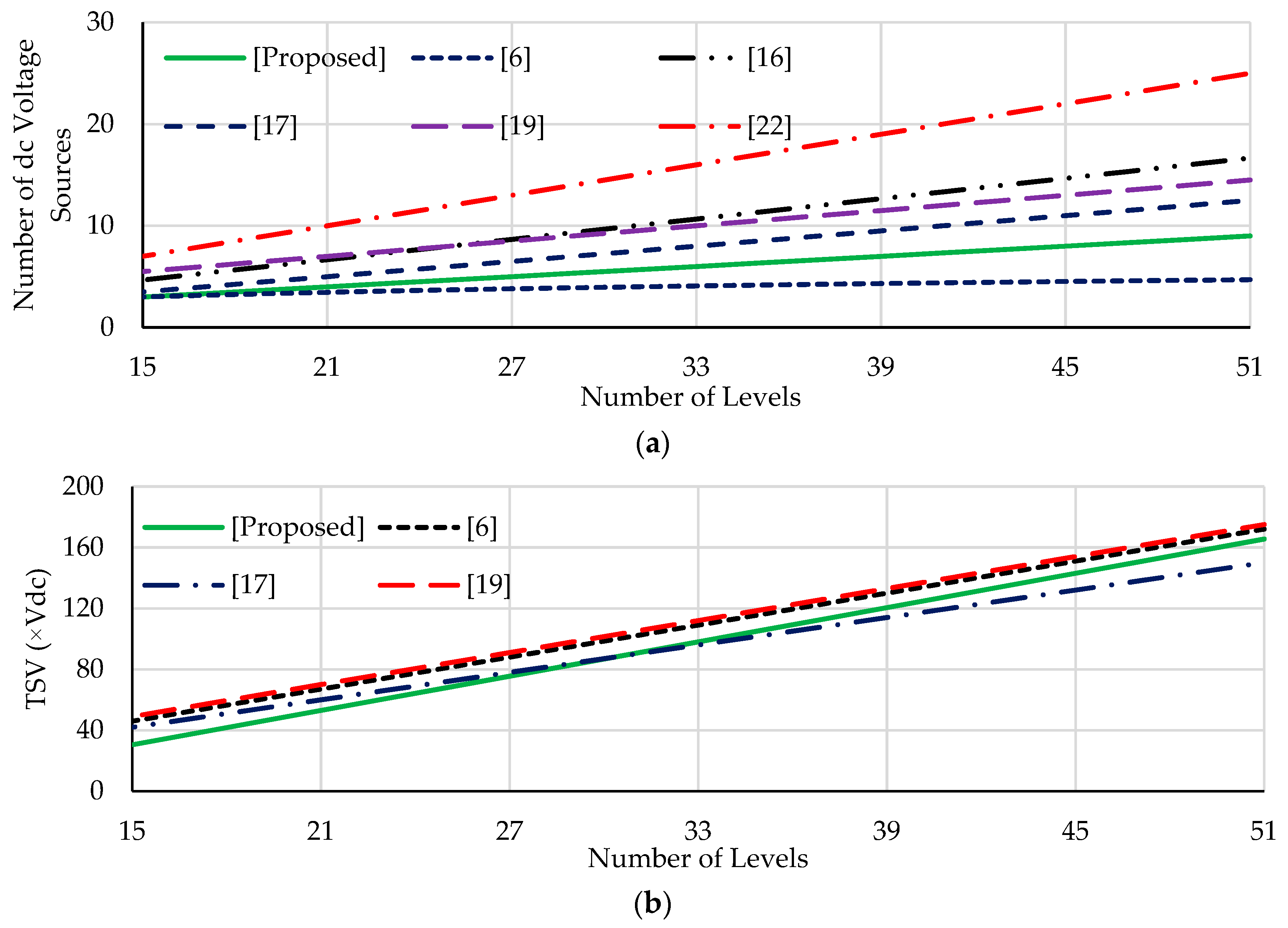
2.3. Calculation of Total Standing Voltage (TSV)

The total standing voltage (TSV) of the topology is an important parameter as it decides the voltage rating of switches to be used in the MLI. TSV is the sum of all the voltage stresses across each switch considering each level at the output. For the proposed STDH-MLI, TSV can be expressed as:
TSV = TSV T + TSV H 1 + TSV H 2
where TSV T is the TSV of the T-section consisting of all bidirectional switches S 11 to S k 2 , k 2 . TSV H 1 and TSV H 2 represent the TSV of H-bridge H1 (made up of S 2 , S 3 , S 8 , and S 9 ) and H-bridge H2 consisting of switches S 4 to S 7 , respectively. TSV T can be calculated as follows:
TSV T = M × 3 V dc
where M in terms of k is given by
M = 3 k 2 4 k + 1 4   for   an   odd   number   of   k M = 3 k 2 4 k 4    for   a   even   number   of   k
The voltage across each switch connected in H1 is (k − 1)V1 as all the switches of H1 are connected to the dc voltage sources connected in the T-section. Therefore,
TSV H 1 = 4 ( k 1 ) × 3 V dc
Similarly,
TSV H 2 = 4 V dc
Therefore, from (6)–(9), total TSV of the proposed MLI is given as:
TSV = ( 3 M + 12 k 8 ) V dc

3. Comparative Study

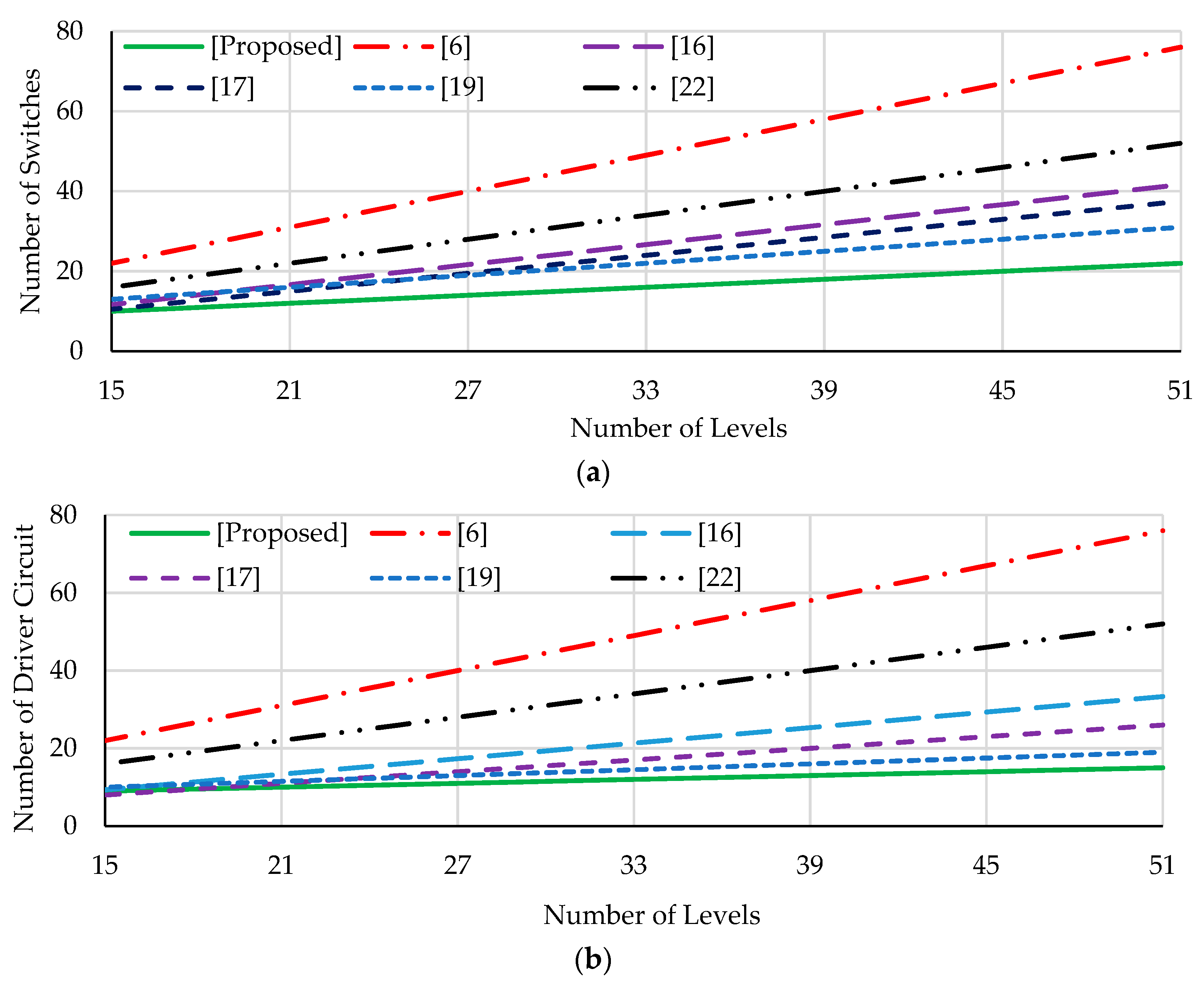
3.1. Comparison of Basic Units

The performance of the proposed basic unit is determined by comparing with it with several new topologies with three dc voltage sources and is given in Table 2. From Table 2, the proposed topology generates the maximum number of levels along with [18], but [18] has higher TSV. TSV is an important factor in the selection of switches. The proposed topology has the least TVS/Nlevel, which appears to be an essential factor for an MLI. In addition, the proposed topology does not use any power diode apart from the antiparallel diodes connected to the switches, which results in a lower amount of losses.

3.2. Comparison of Generalized Structure

The proposed topology can generate any number of levels using the generalized structure. The generalized structure has been compared with some similar MLI topologies to prove the superiority of the proposed topology. The comparison has been carried out in terms of the number of switches, the required number of driver circuits, the number of dc voltage sources, and TSV against the number of levels across the load. Figure 4a presents the variation of number of switches corresponding to the number of levels across the load. The proposed topology requires a lower number of switches with contrast to the other topologies as shown in Figure 4a. As the proposed topology uses bidirectional switches made up of two unidirectional switches connected in a common emitter configuration, the required number of driver circuits is less than the number of switches used in the topology. Figure 4b correlates the required number of driver circuits and the number of levels at the output. The proposed topology uses a minimal number of driver circuits compared to all other topologies used for the comparison.
A figure correlating the number of dc voltage sources with the number of levels across the load is shown in Figure 5a. As shown in the figure, the proposed topology requires a lower number of dc voltage sources except [17]. Similarly, the voltage stress represented as TSV has been shown in Figure 5b. The proposed topology has a lower TSV compared to [6,19]. From this comparison, the proposed topology has a lower number of switches, driver circuits, dc voltage sources, and TSV. The lower number of components along with the lower amount of TSV gives an upper edge to the proposed topology for low- and medium-voltage applications. The lower number of components also reduces the cost and size of the proposed topology.

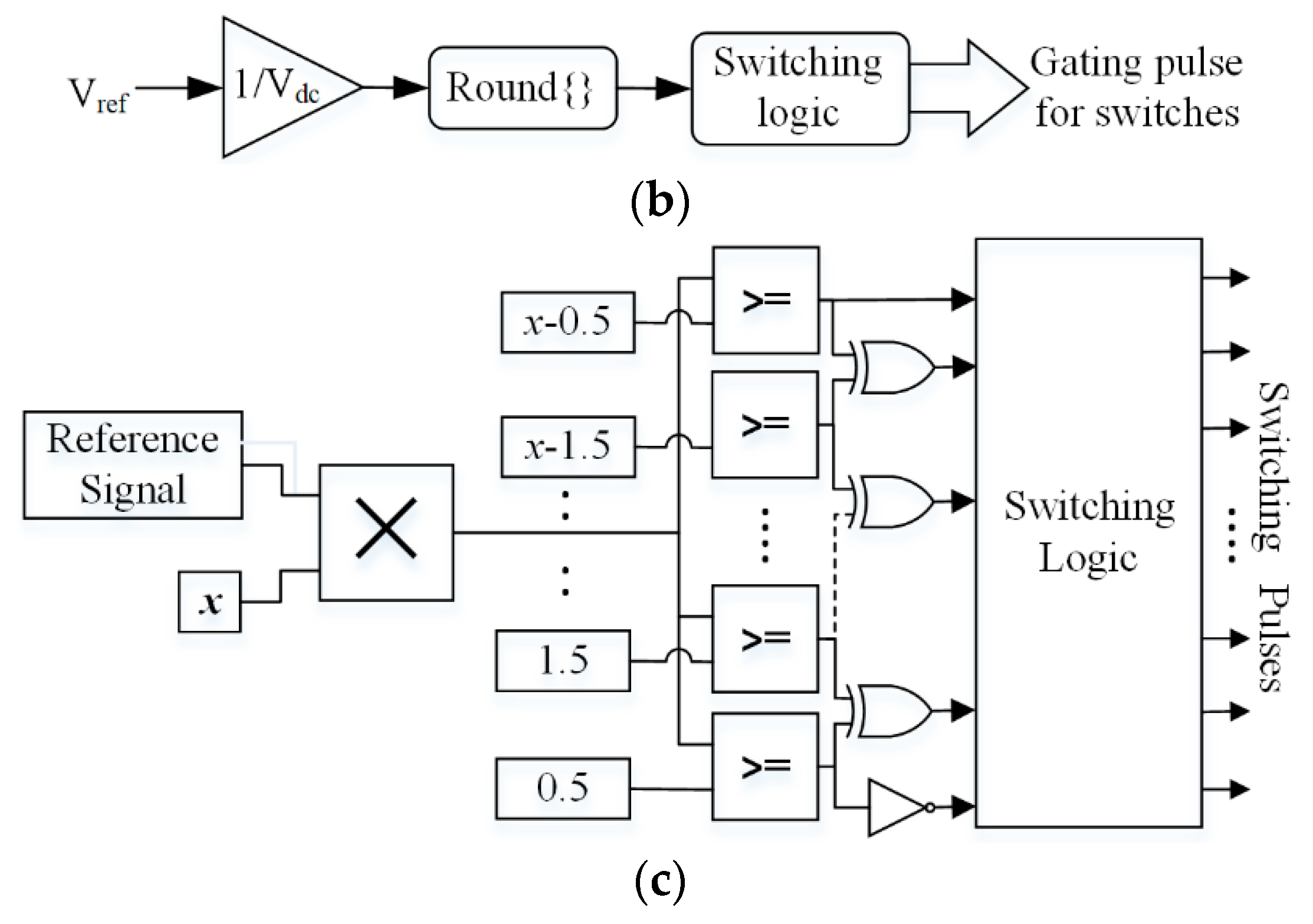
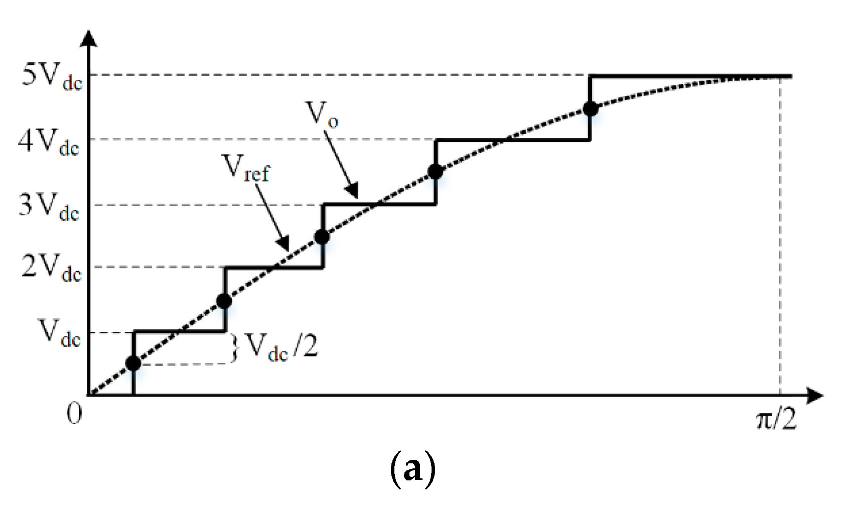
4. Nearest Level Control Modulation Method

Several modulation techniques have been researched and applied to multilevel inverters, such as carrier-based (CB) PWM, Space Vector (SV) PWM, and selective harmonic elimination (SHE) PWM. CBPWM techniques use multiple carrier signals to generate gate pulses but cause higher switching losses. In SVPWM, the complexity of the algorithm increases as the number of levels at the output increases. Likewise, with SHEPWM, the calculation of switching angles becomes more and more complex with increases in the number of levels [29,30,31,32]. The nearest level control (NLC) is a low-switching-frequency PWM technique [33]. In the NLC method, the calculation time is reduced with the complexity in the implementation with an increase in the number of levels compared to SVPWM and SHEPWM. In this method, the sampled waveform can be generated by comparing the sinusoidal reference signal with the existing voltage level at the output as shown in Figure 6a. Figure 6b shows the general control diagram for the NLC. A simplified NLC implementation scheme is given in Figure 6c, where x = (n − 1)/2. The reference signal is multiplied by x to obtain the amplified signal. This signal is compared with different constant dc lines to generate the pulses, and a switching logic is used to combine different pulses to generate the switching pulses for the different switches.

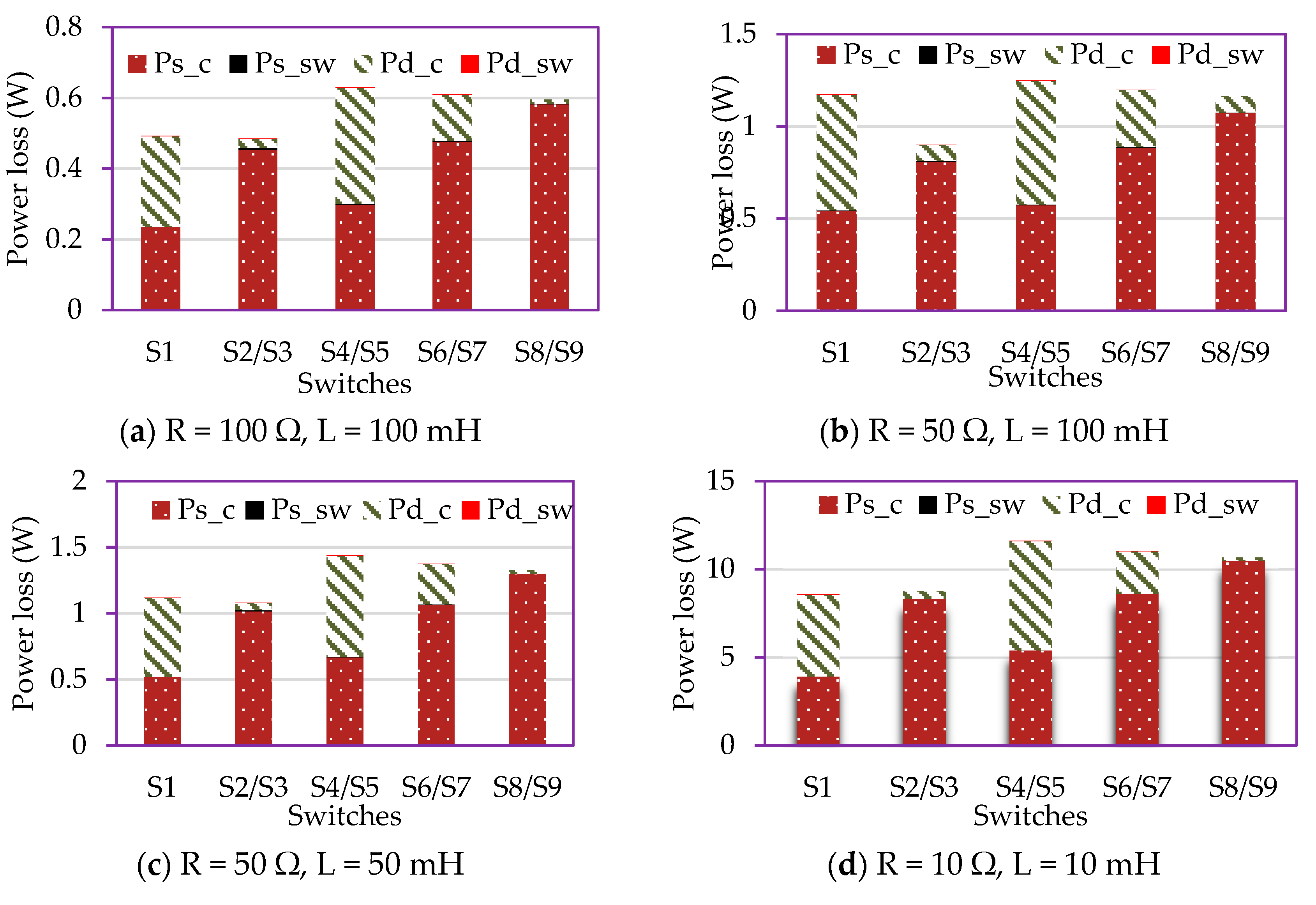
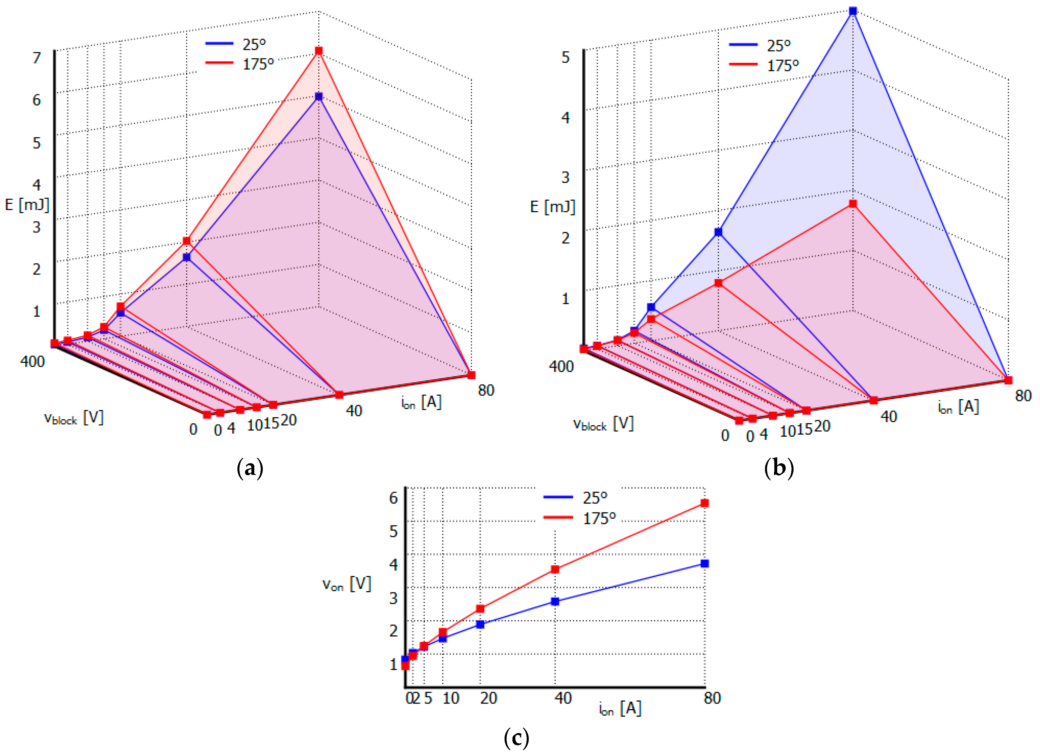
5. Power Loss Analysis

For any power converter with power semiconductor devices, two major losses take place, namely conduction loss (Pc) and switching loss (Psw) [27]. Equivalent resistance and On-state voltage drop of devices are the main factors that decide the amount of conduction loss. The conduction loss for a switch ( P c S ) and its antiparallel diode ( P c d ) is calculated as follows:
P c S = V S O N i ( t ) + R s i β ( t )
P c d = V d O N i ( t ) + R d i 2 ( t )
where V S O N and V d O N represent the On-state voltage drop of the switch and its antiparallel diode, respectively. R s and R d are the equivalent resistance of the switch and diode, respectively, and the constant β depends upon the different parameters of the switch. All these factors associated with the conduction losses can be found from the datasheet of the switch. The average conduction loss for a fundamental period (2π) is calculated as:
P c = x = 1 N s 1 2 π 0 2 π ( V S O N i ( t ) + R s i β ( t ) ) d t + x = 1 N d 1 2 π 0 2 π ( V d O N i ( t ) + R d i 2 ( t ) ) d t .
Switching losses are another type of losses associated with semiconductor devices. Switching losses occur due to the non-ideal operations of the power semiconductor devices. To calculate switching losses, it is assumed that the voltage and current during turn-ON and turn-OFF vary linearly. Thus
P s w = [ x = 1 N s ( N O N x E O N x + N O F F x E O F F x ) ] × f
where N O N x and N O F F x represent the number of turn-ONs and turn-OFFs during one complete cycle for the xth switch. E O N x and E O F F x are the energy losses during turn-ON and turn-OFF in one complete cycle for the xth switch and its anti-parallel diode, respectively, and f represents the fundamental frequency of the output voltage. Therefore, total losses (Pt) is the sum of both conduction and switching losses, given by
P t = P c + P s w .
Therefore, the efficiency ( η ) of the converter with output power Po is given by
η = P o P o + P t × 100 % .
The PLECS software has been used for the calculation of power loss of the semiconductor devices of the proposed topology. The thermal modeling of the proposed topology has been simulated using the parameters of the IGBT switch IKW20N60H3. The energy losses EON and EOFF are associated with the ON-state current and OFF-state blocking voltages. For the selected IGBT, the curves of energy loss with respect to the ON-state current (iON) and OFF-state blocking voltage (Vblock) are given in Figure 7. Figure 7a,b show the curve of energy loss for turn-ON losses and turn-OFF losses, respectively. Figure 7c relates the ON-state voltage drop with ON-state current and it is used for the calculation of the conduction losses.
Figure 8a shows the efficiency of the proposed converter with respect to the output power Po. The estimated efficiency of the proposed converter comes out to be 97.8% at the output power of 50 W. The efficiency of the output power at 5 kW was found to be 93.7%. Furthermore, the proposed topology has been compared with the topology proposed in [18] in terms of efficiency and the results are shown in Figure 8b. To estimate the efficiency, NLCPWM was used with the same peak voltage for both topologies. It is clear from Figure 8b that the efficiency of the proposed topology is better compared to [18].
In terms of efficiency, the proposed topology has been analyzed with both low- and high-switching-frequency techniques. For the low-switching frequency, NLC is used and for the high-switching frequency, sinusoidal PWM (SPWM) is used with the in-phase disposition configuration of the carrier signals. Figure 9a–d show the output voltage waveform of the proposed topology with different switching frequencies and NLCPWM. For SPWM, the carrier frequency has been selected as 5 kHz, 2.5 kHz, and 1 kHz, and the respective 15-level output voltage is depicted in Figure 9a–c, respectively. Figure 9d shows the output voltage waveform with NLCPWM. For all the above four cases, the efficiency has been calculated and the different efficiency versus output power curves are shown in Figure 10. As shown in Figure 10, the proposed topology with NLC gives improved efficiency compared to SPWM.
In addition, the power loss distribution across the different switches has also been analyzed for the proposed topology with different loading conditions with NLCPWM. Figure 11a–d show the switching and conduction losses of different switches and their antiparallel diodes for different loading conditions. The power losses across the complementary switches are similar, i.e., switch S2 and S3 have the same conduction and switching losses as both switches operate for an equal duration with the same number of ON and OFF transitions. As the NLCPWM technique is used, the switching loss has a negligible impact on the total power loss, and conduction loss is the major contributor to the overall losses of the proposed topology.

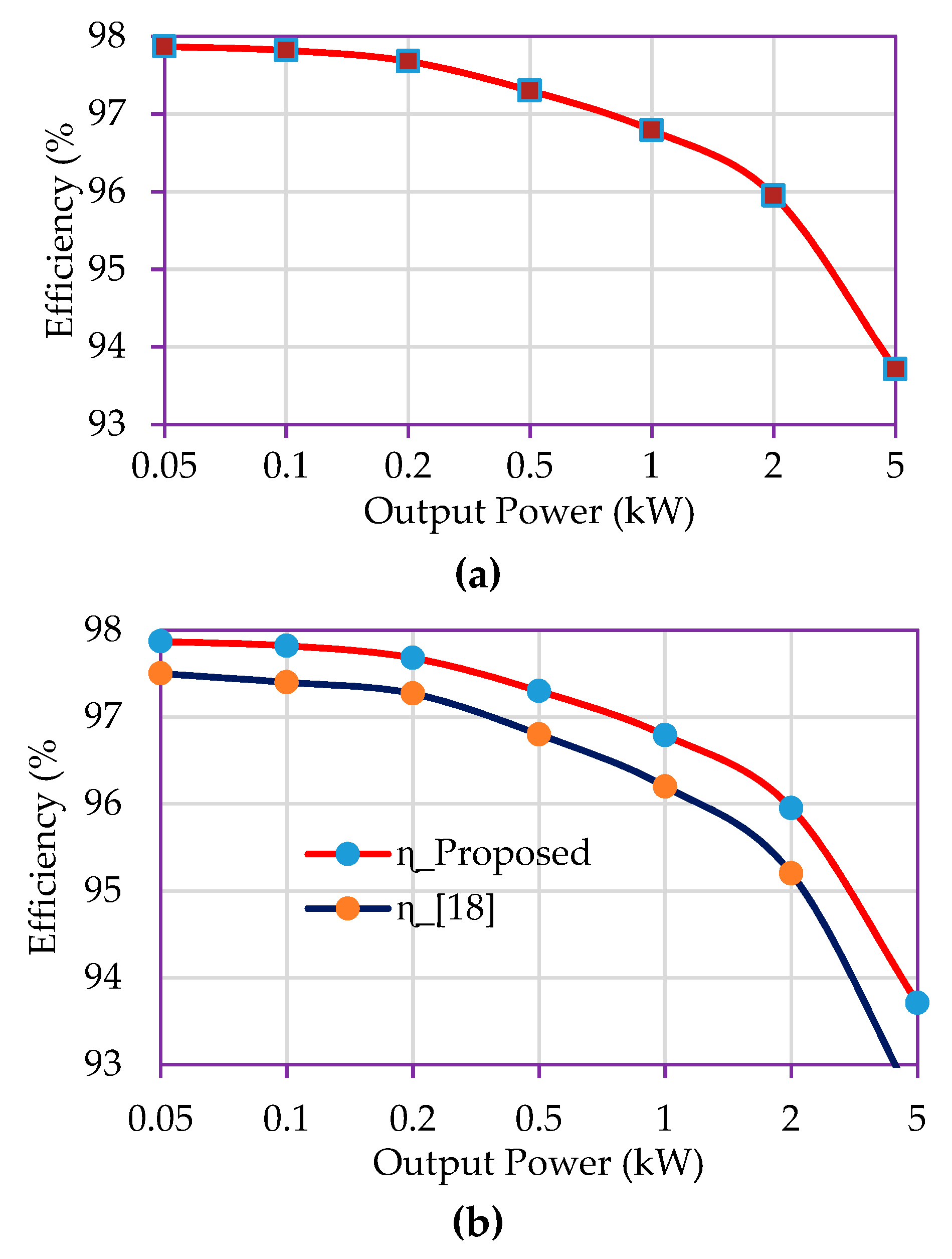
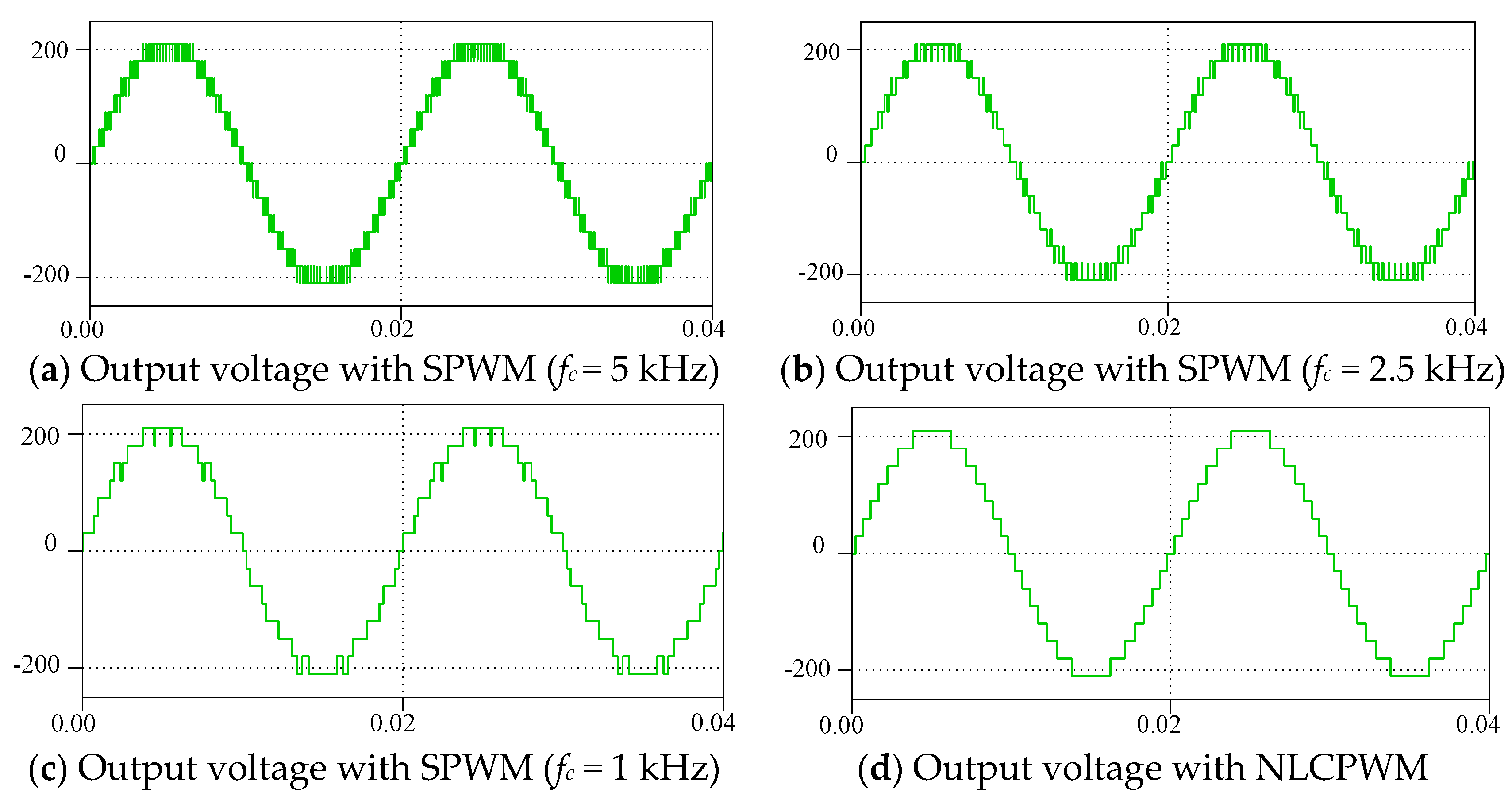
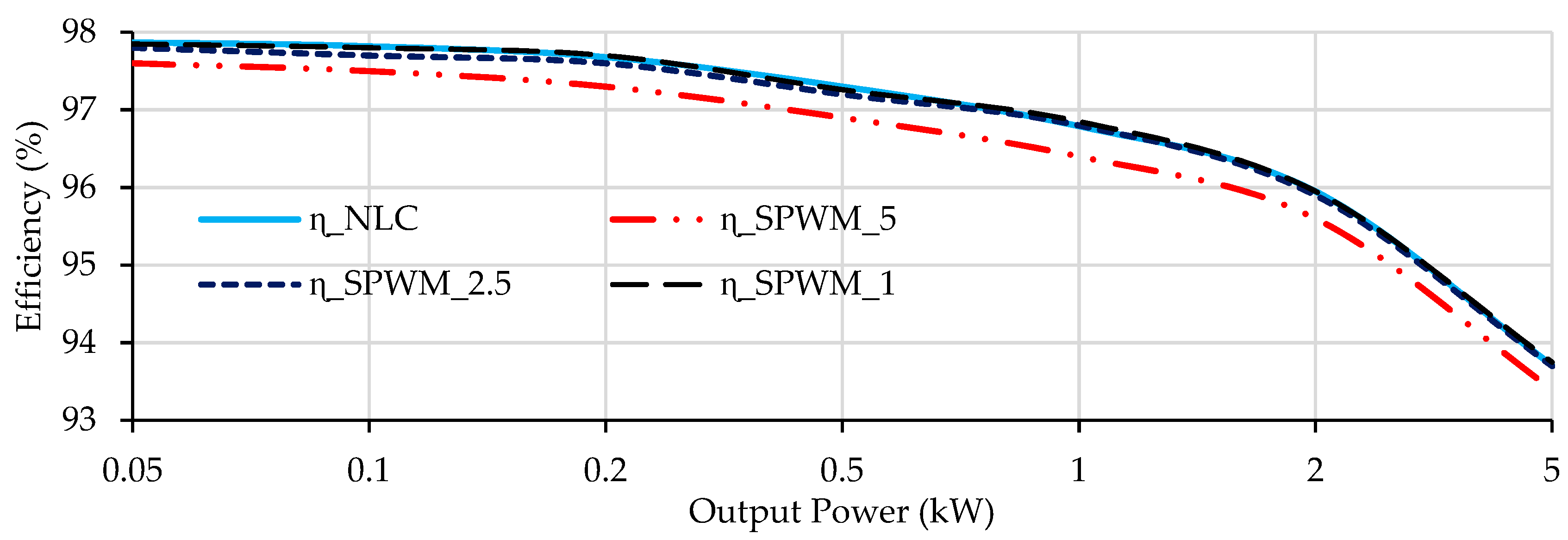
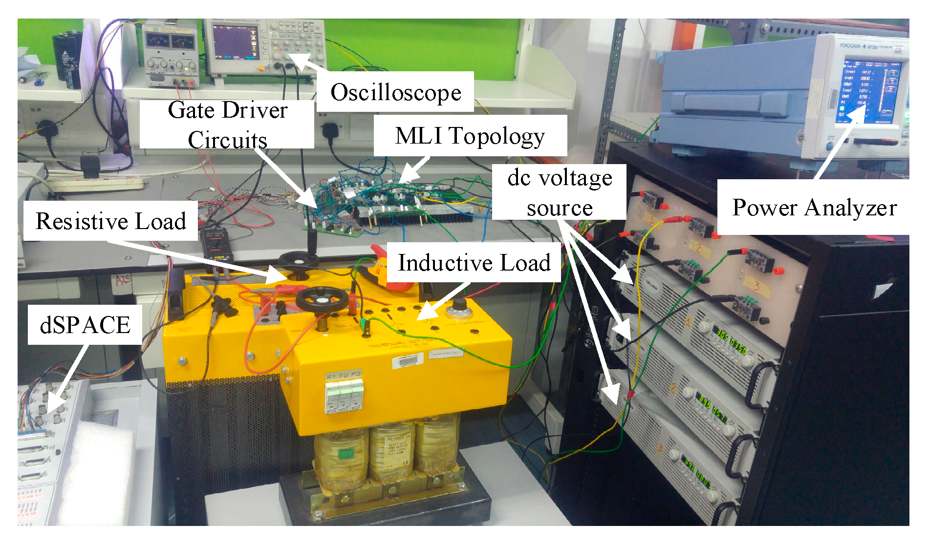
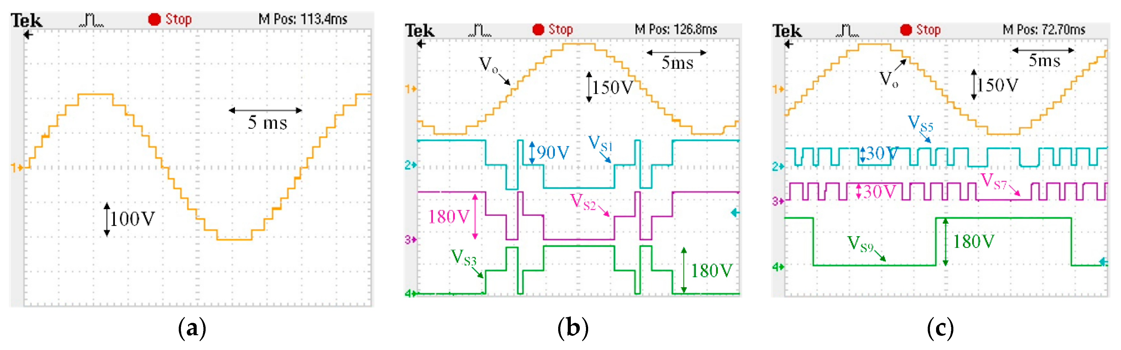
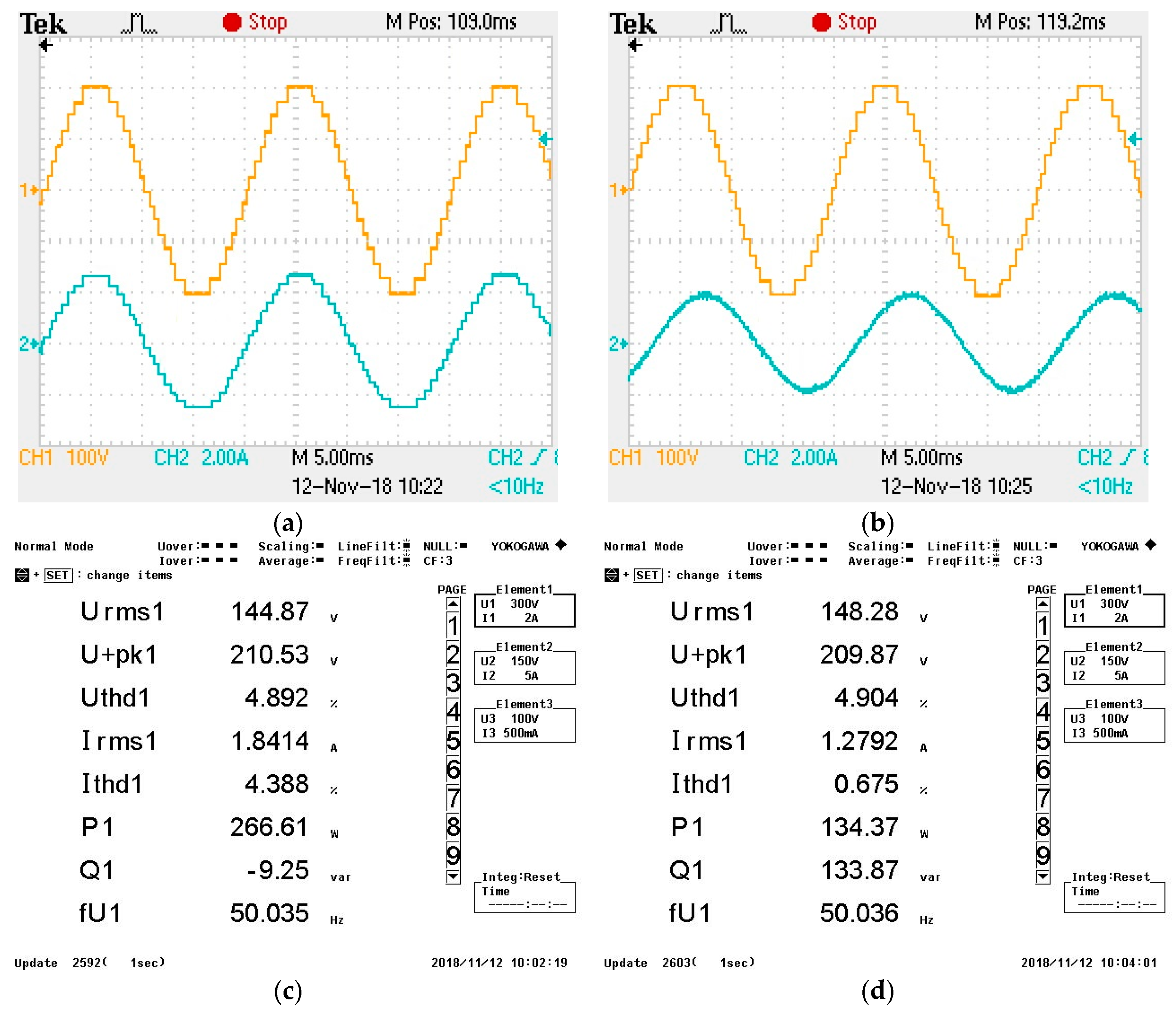
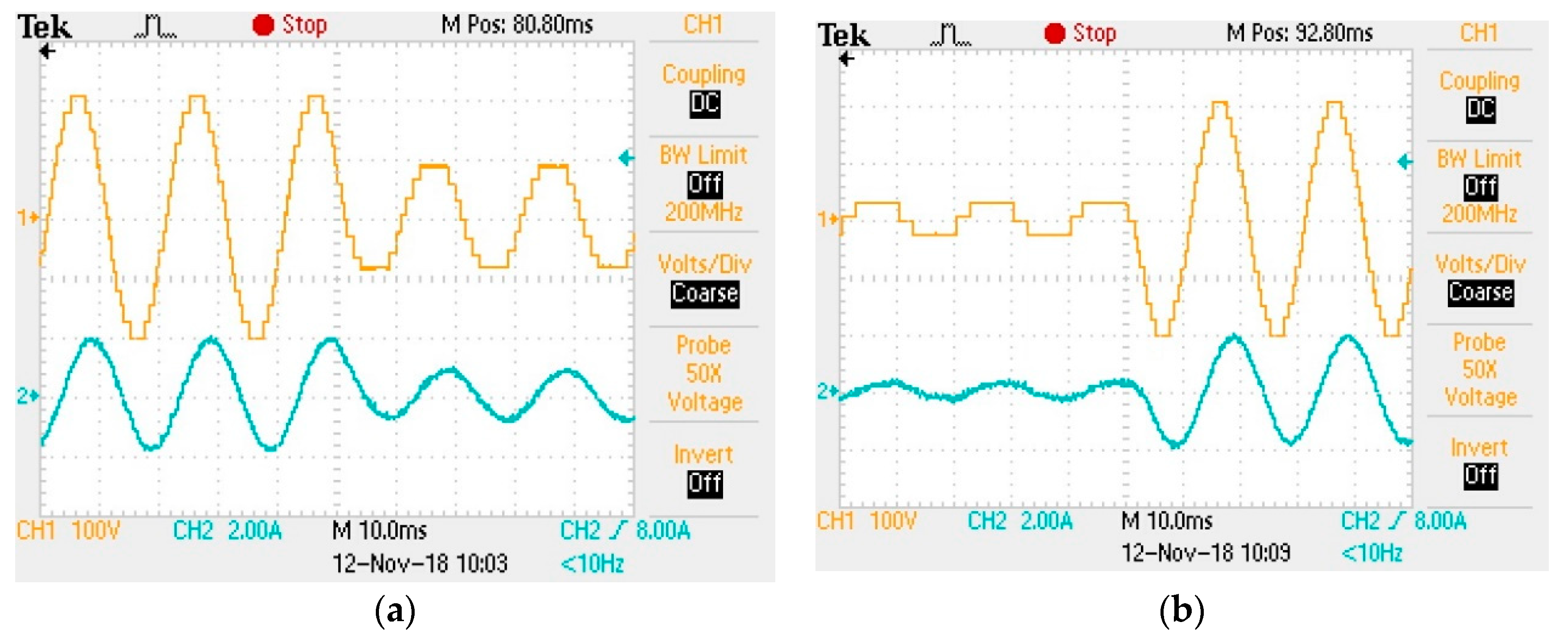
6. Results and Discussion

To verify the performance of the proposed topology, different experimental tests have been performed on the prototype experimental setup as shown in Figure 12. TOSHIBA IGBT GT50J325 has been used as a switch for the topology. dSPACE CP1104 has been used to generate the gate pulses for all the switches using the NLC method described in Section 4. The gate drive circuits, made up of an NXP 74HC04N IC and an A3120 optocoupler, have been used to make the gate pulses suitable for proper IGBT operation.
A different test has been performed for the basic unit, which generates 15 levels across the load. The magnitude of the dc voltage source connected to the T-section has been selected as 90 V, and the magnitude of the dc voltage source connected to H2 has been fixed to 30 V. This selection of dc voltage sources results in an output voltage having a peak magnitude of 210 V with a 30 V voltage step (Vdc = 30 V) as shown in Figure 13a.
The voltages stress across the switches has a crucial role in the design of an MLI topology. For the proposed basic unit, the voltage stress across switches has been analyzed and is shown in Figure 13b,c). The voltage stress across the bidirectional switch S1 is shown in Figure 13b, which varies from zero to 90 V, i.e., 3 Vdc. The switches connected to H1 (S2, S3, S8, and S9) have a maximum voltage stress equal to 6 Vdc, i.e., 180 V. The voltage stress across switches S2 and S3 is shown in Figure 13b. Similarly, for the switches of H2 (S4 to S7), the maximum voltage stress has been fixed to Vdc, i.e., 30 V. The voltage stress across switches S5 and S7 along with the voltage stress of switch S9 are demonstrated in Figure 13c.
The proposed basic unit has been tested under different loading conditions and the results are shown in Figure 14 and Figure 15. Figure 14a depicts the output voltage and current waveform with a purely resistive load having a magnitude of 100 Ω. With the resistive load, the current waveform is in phase with the voltage waveforms as shown in Figure 14a. The different output parameters captured by the power analyzer are provided in Figure 14b. For the 15-level output voltage with resistive load, the voltage total harmonic distortion (THD) is 4.9% and the current THD has a similar magnitude to the voltage THD. Furthermore, the output voltage and current waveforms with the series connected resistive-inductive (RL) load are shown in Figure 14c. The values of resistance and inductance have been selected as R = 100 Ω and L = 200 mH, respectively. With this load, the different output parameters are given in Figure 14d.
Additionally, the proposed topology has been analyzed with the change in the modulation indexes with a load of R = 100 Ω, L = 200 mH. Figure 15a shows the output voltage and current for the change in modulation index from 1.0 to 0.5 with RL load. Similarly, a change in modulation index from 0.2 to 1.0 is provided in Figure 15b. From all these figures, the proposed topology performs well under different loading conditions along with a change in the modulation indexes.

7. Conclusions

This paper presents the working concept of the proposed STDH-MLI, which is a hybrid combination of one T-Type section and two H-Bridges. The basic unit of the proposed topology is able to generate 15 levels at the output employing three dc voltage sources. Moreover, the expansion of the basic unit has been deliberated on with the mathematical formulation of the topology. A comparison with existing topologies approves the merit of the proposed topology in terms of ability to achieve a higher number of levels with a lower TSV using a low number of switches and total components. Finally, the performance of the proposed STDH-MLI is verified through several experimental results using the NLCPWM method.

Author Contributions

M.R. and M.D.S. have contributed to the theoretical approaches, simulation, experimental tests, and preparation of the article, and have contributed equally to this work. S.M. and N.M.S. have contributed to the theoretical approaches, simulations, experimental tests, and preparation of the article. H.B., M.S., B.H. and A.S. have contributed to the theoretical approaches and prepartion of the article.

Funding

This work was supported by the Deanship of Scientific Research (DSR), King Abdulaziz University, Jeddah, under grant No. (D-123-135-1438). The authors, therefore, gratefully acknowledge the DSR technical and financial support.

Conflicts of Interest

The authors declare no conflict of interest.

References

  1. Kouro, S.; Malinowski, M.; Gopakumar, K.; Pou, J.; Franquelo, L.G.; Wu, B.; Rodriguez, J.; Pérez, M.A.; Leon, J.I. Recent Advances and Industrial Applications of Multilevel Converters. IEEE Trans. Ind. Electron. 2010, 57, 2553–2580. [Google Scholar] [CrossRef]
  2. Rodríguez, J.; Lai, J.S.; Peng, F.Z. Multilevel inverters: A survey of topologies, controls, and applications. IEEE Trans. Ind. Electron. 2002, 49, 724–738. [Google Scholar] [CrossRef]
  3. Akagi, H. Multilevel Converters: Fundamental Circuits and Systems. Proc. IEEE 2017, 105, 2048–2065. [Google Scholar] [CrossRef]
  4. Gupta, K.K.; Ranjan, A.; Bhatnagar, P.; Sahu, L.K.; Jain, S. Multilevel Inverter Topologies With Reduced Device Count: A Review. IEEE Trans. Power Electron. 2016, 31, 135–151. [Google Scholar]
  5. Venkataramanaiah, J.; Suresh, Y.; Panda, A.K. A review on symmetric, asymmetric, hybrid and single DC sources based multilevel inverter topologies. Renew. Sustain. Energy Rev. 2017, 76, 788–812. [Google Scholar] [CrossRef]
  6. Hinago, Y.; Koizumi, H. A Single-Phase Multilevel Inverter Using Switched Series/Parallel DC Voltage Sources. IEEE Trans. Ind. Electron. 2010, 57, 2643–2650. [Google Scholar]
  7. Kang, S.H.; Lee, F.S. A new structure of H-bridge multilevel inverter. In Proceedings of the Annual Fall Conference of Power Electronics (KIPE Conference), Goyang, Korea, 31 October 2008; pp. 388–390. [Google Scholar]
  8. Choi, W.K.; Kang, F.S. H-bridge based multilevel inverter using PWM switching function. In Proceedings of the INTELEC 2009-31st International Telecommunications Energy Conference, Incheon, Korea, 18–22 October 2009. [Google Scholar]
  9. Samsami, H.; Taheri, A.; Samanbakhsh, R. New bidirectional multilevel inverter topology with staircase cascading for symmetric and asymmetric structures. IET Power Electron. 2017, 10, 1315–1323. [Google Scholar] [CrossRef]
  10. Ebrahimi, J.; Babaei, E.; Gharehpetian, G.B. A New Multilevel Converter Topology With Reduced Number of Power Electronic Components. IEEE Trans. Ind. Electron. 2012, 59, 655–667. [Google Scholar] [CrossRef]
  11. Babaei, E.; Laali, S.; Bayat, Z. A Single-Phase Cascaded Multilevel Inverter Based on a New Basic Unit With Reduced Number of Power Switches. IEEE Trans. Ind. Electron. 2015, 62, 922–929. [Google Scholar]
  12. Jammala, V.; Yellasiri, S.; Panda, A.K. Development of a New Hybrid Multilevel Inverter Using Modified Carrier SPWM Switching Strategy. IEEE Trans. Power Electron. 2018, 33, 8192–8197. [Google Scholar]
  13. Yu, H.; Chen, B.; Yao, W.; Lu, Z. Hybrid Seven-Level Converter Based on T-Type Converter and H-Bridge Cascaded under SPWM and SVM. IEEE Trans. Power Electron. 2018, 33, 689–702. [Google Scholar] [CrossRef]
  14. Wang, K.; Zheng, Z.; Wei, D.; Fan, B.; Li, Y. Topology and Capacitor Voltage balancing Control of a Symmetrical Hybrid Nine-Level Inverter for High Speed Motor Drives. IEEE Trans. Ind. Appl. 2017, 53, 5563–5572. [Google Scholar] [CrossRef]
  15. Roy, J.; Chamarthi, P.; Agarwal, V. A hybrid 9-level inverter with minimum number of switches for single phase grid connected solar PV system. In Proceedings of the 43rd Photovoltaic Specialists Conference (PVSC), Portland, OR, USA, 5–10 June 2016; pp. 3252–3257. [Google Scholar]
  16. Samadaei, E.; Gholamian, S.A.; Sheikholeslami, A.; Adabi, J. An Envelope Type (E-Type) Module: Asymmetric Multilevel Inverters With Reduced Components. IEEE Trans. Ind. Electron. 2016, 63, 7148–7156. [Google Scholar] [CrossRef]
  17. Samadaei, E.; Sheikholeslami, A.; Gholamian, S.-A.; Adabi, J. A Square T-Type (ST-Type) Module for Asymmetrical Multilevel Inverters. IEEE Trans. Power Electron. 2017, 99, 987–996. [Google Scholar] [CrossRef]
  18. Su, G.-J. Multilevel DC-Link Inverter. IEEE Trans. Ind. Appl. 2005, 41, 848–854. [Google Scholar] [CrossRef]
  19. Jayabalan, M.; Jeevarathinam, B.; Sandirasegarane, T. Reduced switch count pulse width modulated multilevel inverter. IET Power Electron. 2017, 10, 10–17. [Google Scholar] [CrossRef]
  20. Gautam, S.P.; Gupta, S.; Sahu, L.K. Reduction in number of devices for symmetrical and asymmetrical multilevel inverters. IET Power Electron. 2016, 9, 698–709. [Google Scholar] [CrossRef]
  21. Odeh, C.I.; Obe, E.S.; Ojo, O. Topology for cascaded multilevel inverter. IET Power Electron. 2016, 9, 921–929. [Google Scholar] [CrossRef]
  22. Ounejjar, Y.; Al-Haddad, K.; Grégoire, L.A. Packed U cells multilevel converter topology: Theoretical study and experimental validation. IEEE Trans. Ind. Electron. 2011, 58, 1294–1306. [Google Scholar] [CrossRef]
  23. Shueai Alnamer, S.; Mekhilef, S.; Bin Mokhlis, H. A Four-Level T-Type Neutral Point Piloted Inverter for Solar Energy Applications. Energies 2018, 11, 1546. [Google Scholar] [CrossRef]
  24. Bassi, H.; Salam, Z. A New Hybrid Multilevel Inverter Topology with Reduced Switch Count and dc Voltage Sources. Energies 2019, 12, 977. [Google Scholar] [CrossRef]
  25. Siddique, M.D.; Mekhilef, S.; Shah, N.M.; Memon, M.A. Optimal Design of a New Cascaded Multilevel Inverter Topology with Reduced Switch Count. IEEE Access 2019, 7, 24498–24510. [Google Scholar] [CrossRef]
  26. Siddique, M.D.; Mustafa, A.; Sarwar, A.; Mekhilef, S.; Shah, N.B.M.; Seyedamahmousian, M.; Stojcevski, A.; Horan, B.; Ogura, K. Single phase symmetrical and asymmetrical design of multilevel inverter topology with reduced number of switches. In Proceedings of the 2018 IEEMA Engineer Infinite Conference (eTechNxT), Greater Noida, NCR of Delhi, India, 13–14 March 2018; pp. 1–6. [Google Scholar]
  27. Thiruvengadam, A. An Enhanced H-Bridge Multilevel Inverter with Reduced THD, Conduction, and Switching Losses Using Sinusoidal Tracking Algorithm. Energies 2018, 12, 81. [Google Scholar] [CrossRef]
  28. Aganah, K.; Luciano, C.; Ndoye, M.; Murphy, G.; Aganah, K.A.; Luciano, C.; Ndoye, M.; Murphy, G. New Switched-Dual-Source Multilevel Inverter for Symmetrical and Asymmetrical Operation. Energies 2018, 11, 984. [Google Scholar] [CrossRef]
  29. Konstantinou, G.; Pou, J.; Ceballos, S.; Darus, R.; Agelidis, V. Switching Frequency Analysis of Staircase Modulated Modular Multilevel Converters and Equivalent PWM Techniques. IEEE Trans. Power Deliv. 2015, 31, 28–36. [Google Scholar] [CrossRef]
  30. Memon, M.A.; Mekhilef, S.; Mubin, M.; Aamir, M. Selective harmonic elimination in inverters using bio-inspired intelligent algorithms for renewable energy conversion applications: A review. Renew. Sustain. Energy Rev. 2018, 82, 2235–2253. [Google Scholar] [CrossRef]
  31. Memon, M.A.; Mekhilef, S.; Mubin, M. Selective harmonic elimination in multilevel inverter using hybrid APSO algorithm. IET Power Electron. 2018, 11, 1673–1680. [Google Scholar] [CrossRef]
  32. Dahidah, M.S.A.; Konstantinou, G.; Agelidis, V.G. A Review of Multilevel Selective Harmonic Elimination PWM: Formulations, Solving Algorithms, Implementation and Applications. IEEE Trans. Power Electron. 2015, 30, 4091–4106. [Google Scholar] [CrossRef]
  33. Meshram, P.M.; Borghate, V.B. A simplified nearest level control (NLC) voltage balancing method for modular multilevel converter (MMC). IEEE Trans. Power Electron. 2015, 30, 450–462. [Google Scholar] [CrossRef]
Figure 1. Basic unit of proposed multilevel inverter topology.
Energies 12 01810 g001
Figure 2. Different switching states of the proposed basic unit in a positive half cycle (a) Vo = 0, (b) Vo = Vdc, (c) Vo = 2Vdc, (d) Vo = 3Vdc, (e) Vo = 4Vdc, (f) Vo = 5Vdc, (g) Vo = 6Vdc, and (h) Vo = 7Vdc.
Energies 12 01810 g002
Figure 3. Generalized structure of the proposed topology.
Energies 12 01810 g003
Figure 4. Variation of (a) number of switches and (b) number of gate driver circuits with respect to number of levels.
Energies 12 01810 g004
Figure 5. Variation of (a) number of dc voltage sources and (b) voltage stress in terms of total standing voltage (TSV) with respect to number of levels.
Energies 12 01810 g005
Figure 6. Nearest level control (NLC) with (a) sampled reference voltage, (b) Implementation of NLC and (c) and simplified NLC implementation.
Energies 12 01810 g006aEnergies 12 01810 g006b
Figure 7. Curves associated with (a) Turn ON losses, (b) Turn OFF losses and (c) Conduction losses.
Energies 12 01810 g007
Figure 8. Estimated efficiency of (a) the proposed topology, and (b) comparison of efficiency of the proposed topology and the topology of [18].
Energies 12 01810 g008
Figure 9. Fifteen-level output voltage with (a) SPWM with fc = 5 kHz, (b) SPWM with fc = 2.5 kHz, (c) SPWM with fc = 1 kHz, and (d) NLCPWM.
Energies 12 01810 g009
Figure 10. The efficiency versus output power curve with different switching frequencies.
Energies 12 01810 g010
Figure 11. Power loss distribution for various loading conditions.
Energies 12 01810 g011
Figure 12. The hardware setup of the proposed topology.
Energies 12 01810 g012
Figure 13. Experiemntal results (a) output voltage waveform of the basic unit, (b) voltage stress across switches S1, S2, and S3 and (c) voltage stress across switches S5, S7, and S9.
Energies 12 01810 g013
Figure 14. (a) The output voltage and current waveform with resistive load with 100 Ω; (b) different output parameters with 100 Ω; (c) the output voltage and current waveform with series connected RL Load with R = 100 Ω, L = 200 mH; and (d) different output parameters with R = 100 Ω, L = 200 mH.
Energies 12 01810 g014
Figure 15. The output voltage and current waveform with a change in the modulation index from (a) 1.0 to 0.5 and (b) 0.2 to 1.0.
Energies 12 01810 g015
Table 1. Switching Table of the Proposed Basic Unit.
S1S2S3S4S5S6S7S8S9Vo
0101010100
010100110Vdc
1000110102Vdc
1000101103Vdc
1001001104Vdc
0010110105Vdc
0010101106Vdc
0011001107Vdc
0010101010
001011001−Vdc
100100101−2Vdc
100101001−3Vdc
100011001−4Vdc
010100101−5Vdc
010101001−6Vdc
010011001−7Vdc
Table 2. Quantitative Comparison of the Basic Unit with Topologies having Three direct current (dc) Voltage Sources.
TopologyABCDETSV (×Vdc)TVS/D
[18]10100153422.80
[19]1290112353.18
[20]77492262.89
[21]77492212.33
Proposed1090152312.07

