Article

Design and Implementation of Finite Time Nonsingular Fast Terminal Sliding Mode Control for a Novel High Step-Up DC-DC Converter

College of Electrical Engineering and Information Technology, Sichuan University, Chengdu 610065, China
*
Author to whom correspondence should be addressed.
Energies 2019, 12(9), 1716; https://doi.org/10.3390/en12091716
Submission received: 1 April 2019 / Revised: 27 April 2019 / Accepted: 28 April 2019 / Published: 7 May 2019
(This article belongs to the Section F: Electrical Engineering)

Abstract

:
In this paper, a new, high step-up quadratic boost converter with high conversion efficiency is discussed. A storage capacitor and resonant inductor are connected in series with a clamp capacitor through a diode. These compose a voltage multiplier cell, which is applied on the switch of the quadratic boost converter. The clamp capacitor can protect the switch from a voltage spike and absorb energy when the switch turns off; then, the storage capacitor and resonant inductor are charged by the energy stored in the clamped capacitor to increase the voltage transfer gain. In addition, the voltage multiplier cell can also reduce the voltage stresses of power devices. Then, a 16 V input, 200 V output prototype with 80 W nominal power is built up and tested. Furthermore, a finite time fast terminal sliding mode (NFTSM) control is proposed, with constant frequency for the voltageFundamental Building B213:tracking control of this converter. The new NFTSM is obtained by introducing an adjustable nonlinear term into fast terminal sliding mode (FTSM) control, and a singularity problem is avoided. The experiment illustrates that the maximum efficiency of the proposed converter achieves 95% at D = 0.25 , V o = 150 V. The voltage stress is reduced to half of the corresponding component of the basic boost converter at the same voltage level. Moreover, the proposed NFTSM controller can track the reference signal, and provide a short settling time of about 48 ms with no overshoot, and the system response exhibits strong robustness against 11.7% input voltage disturbance and 30% load variation.

1. Introduction

Recently, the fast development of electronics products, such as solar energies, uninterruptible power supplies (UPS), and electric automobiles have been witnessed [1,2,3]. DC-DC converters has been wildly applied to these applications. However, due to a low and varying input voltage of these applications, the boost converter is a convenient solution for step-up conversion. However, it is difficult for the conventional converter to provide such a high direct-current (DC) voltage gain. Moreover, many power devices of boost converters suffer from overlarge stress at a high output voltage level, leading to decreased efficiency [4].
Some scholars have strived to increase steady voltage gain and efficiency of boost converters. Some structures, such as the cascaded structure or switched-capacitor [5,6,7] can extend the steady voltage gain at a low cost. However, with the increase of voltage gain, more stages are adopted, leading to a complex circuit and significant current ripple [8]. In some isolated converters [9,10], much high-voltage conversion ratios can be achieved at a relatively low-duty cycle, but the leakage inductor of the magnetic elements may give rise to high voltage spikes and inevitable energy decreases. Furthermore, the volume and weight of power transformers are obstacles for a compact converter. A quadratic boost converter with a single switch can also boost the voltage gain with few components [11]. However, most previous converters may suffer from too much voltage stress, leading to reduced the conversion efficiency. The soft switch techniques [12] can recycle the leakage energy of magnetic elements, but at the price of increasing topology complexity. A voltage multiplier cell is a selectable option [13], which can not only alleviate voltage stress, but also improve the voltage gain.
A control strategy is indispensable to stabilize DC-DC converters against external disturbances. Many classical linear control methods which may achieve mediocre performance cannot even guarantee the stability, owing to the strong nonlinear property of boost converters. Therefore, some nonlinear control strategies, such as neural network control, adaptive control, and sliding mode control (SMC) [14,15,16] have been applied to it. The switch operation on the sliding mode surface of SMC is similar to the two operation states of the DC-DC converter (switch “ON” and “Off”) so that SMC is inherently appropriate to DC-DC converters. Moreover, SMC has characteristics of strong robustness and easy implementation, which is why SMC has generally been used on DC-DC converters. In earlier research, a hysteresis was adopted to relieve chattering and reduce switching frequency [17]. However, the variational switching frequency still exists, which may induce power losses and the electromagnetic interference (EMI) problem. To avoid this disadvantage, a fixed frequency SMC had been proposed [18,19] that can provide a constant operation frequency against external disturbances.
One disadvantage of the lineal sliding mode control is that the system can only converge to the equilibrium points asymptotically, leading to an infinite convergence time theoretically. Afterwards, a terminal sliding mode (TSM) control characterized by a nonlinear sliding mode was developed to guarantee finite-time convergence [20]. It can speed up the convergence rate near the equilibrium point, bringing about improved transient performance. However, this TSM control method cannot deliver a fast convergence speed when the system states have a distance from the equilibrium point. To ensure fast transient convergence in whole state space, a fast terminal sliding mode (FTSM) control was adopted [21]. The FTSM control ensures fast transient convergence in a whole convergence process. However, the previous TSM and FTSM methods may both endure a singularity problem. A few methods have been investigated to overcome this difficulty. One approach is the so-called two-phase control strategy. The trajectory was transferred to a specific region where no singularity occurs. Another approach is to add a saturation function to limit the amplitude of singularity term [22]. It should be noticed that these methods need an extra procedure to eliminate the singularity. In this paper, a novel nonsingular fast terminal sliding mode (NFTSM) is proposed without any additional procedures to avoid the singularity problem.
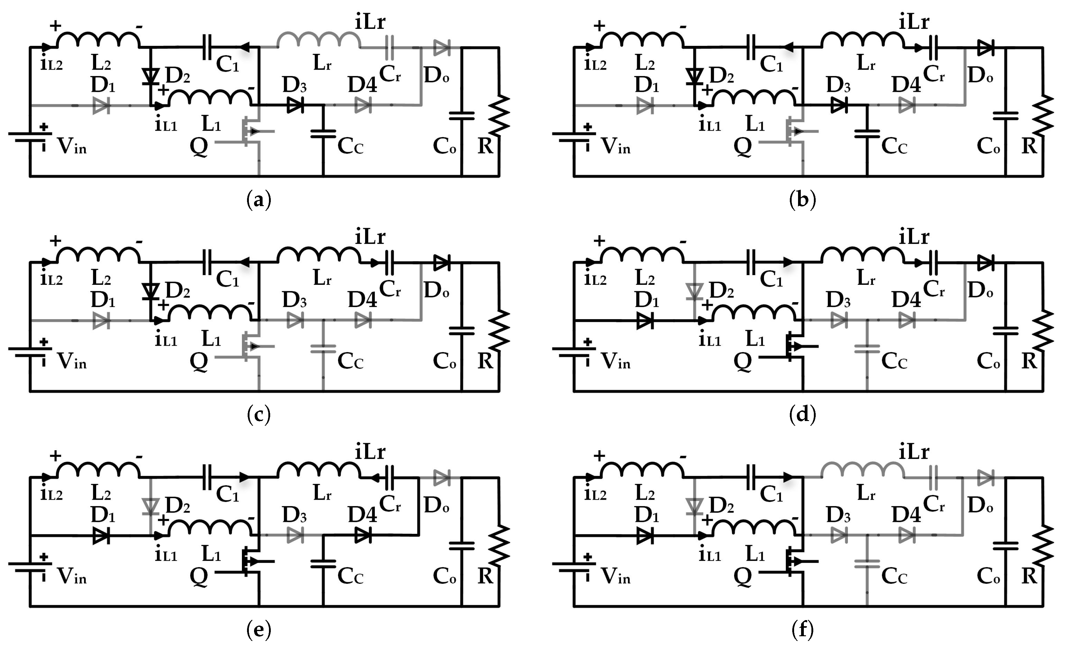
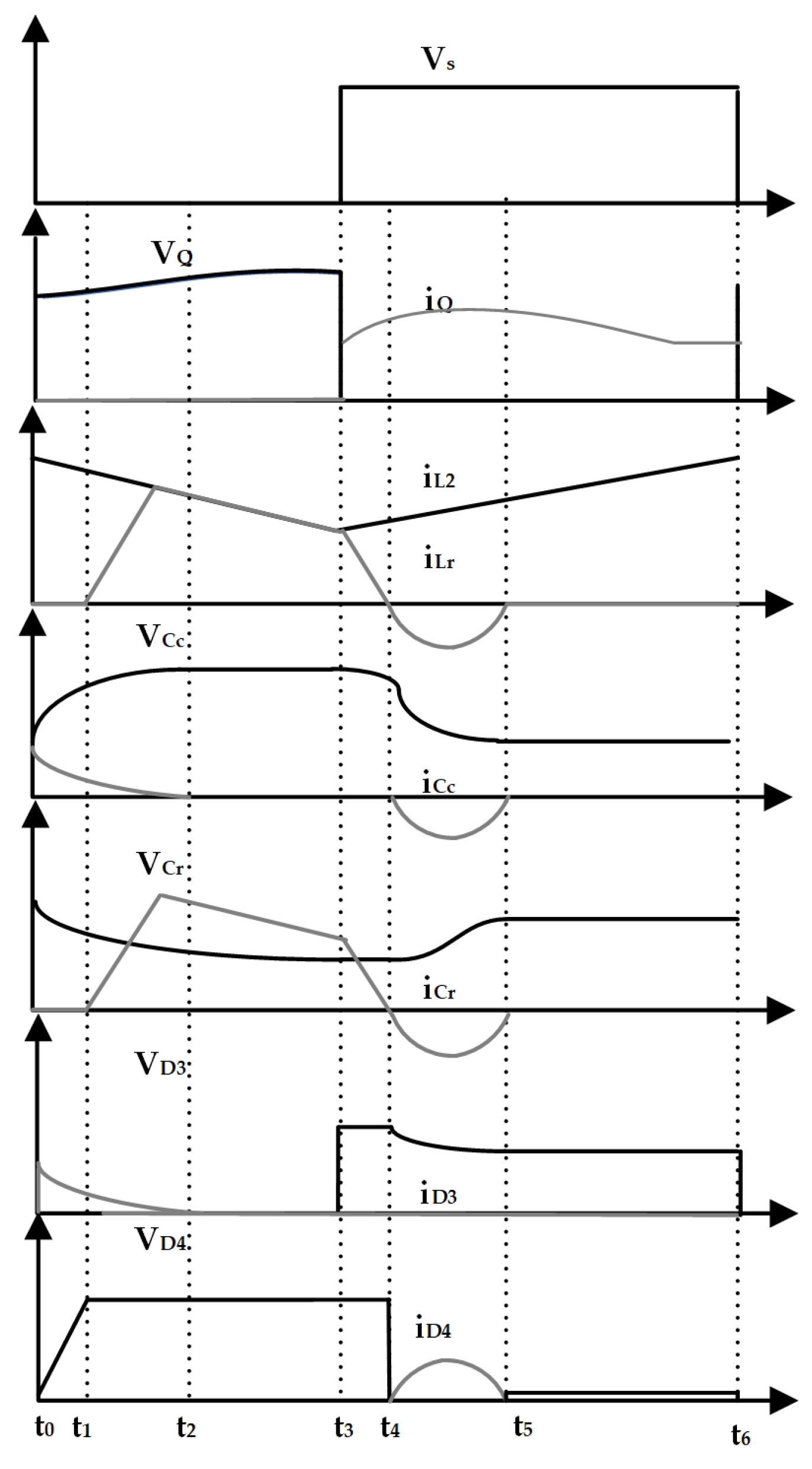
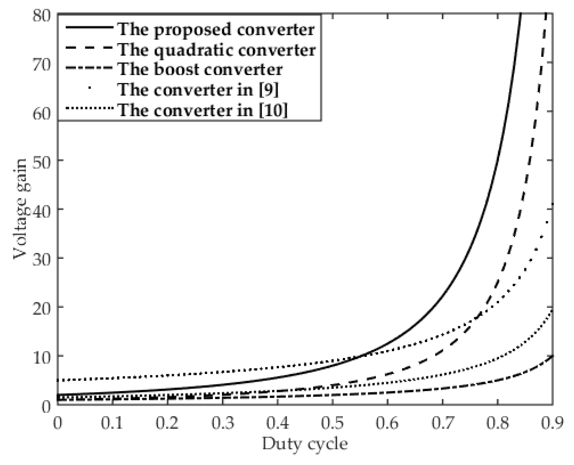
Also in this paper, a new high step-up converter with voltage multiplier is firstly addressed. This scheme is based on a combination of the quadratic boost converter with the voltage multiplier. Secondly, a novel finite-time NFTSM controller is designed for this converter. Finally, the new NFTSM controller is applied onto the proposed converter. Numerical simulations and experiments are provided to illustrate the effectiveness of the novel converter and controller. The arrangement of this paper is given as follows: the operation principle is introduced in Section 2; Section 3 discusses performance and key parameters; the NFTSM controller is designed and analysed in Section 4; the experimental results are introduced in Section 5; then, Section 6 concludes this paper.
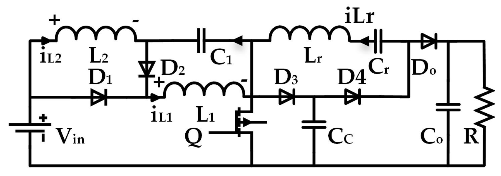
Notations. Throughout this paper, Q is a switch; L 1 , L 2 are input inductors, and L r is a resonant inductor; C 1 , C o , C r , C c are capacitors; D 1 , D 2 , D 3 , D 4 , D o are diodes; and R is a load, respectively. V denotes the voltage of across corresponding element; for example, V Q represents the input voltage, and V D 1 , V D 2 , V D 3 , V D 4 , V D o stand for the voltages across of D 1 , D 2 , D 3 , D 4 , D o . Analogously, i symbolise the current flowing through the corresponding element; for example, i D 1 , i D 2 , i D 3 , i D 4 , i D o represent the current flowing through D 1 , D 2 , D 3 , D 4 , D o . i Q , i L 2 , i L r , i C c , i C r denote the current flowing through the switch, and L 2 , L r , C C , C r respectively. V i n represents the input voltage source, and V s denotes the driving signal of the switch (Q), especially.

2. Topology of the Proposed High Step-Up DC-DC Converter

The proposed converter based on a quadratic boost converter and a clamp circuit consisted of D 3 , C c , and was applied on the switch (Q) to clamp the voltage of the switch and eliminate voltage spikes in the turned-off state. Then, C c , D 4 , C r , L r were composed a multiplier cell so that capacitor C r could absorb energy from C c during the turned-on state of the switch in a resonant way, and release energy to the load (R) and output capacitor ( D o ) during the turned-off state. By recycling the energy stored in C c , the voltage gain of the proposed converter has been improved. The voltage stresses of output diode D o and switch Q were halved compared to the conventional boost converter, and the conversion efficiency was promoted, owing to the clamp circuit. More detailed theoretical analyses can be found later on.

2.1. Operational Principles

Figure 1 plots the simplified equivalent circuit of the proposed converter. Some assumptions were postulated to simplify circuit analysis, as the following:
(1)
The converter works with high operation frequency, and all components are ideal;
(2)
L 1 , L 2 are sufficiently large, such that the circuit operates under the current continuous mode (CCM);
(3)
C 1 , C o are also large enough, such that the voltage across them are considered as a constant.
In accordance with above assumptions, a complete period mainly includes six operation modes, and the simplified equivalent circuit of every mode is shown in Figure 2. It restarts the whole process after mode 6 is finished.
Mode 1 ([ t 0 t 1 ], (a)): at the instant t 0 , the switch Q is turned off, D 1 , D 4 , D o are reverse biased, and D 2 , D 3 are conducted. The input source ( V i n ) and L 1 , L 2 release energy to C c through D 3 , and to C 1 through D 2 . During this mode, the converter can be modeled as follows:
d i L 1 d t = v C 1 L 1
d i L 2 d t = v C 1 + v i n v C c L 1
d v C 1 d t = i L 1 i L 2 i C c C 1
d v o d t = v o R C o
d V C c d t = i L 2
where i L 1 , i L 2 , i L r , i C c denote the current flowing through L 1 , L 2 , L r , and C r , respectively; V i n , V o , V C 1 denote the averaged input voltage, output voltage, and the voltage across C 1 .
Mode 2 ([ t 1 t 2 ], (b)): at the instant t 1 , D 1 , D 4 are reverse biased, and D o begins to be conducted. The input source ( V i n ) and L 1 , L 2 release energy to C c , C 1 , R, and C o unceasingly. i L 1 , i L 2 decrease linearly until the switch is turned on. The resonant inductor current ( i L r ) increases linearly until it equals the input current ( i i n ). In this mode, the new dynamics of this converter can be modeled as follows:
d i L r d t = v C c + v C r v o L r
d v C r d t = i L r C r
d v o d t = i L 2 i C c v o / R C o
Mode 3 ([ t 2 t 3 ], (c)): at the instances t 2 , D 3 , D 1 , D 4 is reverse biased, and D 2 , D o were conducted. The charging process of C c was completed. The input source ( V i n ) and L 1 , L 2 release energy to R and C o , sequentially. In this mode, the extra dynamics of this converter can be modeled as follows:
i C c = 0
Mode 4 ([ t 3 t 4 ], (d)): at the instant t 3 , the switch Q is turned on, and D 2 , D 3 , D 4 were reverse biased, and D 1 , D o were conducted. L 1 , L 2 start to absorb energy from the input sources ( V i n ) and C 1 . The resonant inductor current reduces to zero until D o is blocked. In this mode, the new dynamics can be modeled as follows:
d i L r d t = v C r v o L r
d i L 1 d t = v i n L 1
d i L 2 d t = v i n + v C 1 L 2
d v C 1 d t = i L 2 C 1
Mode 5 ([ t 4 t 5 ], (e)): at the instances t 4 , D 2 , D 3 , D o it is reverse-biased. The resonant process starts when D o is reverse-biased. The diode D 4 transfers energy stored in C c to C r in a resonant way [23]. D 4 is blocked when half of the resonant period is completed at the instant t 5 . It is noticed that the average output voltage of the proposed converter is equal to the average voltage across C r , plus the voltage of C c . The new dynamics in this mode can be modeled as follows:
d v o d t = v o / R C o
i L r = ( v C c v C r ) s i n ( ω 0 t ) L / C e q
d V C c d t = i L r
C e q = C e C r C e + C r
ω 0 = 1 L C e q
where C e q denotes the equivalent capacitance of the multiplier cell, and ω 0 is the angular frequency of this cell.
Mode 6 ([ t 5 t 6 ], (f)): at the instant t 5 , the resonant process stops, and D 4 is reverse biased. L 1 , L 2 store energy from the input source ( V i n ) and C 1 sequentially until the switch is turned off. A new period restarts from mode 1. In this mode, the new dynamics can be modeled as follows:
i L r = 0
Figure 3 shows the theoretical operation waveforms of some key variables in a case of a duty cycle D = 0.5 to exhibit operating principles of the converter ulteriorly. The time period from t 0 t 6 represents a complete operating cycle, where t 0 t 3 represents a duration of the switch turned off, and t 4 t 6 represents a duration of the switch turned on.
Observing Figure 3, one can see that the resonant inductor current ( i L r ) starts to rise at t 1 until it reaches the value of i L 2 , and then decreases linearly during t 2 t 3 . A half period of a resonant procedure is completed during t 4 t 5 .

2.2. Performance Analysis

2.2.1. The Voltage Gain

To simplify the analysis, only modes 2, 3, 5, and 6 were considered, while modes 1, 4 were neglected due to their short duration and micro-variation of the related variables. During modes 2 and 3, the switch was turned off, and L 1 and L 2 started to release energy to C 1 , C c , R. The voltage of inductors functions are described in (1), (2).
When the switch is turned on during modes 5 and 6, L 1 , L 2 start to store energy from the input source ( V i n ) and C 1 , demonstrated in (11)–(12). When the circuit arrives at a steady state, using the inductor voltage-second balance principle on the inductors L 1 and L 2 in the whole period, the following equations can be achieved:
d i L 1 d t = v C 1 ( 1 D ) + v i n D L 1 = 0
d i L 2 d t = ( v i n + v C 1 v C c ) ( 1 D ) + ( v i n + v C 1 ) D L 2 = 0
where D denotes the duty cycle.
According to (20)–(21), the steady voltage of C 1 and C c can be obtained by:
V C 1 = 1 D D V i n
V C c = 1 ( 1 D ) 2 V i n
The average voltage of C r is equal to the average voltage across Cc because it is charged by C c during mode 5. Moreover, C r is connected in series with the output of the quadratic converter. The output voltage gain of this converter is given by:
M = V o V i n = V C c + V C r V i n = 2 1 D 2
The voltage gain of boost converter is expressed as:
M b = 1 1 D
According to [11], the voltage gain of the quadratic boost converter is given by:
M q = 1 1 D 2
The comparison between the voltage gain and duty cycle of the proposed converter and other converters are plotted in Figure 4. According to Equations (24)–(26) and from Figure 4, one can observe that the voltage gain of the proposed converter is higher than that of a conventional boost converter and twice as much as that of quadratic converter under the same duty cycle. The voltage gain of the converter in [9] where a coupling inductor exists is higher than the proposed converter at the duty cycle under 0.55. However, the proposed converter provides the highest voltage gain among these converters when the duty cycle is larger than 0.55.

2.2.2. The Power Device Stresses

The voltage across the switch (Q) equals V c c when it is turned off. During modes 1, 5, and 6, D o is reverse biased, meaning this voltage of D o can be described as follows:
V D o = V o V C r = V o 2
The maximum voltage stresses of the switch (Q) and output diode ( D o ) compared with those in [9,10] are given in Table 1. n, k represent the turns ratio of a coupling-inductor and switching capacitor stages in Table 1. It shows that the voltage stresses are half of those of a quadratic converter and boost converter at the same voltage level. The voltage stress in converters [9,10] changes with the duty cycle. Moreover, the switching voltage stresses of the proposed converter is also smaller than that of converters in [9,10].

2.3. Key Parameters Design

Input inductances: When the switch is turned on, the current variation of the input inductor L 1 and L 2 can be described by:
Δ i L 1 = V i n L 1 D T
Δ i L 2 = V i n ( 1 D ) L 2 D T
The average current of the input inductor L 1 and L 2 in the whole period can be described by:
i L 2 s s = V o R ( 1 D )
To ensure that the proposed converter is operating in CCM, the current variation ( Δ i L 1 , Δ i L 2 ) of input inductors L 1 and L 2 must be smaller than double that of the average current ( i L 2 s s , i L 2 s s ) in the whole period.
Δ i L 2 i s s
According to (28)–(32), the inductances are given by:
L 1 1 D 3 D R 4 f
L 2 1 D 2 D R 4 f
where f denotes the switching frequency.
Stored capacitors: Δ V C o , representing the voltage ripple of C o , can be described by:
Δ V o = i o D T C o
According to (31), the capacitances of C o are calculated by:
C o V o D Δ V o R f
thus, the capacitance of C 1 is also calculated by
C 1 V C 1 D Δ V C 1 R f
Voltage multiplier capacitors: The maximum output power is limited by the energy stored in C c , C r . The output voltage will decrease if the load power increases above that of the nominal output power ( P max ) [24]. In other words, the voltage multiplier will lose voltage boost effect and only operate as a clamp circuit. The capacitance of C c should be about ten times larger or more than C r . The minimum capacitance of C c is calculated by:
C c P max V C c 2 f
Resonant inductor: Half of the resonant period must be smaller than the duration of the switch turned on.
T r 2 < D T
where T r denotes the resonant period of the voltage multiplier cell, and T denotes the switching period.
According to (39), the resonant inductance and capacitance must satisfy the following inequality:
L r C e q < D π f
The resonant inductor limits the current variation of the switch. Thus, the inductance can be selected according to the maximum current rate of change of a actual switch device. The minimum inductance is calculated by:
L r V o V C r Δ i / d t max
where Δ i / d t max is the maximum current change rate of the switch.

3. Modeling of the Proposed Converter

According to the aforementioned assumption and analysis, modes 1 and 4 were neglected. The current flowing into C c was also neglected. The voltages of C c and C r were considered as a constant. During modes 2 and 3, the switch was turned off, and the relative state equations can be described as (1)–(3) and
d i L 1 d t = i L 2 v o / R C o .
During modes 5 and 6, the switch was turned on, and the relative state equations can be described as (11)–(14). Thus, the switch model of the proposed converter operating in CCM can be written as:
L 1 d i L 1 d t = V i n u V C 1 ( 1 u ) L 2 d i L 2 d t = V i n + V C 1 V o 2 ( 1 u ) C 1 d V C 1 d t = i L 2 + i L 1 ( 1 u ) C o d V o d t = V o R + i L 2 ( 1 u )
where u is the control input which takes “0” to be the turned-off state and “1” as the turned-on state of the switch, respectively.
To design the proposed finite sliding mode controller for the converter, the output voltage V o was set as the control variable. The tracking error can be explicated as:
e 1 = V r V o
where e 1 is the voltage error, and V r is the reference voltage.
Taking the derivative of (44), one can obtain a differential equation. Then, substituting (43) into this equation yields:
e ˙ 1 = e 2 e ˙ 2 = e 2 R C o V i n + V C 1 V o / 2 L 2 C o 1 u

4. Improved Finite Time Fast Terminal Sliding Mode

Many typical TSM and FTSM can be described as:
S 1 = x ˙ + k 1 x q p = 0
S 2 = x ˙ + k 1 x q p + k 2 x a = 0
where k 1 > 0 , k 2 > 0 , p > q , a is formed of q a / p a , and p, q, p a , q a are both positive odd integers satisfying p > q , a 1 , respectively.
It is evident that TSM ( S 1 ) accelerates the convergence rate within the vicinity of the equilibrium point and the state trajectory converges the sliding surface in finite time, owing to the non-linearly term x q p . However, TSM also offers a relatively slow convergence rate when the system trajectory stays at a distance from the equilibrium point. Based on (42), it can be concluded that the dynamics are globally finite-time stable, and it reaches the steady state within the time:
T 1 = 0 x ( 0 ) 1 k 1 x q p d x = p k 1 p q x ( 0 ) p q p
In FTSM, k 2 x a guarantees the convergence rate when the system dynamic is far away from the equilibrium point. Moreover, k 1 x q p determines finite time convergence when the system state trajectory is close to the equilibrium point. Thus, the dynamic converges quickly in the whole convergence process, and converges to an equilibrium point within the time:
T 2 = 0 x ( 0 ) 1 k 1 x q p + k 2 x a d x = p x ( 0 ) p q / p p q k 1 p q / q · F 1 , q p / p q / p a ; 2 q p / p a q / p a ; k 2 k 1 1 x ( 0 ) a q / p
where F ( · ) represents the Gauss Hypergeometric Function [25], and the coefficients of q p , a, k 1 , k 2 attract F ( · ) to keep convergent.
In order to accelerate the convergence rate further, an improved NFTSM scheme was proposed as follows:
S 3 = x + k 1 ( x + k 3 x b ) a + k 2 x ˙ c
where k 1 > 0 , k 2 > 0 , k 3 > 0 , b, c are also formed of q b / p b , q c / p c respectively. p b , q b , p c , q c are both positive odd integers satisfying 1 < c < 2 , a > c , b > 1 . It is concluded that the system will arrive at the equilibrium point, and the convergence time is given by:
T 3 = 0 x ( 0 ) 1 [ k 2 x + k 1 x + k 3 x b a ] 1 c d x 0 x ( 0 ) 1 k 1 x q p + k 2 x a d x = T 2 T 1
From the above equation, it is observed that the convergence time of S 3 is shorter than T 1 and T 2 because of the extra item, k 3 x b .
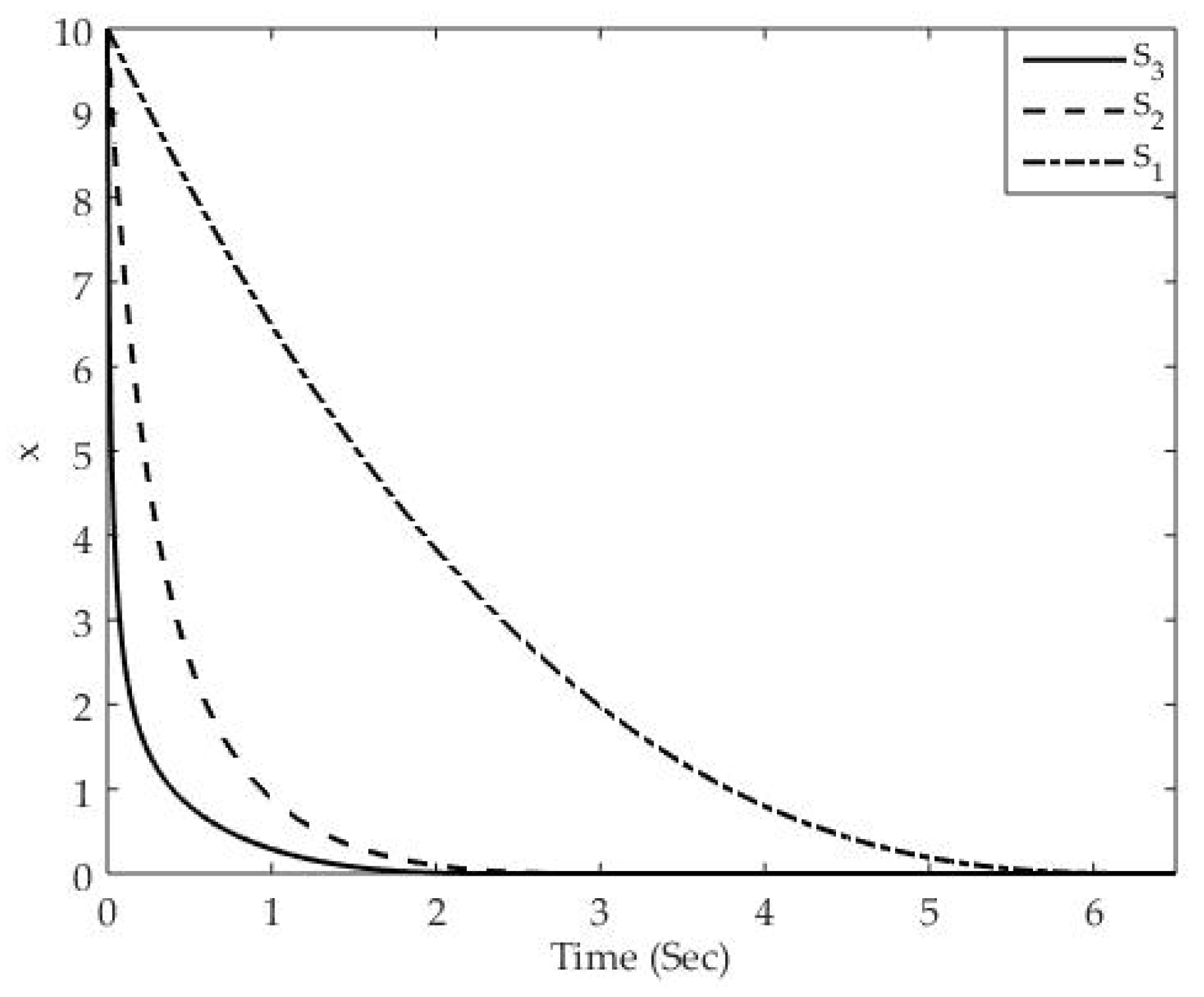
There is a convergence performance comparison between TSM, FTSM, and the improved NFTSM. The following sliding modes are considered:
S 1 = x ˙ + x 3 5 = 0 , S 2 = x ˙ + x 3 5 + x 5 3 = 0 , S 3 = x + ( x + x 3 ) 5 3 + x ˙ 5 3 = 0
with the initial value x ( 0 ) = 10 . The corresponding response curves are given by Figure 5. It can be seen that the improved NFTSM ( S 3 ) has a faster convergence rate than FTSM ( S 2 ) and TSM ( S 1 ).

5. Controller Design of DC-DC Converter

Now, consider the dynamical system (45), according to the scheme of NFTSM, the switching surface is defined as follows:
S 3 = x + k 1 ( x + k 3 x b ) a + k 2 x ˙ c
For the proposed converter with a single switch, a general control law satisfying the hitting condition can be plotted as:
u = 1 = O N , S 3 > 0 0 = O F F , S 3 < 0
To guarantee that the system state stays within the vicinity of the sliding surface, the existence condition derived from Lyapunov’s direct method must be obeyed:
lim S 0 S 3 S ˙ 3 < 0 = S 3 0 + , S ˙ 3 < 0 S 3 0 , S ˙ 3 > 0
where S ˙ 3 is the time derivative of S 3 , and is shown as follows:
S ˙ 3 = 1 + k 1 a e + k 3 e b a 1 1 + k 3 b e b 1 e 2 k 2 c e 2 c 1 e 2 R C o + V i n + V C 1 V o / 2 L 2 C o 1 u
Substituting (56) into (55) gives the following existence condition:
0 < k 2 c e 2 c R C o 1 + k 1 a e + k 3 e b a 1 1 + k 3 b e b 1 e 2 < k 2 b c e 2 c 1 V i n + V C 1 V o / 2 L 2 C o
every coefficient must be satisfied by (57), considering the minimum of the load.
To overcome a variable switching frequency of this system suffering external disturbance, an equivalent sliding mode control with constant operation frequency is adopted.
Equating
S ˙ 3 = 0
yields the equivalent control input:
u e q = 1 + L 2 C o 1 + k 1 a e + k 3 e b a 1 1 + k 3 b e b 1 i C o C o 2 c + i C o R C O 2 k 2 c ( V i n + V C 1 V o / 2 )
To improve the transient response, an exponential reaching law is chosen, and can be expressed as:
S ˙ 3 = k 4 S 3 k 5 s i g n ( S 3 )
where k 4 , k 5 are positive parameters.
When (60) is solved for u, the control input can be obtained as:
u = 1 + L 2 C o 1 + k 1 a e + k 3 e b a 1 1 + k 3 b e b 1 i C o C o 2 c + i C o R C O 2 + k 4 S 3 + k 5 sgn S 3 k 2 c ( V i n + V C 1 V o / 2 )
Finally, the control input u and ramp signal V r a m p = 1 with a constant frequency were fed into a pulse-width modulator to produce the practical control input. Thanks to u, the system converged quickly to an equilibrium point within a finite time. It should be noted that no singularity exists during the whole process, owing to 0 < c < 2 .
Theorem 1.
For the system (45), when the control input is chosen as (61), the system trajectory will then converge quickly to a steady state within a finite time.
Proof of Theorem 1.
Consider the Lyapunov function candidate as:
V = 1 2 S 2
whose time derivative is
V ˙ = S S ˙ = k 2 k 4 c e ˙ 1 c 1 S 2 k 2 k 5 c e ˙ 1 c 1 S
It can be seen that when e ˙ 1 0 , V ˙ 0 , the system state will slide to the sliding mode S = 0 within a finite time. When e ˙ 1 = 0 , by substituting (61) into the second equation of (45), one can obtain:
e ˙ 2 = 1 + k 1 a e + k 3 e b a 1 1 + k 3 b e b 1 k 2 c e ˙ 1 2 c k 4 S k 5 sgn S
Equation (64) can be rewritten as:
e ˙ 2 = k 4 S k 5 sgn S
This equation indicates that e ˙ 2 < k 5 for S > 0 and e ˙ 2 > k 5 for S < 0 . Therefore, the system trajectory will continue moving to an equilibrium point instead of staying on the state of e 1 0 and e 2 = 0 . Moreover, it can be assumed that there exists a vicinity of e 2 = 0 , e 2 δ , ( δ is a positive constant) and satisfying e ˙ 2 < k 5 for S > 0 and e ˙ 2 > k 5 for S < 0 , respectively. Therefore, the crossing of trajectories between two boundaries of e 2 δ is achieved in a finite time, and the trajectory from the region e 2 δ reach the boundaries in finite time too. It can be summarized that the system controlled by (61) can converge to S = 0 from any initial state within a finite time. This completes the proof. □

6. Experimental Results

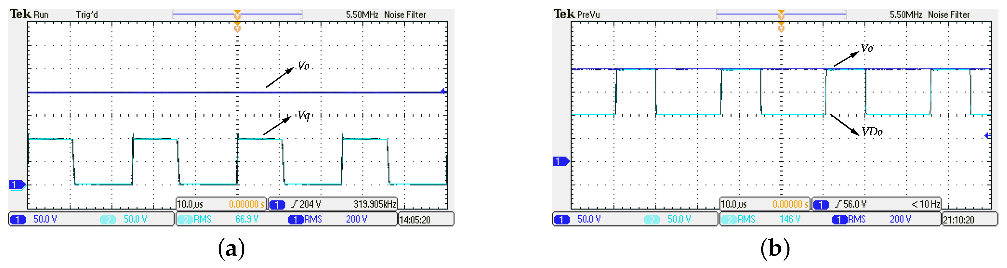
To illustrate the effectiveness of the previous theoretical analysis, a laboratory prototype of the proposed converter was built and experimented. The related parameters of this system are shown in Table 2.
Figure 6 shows the voltage waveforms across the switch and output diode ( D o ), respectively when the output voltage is at 200 V. From (a), it shows that the voltage of the switch equals to 100 V at the “OFF” state, with a small voltage spike about 10 V at the moment when the switch turned off. The subgraph (b) shows that the anode voltage of the output diode ( D o ) to the ground reaches 100 V at the reversed state when the cathode voltage is at 200 V with no voltage spike. One can see that the voltage stress of the output diode arrives at 100 V equalling to half of the output voltage too. Therefore, the voltage stresses of the output diode and switch have been alleviated.
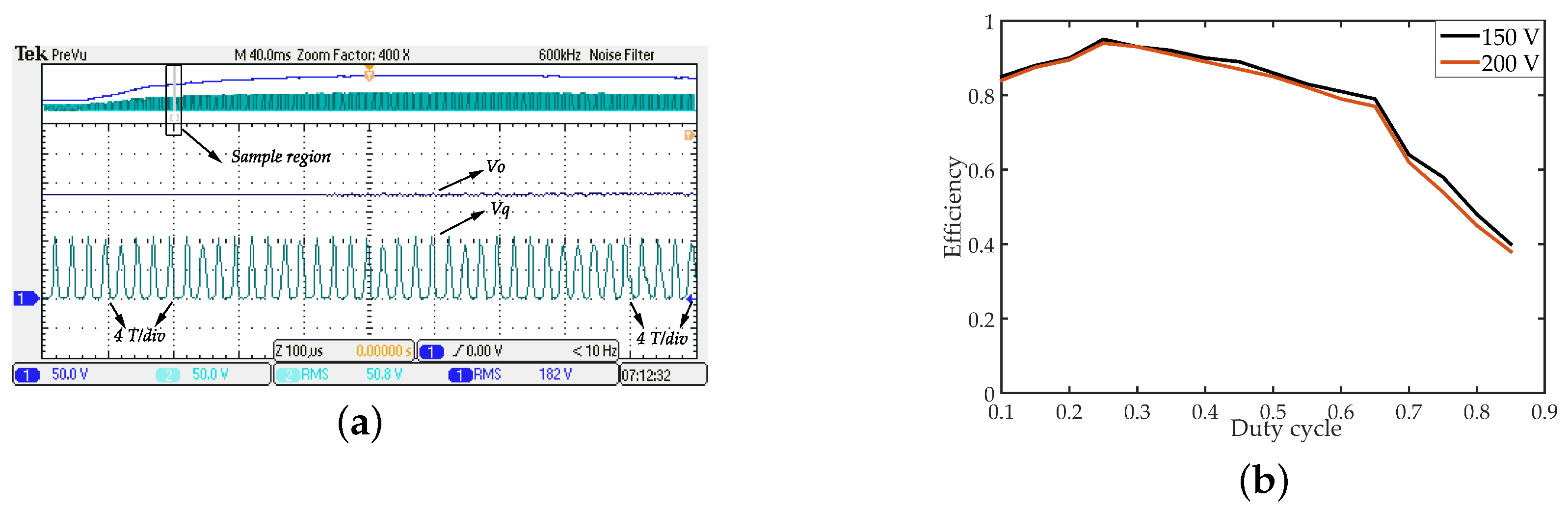
Figure 7a indicates that the switching waveform maintains about four periods in a grid that represents 100 μ s against a variational output voltage. One can see that the equivalent control (u) keeps the switching period constant, at about 25 μ s.
The efficiency versus a wide range of duty cycle and output voltage is plotted in Figure 7b. It shows that the peak efficiency reaches 95% at D = 0.25 , V o = 150 V. The efficiency reduces with the increase of the duty cycle, due to an increasing duty cycle accompanied by a more severe conduction loss of the switch and reverse loss of diodes. In addition, the efficiency, at a 150 V output voltage, only has a small advantage than when the output voltage is 200 V, meaning that the output voltage also has a slight impact on the efficiency. This is because the improved output voltage aggravates the heat loss of inductors and capacitors.
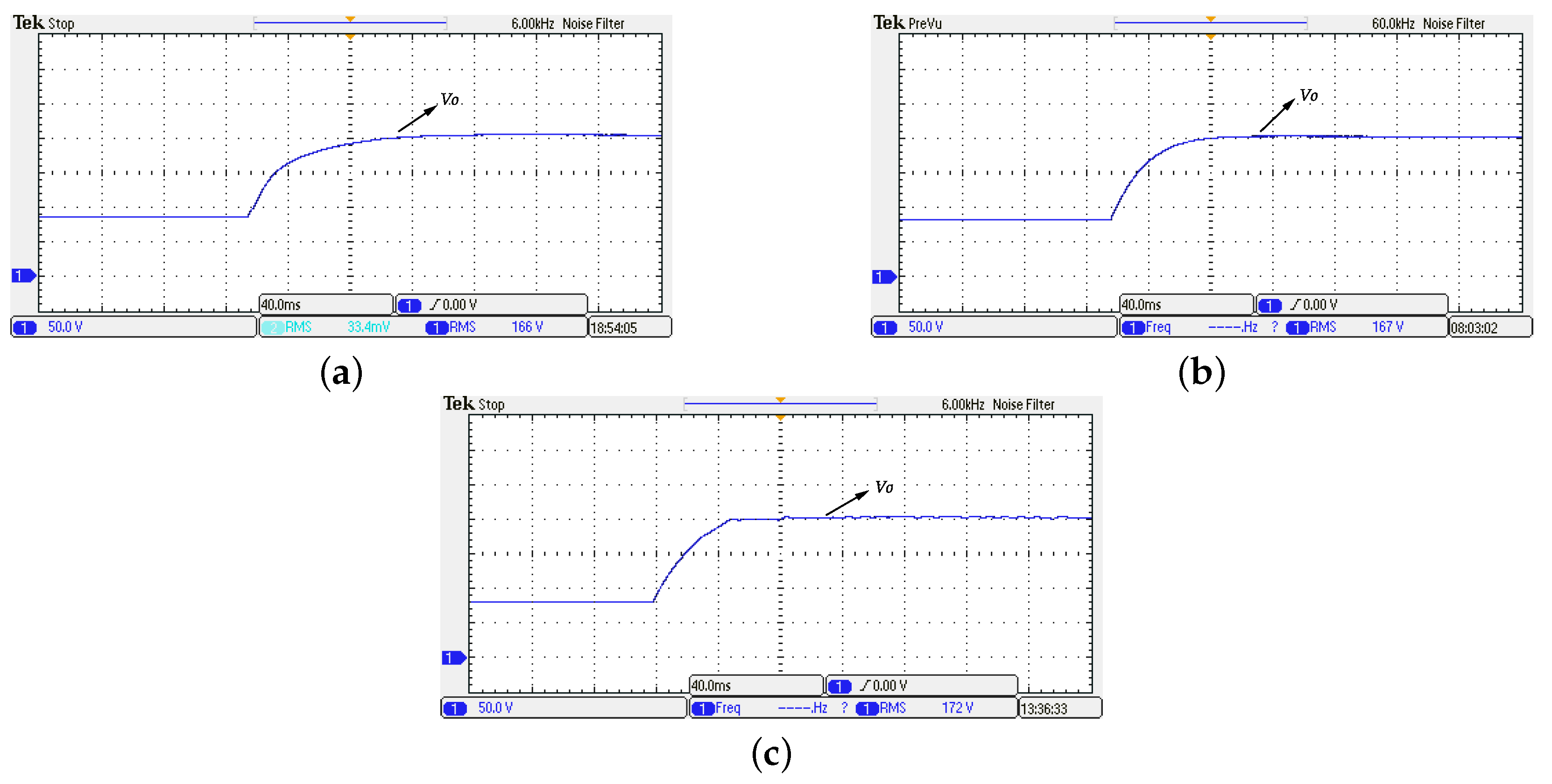
An experiment was also carried out for the performance analysis of the proposed NFTSM controller. The result is given in Figure 8, Figure 9 and Figure 10. The startup transient response is shown in Figure 8, the output voltage against input voltage variation plots in Figure 9, and the output voltage versus load disturbance is illustrated in Figure 10, respectively.
Figure 8 shows the transient response of the output voltage. Figure 8c, one can seen that the output voltage controlled by the proposed controller can track the reference value (200 V) with no overshoot, and has a settling time about 48 ms. Figure 8a, the system controlled by the TSM controller ( S 1 ) takes 104 ms to reach the reference value (200 V), and the system controlled by the FTSM controller ( S 2 ) has a settling time of 64 ms in Figure 8b. we can notice that the proposed controller has a 29.4%, 64.8% settling time improvement than FTSM and TSM, respectively, in this system.
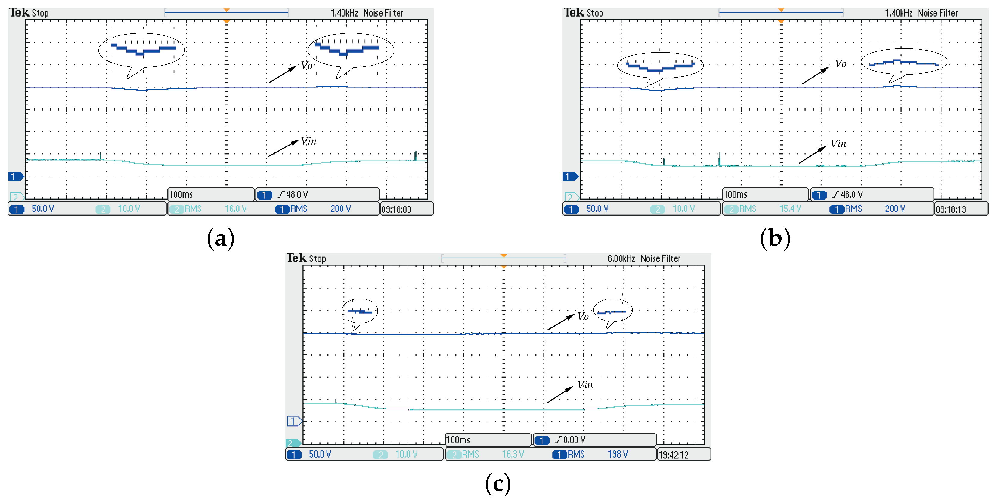
Figure 9 shows the steady output voltage ( V o ) comparison against input voltage disturbance. The input voltage changes from 17 V to 15 V (11.7%) and then returns to 17 V. From the Figure 9c, the output voltage ( V o ) response exhibits no obvious variation. Figure 9a, one can see that the output voltage ( V o ) response controlled by the TSM controller ( S 1 ) takes about 100 ms to recover to the reference value, accompanied by a variation of 10 V (5%). The output voltage ( V o ) response controlled by the FTSM controller ( S 2 ) has a 80 ms recovery time, and a variation of 10 V too in Figure 9b. However, a sharp voltage spike was not visible in the three responses.
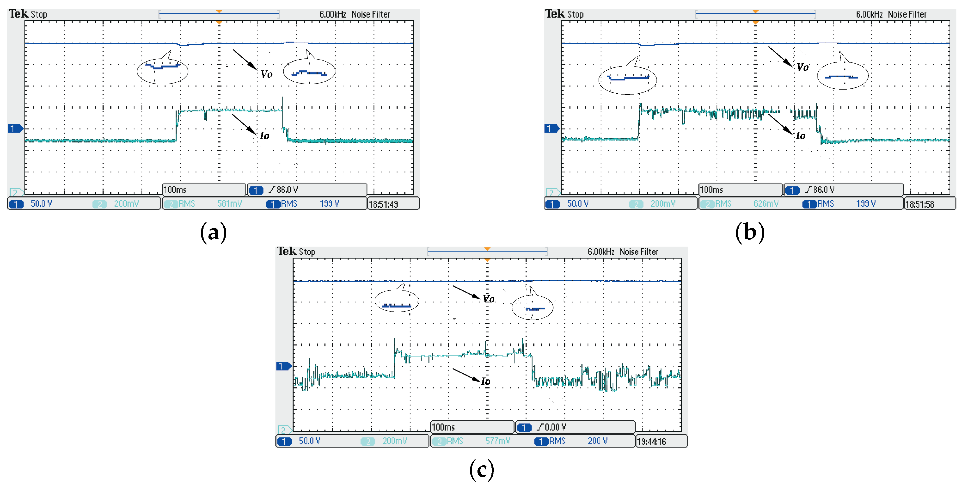
The steady output voltage response versus the output load variation is demonstrated in Figure 10. Here, resistance changes of −150 Ω (−30% variation) were added to a nominal output load of 500 Ω , and then the load returned to 500 Ω . Figure 10c, one can see that the output voltage controlled by the proposed controller almost remains constant at the reference value. Figure 10a, the output voltage controlled by the TSM ( S 1 ) controller has a slight voltage variation of about 8 V, and takes about 60 ms of recovery time after the moment where the load’s resistance has been decreased, and has a settling time of 25 ms with a variation of 8 V after the moment of the load’s resistance turns back. Figure 10b, the output voltage controlled by the FTSM ( S 2 ) controller has 80 ms recovery time with a variation of 5 V after the instant where the load’s resistance is been changed the first time; then, it takes 40 ms to reach the reference signal with a small variation after the moment of the load’s resistance turning back. According to Figure 9 and Figure 10, it can be seen that the proposed NFTSM controller has the strongest robustness amongst the three methods. Based on the above results, it can be noticed that the proposed controller has faster convergence time and greater robustness compared with the TSM ( S 1 ) and FTSM ( S 2 ) controller. Thus, the proposed control scheme is more superior than the TSM and FTSM control strategies for the high step-up converter. In addition, there was no sharp voltage spike in the voltage waveforms of the switch, diodes, and output voltage at different test conditions, meaning that some low-cost elements can be used.

7. Conclusions

A high step-up DC-DC converter based on a single-switch quadratic boost converter and a limited time converge fast terminal sliding mode control strategy was proposed in this paper. Firstly, the operation modes, performance discussion, and key parameter design of the proposed converter were presented. Owing to the voltage multiplier cell, the voltage gain of the proposed converter was highly enhanced; in particular, the peak efficiency reached 95% at an output voltage range of (100 V–200 V). At the mean time, the voltage stresses of the switch and diodes ( D 3 , D 4 , D o ) were decreased to half of the output voltage, and the conversion efficiency was improved. Then, a new finite-time NFTSM scheme was proposed. This can provide a faster convergence rate and stronger robustness than the conventional TSM and FTSM schemes. In particular, the singularity problem does not exist during the whole convergence process. Finally, the proposed controller was applied to the converter to stabilize it and track the reference signal. The experiment demonstrates that the system controlled by the proposed controller can track the reference voltage with a short settling time of about 48 ms and no overshoot. The strong robustness of the proposed controller against input voltage variation and load disturbances was also verified.

Author Contributions

Y.L. designed the NFTSM controller and accomplished the theoretical proof; J.W. designed the topology of the proposed converter, implemented the experiments, and wrote the paper; H.T. designed the circuit and analysed the data.

Acknowledgments

This research was supported by Science and Technology Support Program of Sichuan Province (Grant No. 2016GZ0104).

Conflicts of Interest

The authors declare no conflict of interest. The founding sponsors had no role in the design of the study; in the collection, analyses, or interpretation of data; in the writing of the manuscript, and in the decision to publish the results.

References

  1. Das, M.; Agarwal, V. Novel High-Performance Stand-Alone Solar PV System With High-Gain High-Efficiency DC-DC Converter Power Stages. IEEE Trans. Ind. Appl. 2015, 51, 4718–4728. [Google Scholar] [CrossRef]
  2. Pahlevaninezhad, M.; Das, P.; Drobnik, J.; Jain, P.K.; Bakhshai, A. A novel zvzcs full-bridge dc/dc converter used for electric vehicles. IEEE Trans. Power Electron. 2012, 27, 2752–2769. [Google Scholar] [CrossRef]
  3. Lai, C.M.; Cheng, Y.H.; Hsieh, M.H.; Lin, Y.C. Development of a bidirectional dc/dc converter with dual-battery energy storage for hybrid electric vehicle system. IEEE Trans. Veh. Technol. 2018, 67, 1036–1052. [Google Scholar] [CrossRef]
  4. Mohan, N.; Undeland, T.M.; Robbins, W.P. Power electronics converter, applications and design. Microelectronics 1997, 28, 105–106. [Google Scholar]
  5. Forouzesh, M.; Shen, Y.; Yari, K.; Siwakoti, Y.P.; Blaabjerg, F. High-efficiency high step-up dc-dc converter with dual coupled inductors for grid-connected photovoltaic systems. IEEE Trans. Power Electron. 2018, 33, 5967–5982. [Google Scholar] [CrossRef]
  6. Shi, Y.; Yang, X. Wide Load Range ZVS Three-Level DC–DC Converter: Four Primary Switches, Capacitor Clamped, Two Secondary Switches, and Smaller Output Filter Volume. IEEE Trans. Power Electron. 2016, 28, 3431–3443. [Google Scholar] [CrossRef]
  7. Wong, Y.S.; Chen, J.F.; Liu, K.B.; Hsieh, Y.P. A novel high step-up dc-dc converter with coupled inductor and switched clamp capacitor techniques for photovoltaic systems. Energies 2017, 10. [Google Scholar] [CrossRef]
  8. Wong, Y.S.; Chen, J.F.; Liu, K.B.; Jimichi, T.; Fujita, H.; Akagi, H. A Dynamic Voltage Restorer Equipped With a High-Frequency Isolated DC-DC Converter. IEEE Trans. Ind. Appl. 2011, 47. [Google Scholar] [CrossRef]
  9. Saravanan, S.; Babu, N.R. Design and development of single switch high step-up dc-dc converter. IEEE J. Emerg. Sel. Top. Power Electron. 2018, 6, 855–863. [Google Scholar] [CrossRef]
  10. Wong, Y.S.; Chen, J.F.; Liu, K.B. Realizability conditions and bounds on synthesis of switched-capacitor DC-DC voltage multiplier circuits. IEEE Trans. Circuits Syst. I 1997, 44, 684–691. [Google Scholar] [CrossRef]
  11. Leyva-Ramos, J.; Ortiz-Lopez, M.G.; Diaz-Saldierna, L.H. Switching regulator using a quadratic boost converter for wide DC conversion ratios. IET Power Electron. 2009, 8, 605–613. [Google Scholar] [CrossRef]
  12. Zhang, N.; Sutanto, D.; Muttaqi, K.M.; Zhang, B. High-voltage-gain quadratic boost converter with voltage multiplier. IET Power Electron. 2015, 8, 2511–2519. [Google Scholar] [CrossRef]
  13. Beni, S.H.; Mirtalaei, S.M.M.; Kianpour, A.; Beni, S.A. Design and improvement of a soft switching high step-up boost converter with voltage multiplier. IET Power Electron. 2017, 10, 2163–2169. [Google Scholar] [CrossRef]
  14. López, M.; De Vicuña, L.G.; Castilla, M.; Gayà, P.; López, O. Current distribution control design for paralleled DC/DC converters using sliding-mode control. IEEE Trans. Ind. Electron. 2004, 51, 419–428. [Google Scholar] [CrossRef]
  15. Babazadeh, A.; Maksimovic, D. Hybrid Digital Adaptive Control for Fast Transient Response in Synchronous Buck DC-DC Converters. IEEE Trans. Power Electron. 2009, 24, 2625–2638. [Google Scholar] [CrossRef]
  16. Hsu, C.F.; Lee, T.T.; Wen, Y.W.; Ding, F.S. Intelligent Control for DC-DC Power Converter with Recurrent Fuzzy Neural Network Approach. In Proceedings of the 2006 IEEE International Conference on Fuzzy Systems, Vancouver, BC, Canada, 16–21 July 2006. [Google Scholar] [CrossRef]
  17. Wai, R.; Shih, L. Design of Voltage Tracking Control for DC-DC Boost Converter Via Total Sliding-Mode Technique. IEEE Trans. Ind. Electron. 2011, 58, 2505–2511. [Google Scholar] [CrossRef]
  18. Tan, S.C.; Lai, Y.M.; Chi, K.T. General design issues of sliding-mode controllers in DC-DC converters. IEEE Trans. Ind. Electron. 2008, 55, 1160–1174. [Google Scholar] [CrossRef]
  19. Mohan, N.; Undeland, T.M.; Robbins, W.P. A unified approach to the design of pwm-based sliding-mode voltage controllers for basic dc-dc converters in continuous conduction mode. IEEE Trans. Circuits Syst. 2006, 53, 1816–1827. [Google Scholar] [CrossRef]
  20. He, Y.; Luo, F.L. Sliding-mode control for dc-dc converters with constant switching frequency. IEE Proc. Control Theory Appl. 2006, 53, 37–45. [Google Scholar] [CrossRef]
  21. Wu, Y.Q.; Yu, X.; Man, Z. Terminal sliding mode control design for uncertain dynamic systems. Syst. Control Lett. 1998, 34, 281–288. [Google Scholar] [CrossRef]
  22. Yu, X.; Man, Z. Fast terminal sliding-mode control design for nonlinear dynamical systems. IEEE Trans. Circuits Syst. 2002, 49, 261–264. [Google Scholar] [CrossRef]
  23. Abramowitz, M.; Stegun, I.A. The title of the cited contribution. In Handbook of Mathematical Functions: With Formulas, Graphs, and Mathematical Tables; Publishing House: New York, NY, USA, 1972. [Google Scholar]
  24. Prudente, M.; Pfitscher, L.L.; Emmendoerfer, G.; Romaneli, E.F.; Gules, R. Voltage Multiplier Cells Applied to Non-isolated DC-DC Converters. IEEE Trans. Power Electron. 2008, 49, 871–887. [Google Scholar] [CrossRef]
  25. Feng, Y.; Yu, X.; Man, Z. Non-singular terminal sliding mode control of rigid manipulators. IET Power Electron. 2002, 38. [Google Scholar] [CrossRef]
Figure 1. The equivalent circuit of the proposed converter.
Energies 12 01716 g001
Figure 2. Operation modes: (a) mode 1; (b) mode 2; (c) mode 3; (d) mode 4; (e) mode 5; (f) mode 6.
Energies 12 01716 g002
Figure 3. Key operation waveforms.
Energies 12 01716 g003
Figure 4. Voltage gain comparison of converters.
Energies 12 01716 g004
Figure 5. The comparison of convergence performance between NFTSM, FTSM, and TSM.
Energies 12 01716 g005
Figure 6. The performance of the proposed converter: (a) the voltage wave of the switch (Q); (b) the voltage wave of the output diode ( D o ).
Energies 12 01716 g006
Figure 7. The experiment performance of the proposed converter: (a) the switching frequency against the output voltage variation; (b) the efficiency versus duty cycle and output voltage.
Energies 12 01716 g007
Figure 8. The transient response of the system: (a) controlled by the TSM controller ( S 1 ); (b) controlled by the FTSM controller ( S 2 ); (c) controlled by the proposed NFTSM controller ( S 3 ).
Energies 12 01716 g008
Figure 9. The response of the system versus input voltage variation: (a) controlled by the TSM controller ( S 1 ); (b) controlled by the FTSM controller ( S 2 ); (c) controlled by the proposed NFTSM controller ( S 3 ).
Energies 12 01716 g009
Figure 10. The response of the system against load disturbance: (a) Controlled by the TSM controller ( S 1 ); (b) controlled by the FTSM controller ( S 2 ); (c) controlled by the proposed NFTSM controller ( S 3 ).
Energies 12 01716 g010
Table 1. The voltage stress comparison of key devices.
Key Power DevicesThe Proposed ConverterThe Converter in [9]The Converter in [10]The Boost ConverterThe Quadratic Converter
Q V o / 2 2 V o 3 + D 2 V o 2 + n k + n D k V o V o
D o V o / 2 D V o 2 ( 1 D ) 2 + n D K V o 2 + n k + n D k V o V o
Table 2. Related parameters of this system.
Components L 1 L 2 L r C 1 C r C c C o Rf V i n
value150  μ H200  μ H μ H470  μ F4.7  μ F47  μ F470  μ F500  Ω 40 kHz16 V
Components V o k 1 k 2 k 3 k 4 k 5 abc
value200 V103.4330.1103 5 3 5 3

