Article

A Loss-Free Resistor-Based Versatile Ballast for Discharge Lamps

by
Hugo Valderrama-Blavi
*,
Antonio Leon-Masich
,
Carlos Olalla
and
Àngel Cid-Pastor
Department of Electrical, Electronic, and Automatic Control Engineering (DEEEA), Universitat Rovira i Virgili, 43007 Tarragona, Spain
*
Author to whom correspondence should be addressed.
Energies 2019, 12(7), 1403; https://doi.org/10.3390/en12071403
Submission received: 4 March 2019 / Revised: 5 April 2019 / Accepted: 7 April 2019 / Published: 11 April 2019
(This article belongs to the Special Issue Sliding Mode Control of Power Converters in Renewable Energy Systems)

Abstract

:
This paper presents a versatile ballast for discharge lamps, whose operation is based on the notion of a loss-free resistor (LFR). The ballast consists of two stages: (1) a boost converter operating in continuous conduction mode (CCM) and exhibiting an LFR behavior imposed by sliding-mode control; and (2) a resonant inverter supplying the discharge lamp at high frequencies. Thanks to this mode of operation, the power transferred to the lamp is regulated by the LFR input resistance, allowing successful ignition, warm-up, nominal, and dimming operation of a range of discharge lamps, with no need for complex regulation schemes based on lamp models. The versatility of the ballast has been experimentally proven for both conventional and electrodeless discharge lamps. Tests include induction electrodeless fluorescent (IEFL), high-pressure sodium (HPS) vapor, and metal-halide lamps.

1. Introduction

Lighting from electricity accounts for approximately 15–19% of global energy consumption and over five percent of worldwide greenhouse gas (GHG) emissions. It has been estimated that replacing all inefficient on-grid lighting would result in 939 TWh of electricity savings annually, which correspond to approximately 490 million tons of CO2 [1,2]. For that reason, efficient lighting sources, such as light-emitting diodes (LEDs) and discharge lamps, are increasingly used as a simple and cheap procedure to reduce the contribution of electricity consumers to global warming [3,4,5,6,7]. In this sense, although LEDs are steadily increasing their rated power and luminous efficacy in terms of lumen/Watt, discharge lamps are still competitive in applications requiring high power and long lifespan. Concretely, for a given discharge lamp type, higher-power bulbs usually have better efficacy than lower-power ones [8]. In contrast, due to the efficiency droop, the situation is normally the opposite in LEDs, making them more suitable for low-power applications [9]. Regarding lifetime, although high-performance LEDs last about 50,000 h, and high-pressure sodium (HPS) or metal-halide (MH) lifespan is between 15,000 and 25,000 h, external coil induction electrodeless fluorescents (IEFLs) can last up to 100,000 h with a very little light output depreciation until the very end of its life.
Many types of discharge lamps are available in the market, differing in the type of gas, filling pressure, operating voltage, color rendering index, or efficiency. One of the main differences among them is the way the electrical energy is transferred to the bulb. Whereas conventional lamps use internal electrodes to transfer the energy to the bulb, the magnetic induction electrodeless lamps use internal or external coils to do so. This coil behaves as the primary winding of a transformer, whereas the discharge operates as the secondary one-turn coil.
Although single-stage solutions exist [10,11,12,13], ballasts for discharge lamps are typically composed of two stages [14]. The first stage is a buck, boost, or buck-boost stage performing power factor correction (PFC) and providing an approximately constant DC-link voltage. The second stage is a full or half-bridge LCC resonant converter driving the lamp.
In this context, power regulation is the subject of many papers because dimming operation can provide about a 50–60% energy saving [7,12,15]. The issue is still open to discussion because discharge lamp systems are expensive, and light-dimming normally requires a more complex circuitry than traditional systems without light regulation. In high-intensity discharge (HID) lamps, current mode control is the most extended technique [10], such that power control can be realized by analog multiplication of voltages and currents within the lamp. Also, other techniques have been used, such as controlling the resonant tank input current [11]. Regarding IEFLs, J. Tae-Kun et al. [16] present a comparison between two power control methods: the variable switching frequency control and the variable DC-link voltage control method, to conclude that the latter is more suitable for linear dimming operation of the lamp. Later, several authors presented power conversion topologies dedicated to regulating the light in the IEFL [17,18,19,20] with the aim to compare performance and efficiency in the converters. In all these cases dimming control is achieved by adjusting the DC-link voltage. The common characteristic in all the previous works is the necessity of exactly understanding the lamp behavior, and its electrical characteristics at different power ratings [21] to achieve power regulation. However, precise lamp modelling also implies that each ballast is designed for a given lamp type, which results in the opposite concept of a versatile design.
In this paper, a novel approach for power control in electronic ballasts is proposed. The approach is based on a conventional two-stage ballast: besides of performing PFC, the first stage has the characteristics of a loss-free resistor (LFR), whereas the second stage simply converts the DC input power into the required AC waveforms at the desired frequency. The LFR is a POPI device [22,23] whose output port is a power source which delivers to the load the power absorbed by the emulated input resistance, no matter what type of lamp is connected at the output. Consequently, the power injected in the lamp can be accurately regulated with a simple controller and with no stability issues, no matter what impedance the lamp connected at the output presents. In other words, the proposed ballast does not require lamp modelling. The second stage operates as an inverter, whose switching frequency can be selected depending on the requirements of the lamp. In this sense, the paper also presents a method to design a resonant tank that is compatible with several discharge lamp types. Thanks to these features, the only expected limits on the ballast versatility is the rating of the components used in the power stages. The proposed approach results in three advantageous characteristics. First, the proposed ballast is extremely versatile. Secondly, stability is ensured irrespective of the frequency response of the lamp. Finally, light-dimming control can be achieved easily by adjusting the LFR input power.
The proposed approach could be applied to any discharge lamp. In the paper, we have demonstrated the ballast with a prototype that can drive some of the most common types. Specifically, the paper shows results for an IEFL, a HPS vapor lamp, and two MH lamps.
The remaining part of this article is organized as follows: the proposed ballast and the lamp start-up procedure are described in Section 2. An appropriate sliding-mode control is applied to the boost converter to impose an LFR behavior in Section 3. The effect of different lamp models in the resonant inverter design and the ballast stability is analyzed in Section 4. Experimental results demonstrating the feasibility of the proposed ballast are shown in Section 5. The conclusions and future research are presented in Section 6.

2. Proposed LFR-Based Ballast

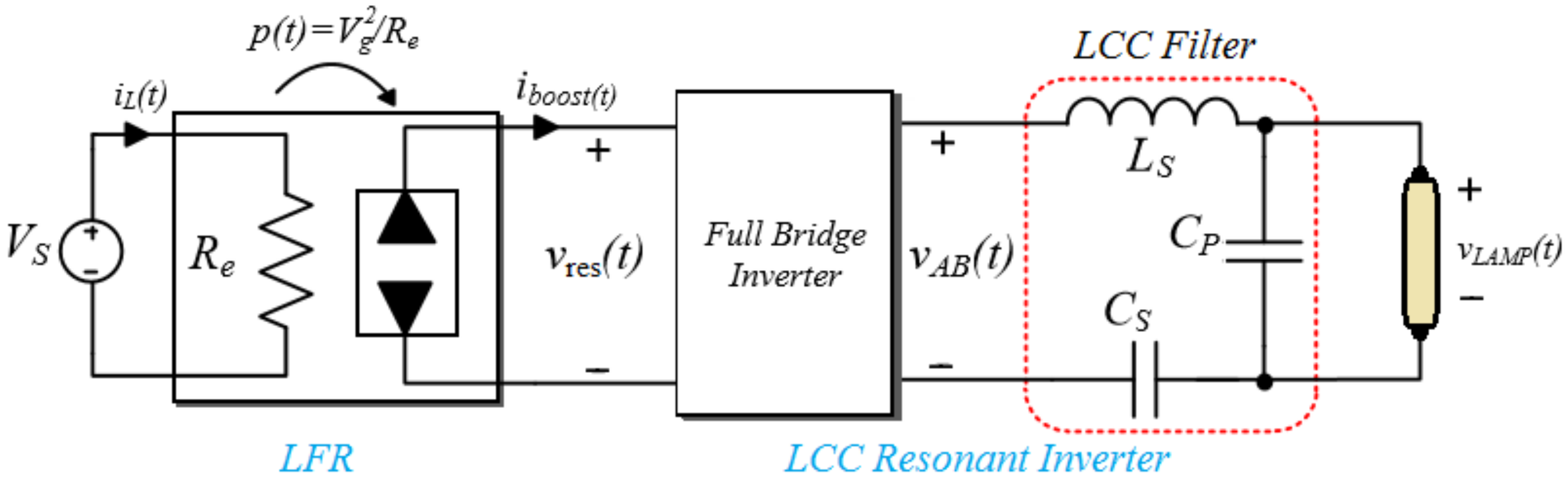
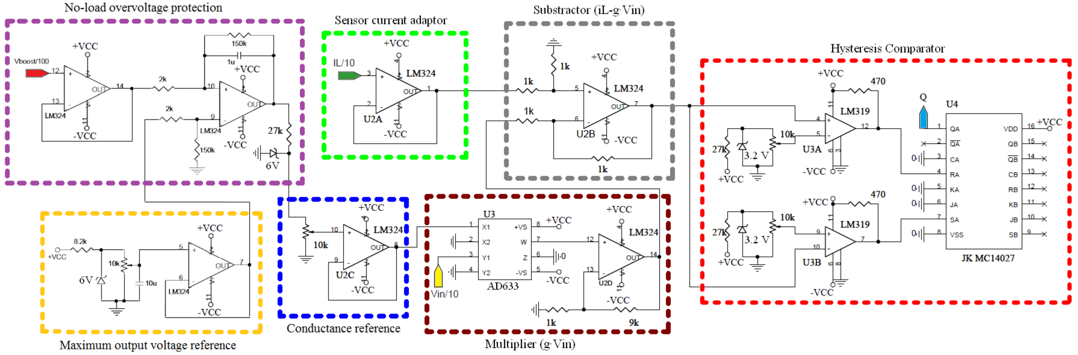
The operation of the proposed ballast in steady-state combines the features of its two stages, i.e., LFR and resonant inverter depicted in Figure 1. The LFR stage assures the lamp supply with both constant and adjustable power to regulate the luminosity and protect the lamp. As an advantage, the LFR behavior precludes the instabilities caused by the negative incremental impedance of many discharge lamps.
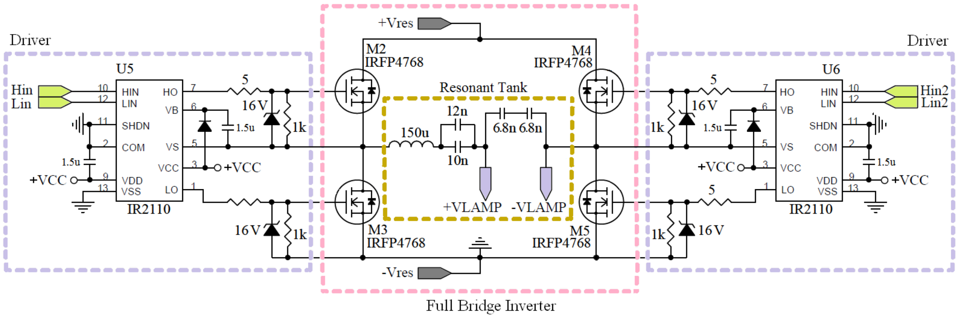
The resonant inverter stage is required to supply the lamps in AC at high frequency (90–250 kHz). AC supply is needed to avoid electrode wear in voltage driven discharge lamps, and to make the IEFL coils behave like a transformer.
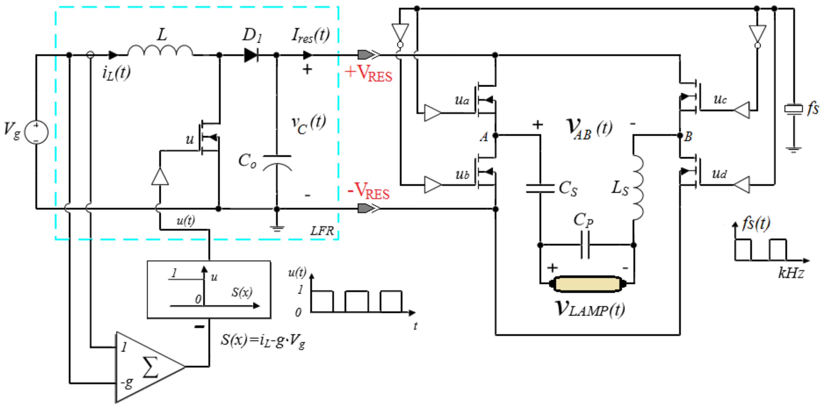
Figure 2 depicts the schematic of the proposed ballast. The LFR is implemented by an appropriate sliding-mode control in a boost converter supplied by low-voltage DC source (such as a car battery) ranging from 12 V to 15 V. The figure shows a DC input, but the proposed approach can also be applied in the case that V g is the AC input from a rectifier. Also in the figure, a boost converter is considered, but other topologies (such as the buck-boost, flyback or forward) could be employed if the ballast is supplied from the grid.
The regulation of the lamp requires very different modes of operation: start-up, warm-up, nominal output, and dimming. Thanks to the LFR behavior, the ballast operates as a power source regardless of the mode, and control is straightforward.

2.1. Lamp Start-Up

In electroded lamps, many factors influence the peak voltage required to start the lamp. Among them the distance between electrodes, the gas type and pressure, and in the case of MH lamps, the existence or nonexistence of a third electrode to reduce the strike voltage. When an electroded lamp is OFF, its impedance is an open circuit, and the ballast is unloaded. In pulse-start lamps, a high peak voltage is required, ranging from 1.5 kV up to 30 kV (hot re-strike). In probe-start lamps, due to the third electrode, start voltages are in the range of 500 V or less.
External coil IEFLs are slightly different. When a IEFL lamp is OFF, the lamp input impedance is purely reactive, and equal to the external coil inductance. Thus, the lamp behaves like an unloaded transformer.
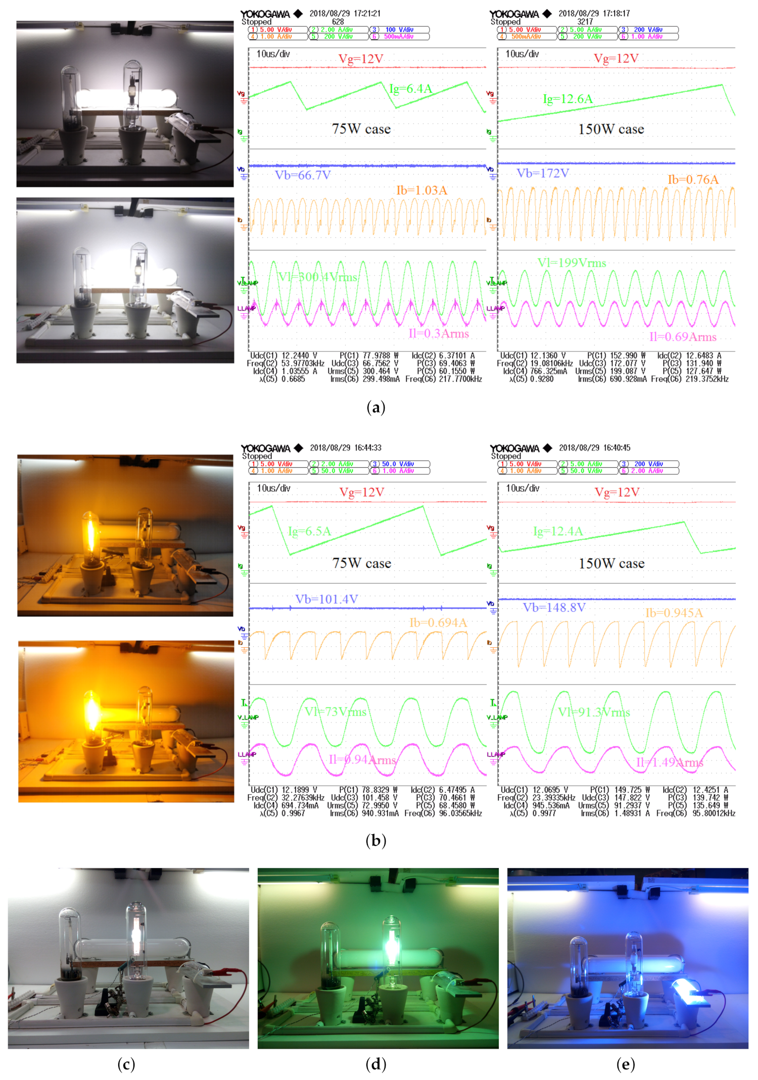
In the proposed ballast, the first and the second stages contribute to reach the required voltage to start the lamps, directly inducing the required electric field inside the bulb with the electrodes, or through Faraday’s Law in the external coil IEFL. A single resonant tank is used for all lamps, and the inverter frequency is adjusted to operate the tank a a frequency that provides the required voltage gain from the second stage, which in our case is 224 kHz. As the boost converter is unloaded, its output voltage increases continuously until the lamp starts-up, or the boost output reaches the maximum voltage allowed.

2.2. Lamp Warm-Up

Immediately after the start-up, the lamp voltage drops, and warm-up begins. During this process light intensity increases and, in some lamps, color changes are produced. The voltage increases slowly while the current decreases at similar rate, until the steady-state is reached at the warm-up end. It is important to remark that, although the lamp impedance changes during warm-up, the supplied power is controlled by the LFR stage, so damaging the lamp is precluded. In high-pressure devices like metal-halide (MH) and sodium vapor (HPS) lamps, warm-up can last up to 10 min. In contrast, the steady-state luminous flux of IEFLs is reached in few seconds.
In this period, the lamp impedance is no longer an open circuit, and the gain peak of the resonant inverter decreases. However, the impedances of electroded lamps are quite lower than those of IEFL lamps for the same power, and the resonant inverter gain reduction is less severe with IEFL lamps. In the proposed ballast, this gain reduction is automatically compensated by an increment of the LFR stage gain, but as more severe be the resonant gain reduction, more important will be the increase of the LFR gain, and higher will be the component stress in the boost stage, affecting the global ballast efficiency. To avoid a significant gain increase of the LFR stage, the inverter frequency is reduced from 224 kHz to 90 kHz, when the ballast is driving an electroded lamp. This frequency reduction assures at least, a minimum gain of 0 dB for the resonant inverter, thus limiting the gain increase of the LFR stage. The inverter frequency change is not applied with IEFL lamps because they cannot operate below 150 kHz, and the resonant gain reduction is quite less severe.

2.3. Nominal Operating Point and Dimming

After warm-up, the lamp impedance is approximately constant, lamp voltage and current reach their steady state values, and the ballast continues to deliver constant power. If dimming is required, the LFR stage can reduce the power transferred to the lamp, adjusting the LFR input conductance, and dimming takes place independently of the lamp impedance.

3. Sliding-Mode Dynamics of the First Power Stage

This section shows how the LFR can be realized with a sliding-mode controller. A small-signal model is derived, and its stability is proven.
The LFR behavior of the first stage in Figure 2 is achieved by a sliding-mode control loop that makes the boost converter input current proportional to the input voltage. Specifically, the switching surface in (1) forces the input current to track a slow reference k ( t ) proportional to the ballast input voltage v g . Therefore, the lamp active power P a c is indirectly regulated by controlling the converter input power P i n through the adjustment of either the LFR input resistance R e or the LFR input conductance g,
s ( x ) = i L ( t ) k ( t ) , where k ( t ) = g · v g ( t )
g = 1 R e
p i n = g · v g 2 p a c
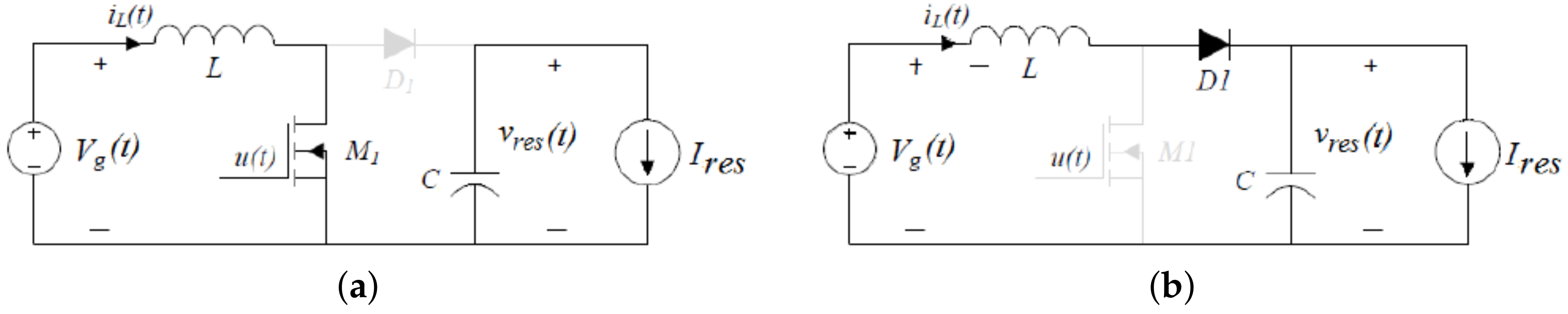
Assuming that the boost converter operates in continuous conduction mode (CCM), only two topological changes occur in a period, as shown in Figure 3. Each converter topology can be represented by means of two linear vector differential Equation (4), where the corresponding state vector is given in (5).
x ˙ ( t ) = A 1 x ( t ) + B 1 , for u = 1 ( ON   State ) x ˙ ( t ) = A 2 x ( t ) + B 2 , for u = 0 ( OFF   State )
x ˙ ( t ) = [ i L , v r e s ] T
Matrices A 1 , A 2 , B 1 and B 2 are given in (6), where, I r e s ( t ) represents the current delivered by the boost-based LFR to the resonant inverter stage.
A 1 = 0 0 0 0 , A 2 = 0 1 L 1 C 0 , B 1 = B 2 = v g ( t ) L i r e s C .
The converter dynamics can be described using the bilinear Equation (7), where A = A 2 , B = A 1 A 2 , δ = B 2 and γ = B 1 B 2 .
x ˙ ( t ) = A · x ( t ) + δ + B · x ( t ) + γ
From (6) and (7) we obtain
d i L ( t ) d t = u 1 L · v r e s ( t ) + v g ( t ) L d v r e s ( t ) d t = 1 u C · i L ( t ) i r e s ( t ) C
If the invariance conditions [24] s ( x ) = 0 and d s ( x ) / d t = 0 are applied in (1), the equivalent control u e q ( t ) can be derived. The equivalent control u e q ( t ) is bounded by the maximum and minimum values of u ( t ) : 0 < u e q ( t ) < 1 . In such case, a switching law of the type
u ( t ) = 0 if s ( x ) > 0 u ( t ) = 1 if s ( x ) < 0
induces a sliding regime on the switching surface, ensuring the sliding-mode existence because
s ( x ) d s ( x ) d t < 0 .
The dynamics are then derived as follows. First, the equilibrium point is found assuming constant values of input voltage v g = V g and LFR input conductance g = G in the control loop. Second, the influence of the time-varying components of the mentioned input variables is analyzed as linearized low-frequency signals superposed on their corresponding values V g and G. Considering constant values for V g and G leads to the equivalent control u e q , ideal sliding dynamics, and equilibrium point X = [ I L , V r e s ] T given in (11)–(13) respectively.
u e q ( t ) = 1 V g v r e s
i L ( t ) = G · V g d v r e s ( t ) d t = G · V g C ( 1 u e q ) i r e s ( t ) C
X = G · V g , V g 2 · G I r e s T
Assuming now that k ( t ) is time-varying, the corresponding equivalent control, and ideal dynamics are given by (14) and (15) respectively
u e q ( t ) = 1 v g ( t ) v r e s ( t ) + L g ( t ) v r e s ( t ) · d v g ( t ) d t + L v g ( t ) v r e s ( t ) · d g ( t ) d t
i L ( t ) = k ( t ) = g ( t ) · v g ( t ) d v r e s ( t ) d t = g ( t ) v g 2 ( t ) C v r e s ( t ) L g 2 ( t ) v g ( t ) C v r e s ( t ) d v g ( t ) d t + g ( t ) v g 2 ( t ) C v r e s ( t ) d g ( t ) d t i r e s ( t ) C
Variables can be expressed as (16), as a sum of its DC component and a small-signal term denoted with a hat sign:
g ( t ) = G + g ^ ( t ) , v g ( t ) = V g + v ^ g ( t ) , i L ( t ) = I L + i ^ L ( t ) , v r e s ( t ) = V r e s + v ^ r e s ( t ) ,
Linearizing the differential equation of the output capacitor (15) around the equilibrium point X = [ I L , V r e s ] T leads to the following expression
f ( x ) = d v ^ r e s ( t ) d t a · g ^ ( t ) + b · d g ^ ( t ) d t + c · v ^ g ( t ) + d · d v ^ g ( t ) d t + e · v ^ r e s ( t ) + f · i ^ r e s ( t )
where coefficients a, b, c, d, e, and f are as follows
a = f ( x ) g ( t ) x = X = I r e s C · G , b = f ( x ) a ( t ) a ( t ) = d g ( t ) d t , x = X = L · I r e s C , c = f ( x ) v g ( t ) x = X = 2 I r e s C · V g , d = f ( x ) b ( t ) b ( t ) = d v s ( t ) d t , x = X = L · I r e s · G C · V g , e = f ( x ) v r e s ( t ) x = X = I r e s 2 C · V s 2 · G , f = f ( x ) i r e s ( t ) x = X = 1 C ,
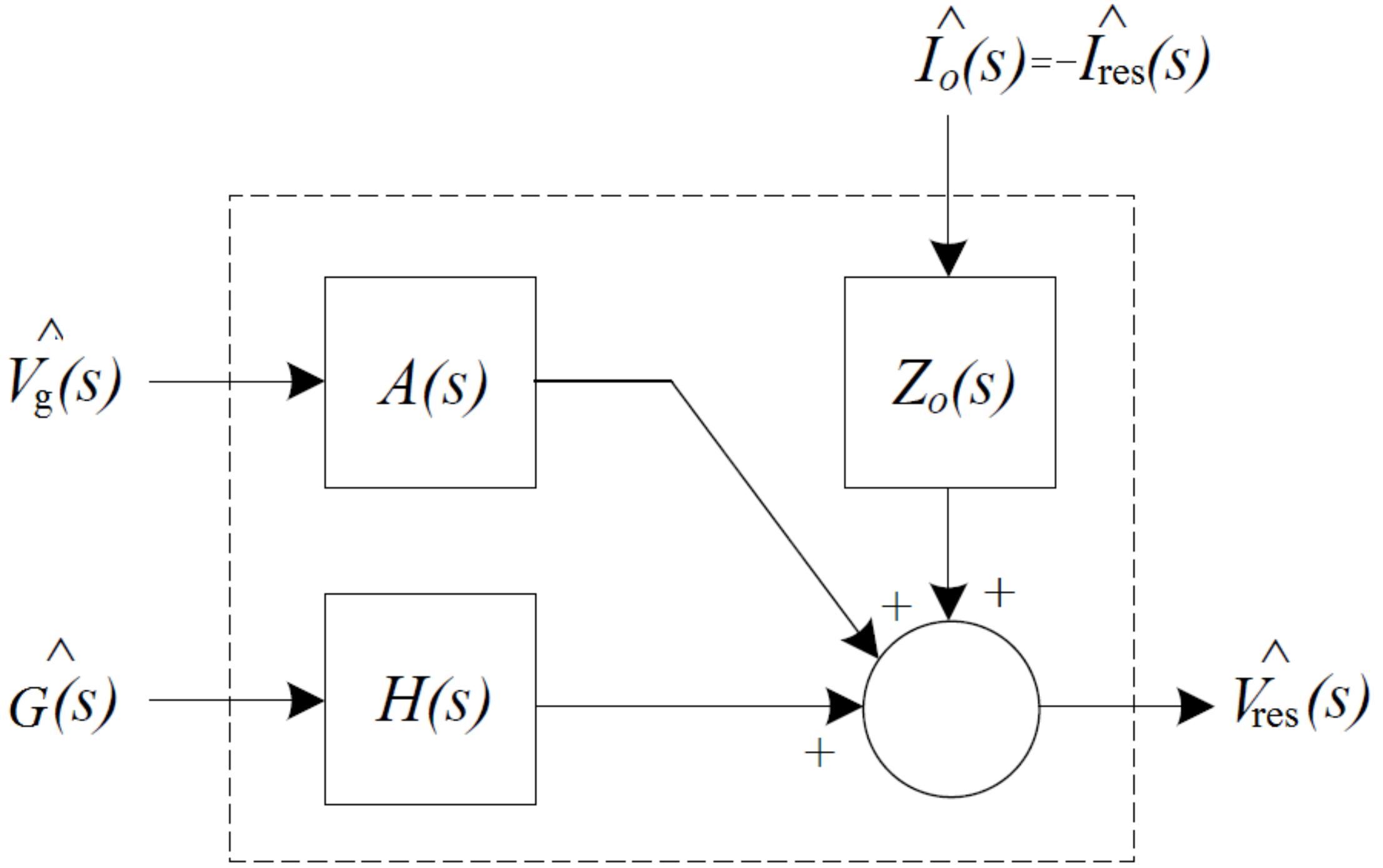
Figure 4 shows the block diagram of the boost converter-based LFR small-signal model. The transfer functions of the block diagram are as follows
H ( s ) = v ^ r e s ( s ) g ^ ( s ) = a + s · b s e = L I r e s C s 1 / ( L G ) s + I r e s 2 / ( C V g 2 G )
A ( s ) = v ^ r e s ( s ) v ^ g ( s ) = c + s · d s e = L I r e s G C V g s 2 / ( L G ) s + I r e s 2 / ( C V g 2 G )
Z o ( s ) = v ^ r e s ( s ) i ^ o ( s ) = v ^ r e s ( s ) i ^ r e s ( s ) = 1 / C s + I r e s 2 / ( C V g 2 G )
Considering that I r e s 2 V g 2 G = 1 Z D C ( P ) , it can be seen that the control to output transfer function H ( s ) given above is stable, because the following condition is always satisfied
I r e s 2 C V g 2 G = I r e s 2 C P i n 1 C Z D C ( P ) > 0

4. Design of the Resonant Tank and System Stability

In the literature there are some works analyzing the L s C s C p resonant filters of electronic ballasts supplying IEFL lamps with dimming operation [16]. Nonetheless, most of these papers do not consider the lamp model, except for [21] where a precise IEFL equivalent model was introduced.
In fact, the resonant converter cannot be analyzed in a classical way, i.e., when the load is a resistor, because its behavior depends on the nonlinear nature of the lamp. Consequently, the input-output voltage transfer function H T ( P , s ) of the converter will depend on the lamp impedance Z l a m p ( P , s ) , which, in turn, is also function of the power P handled by the lamp.
H T ( P , s ) = v ^ l a m p ( s ) v ^ A B ( s ) = Z l a m p ( P , s ) C p s Z l a m p ( P , s ) + 1 C p s 1 Z l a m p ( P , s ) C p s Z l a m p ( P , s ) + 1 C p s 1 + 1 C s s + L s s
In the design of the proposed ballast, two lamp models are used: (a) a general first-order model with a right half-plane zero and a stable pole, and (b) the IEFL model introduced in [
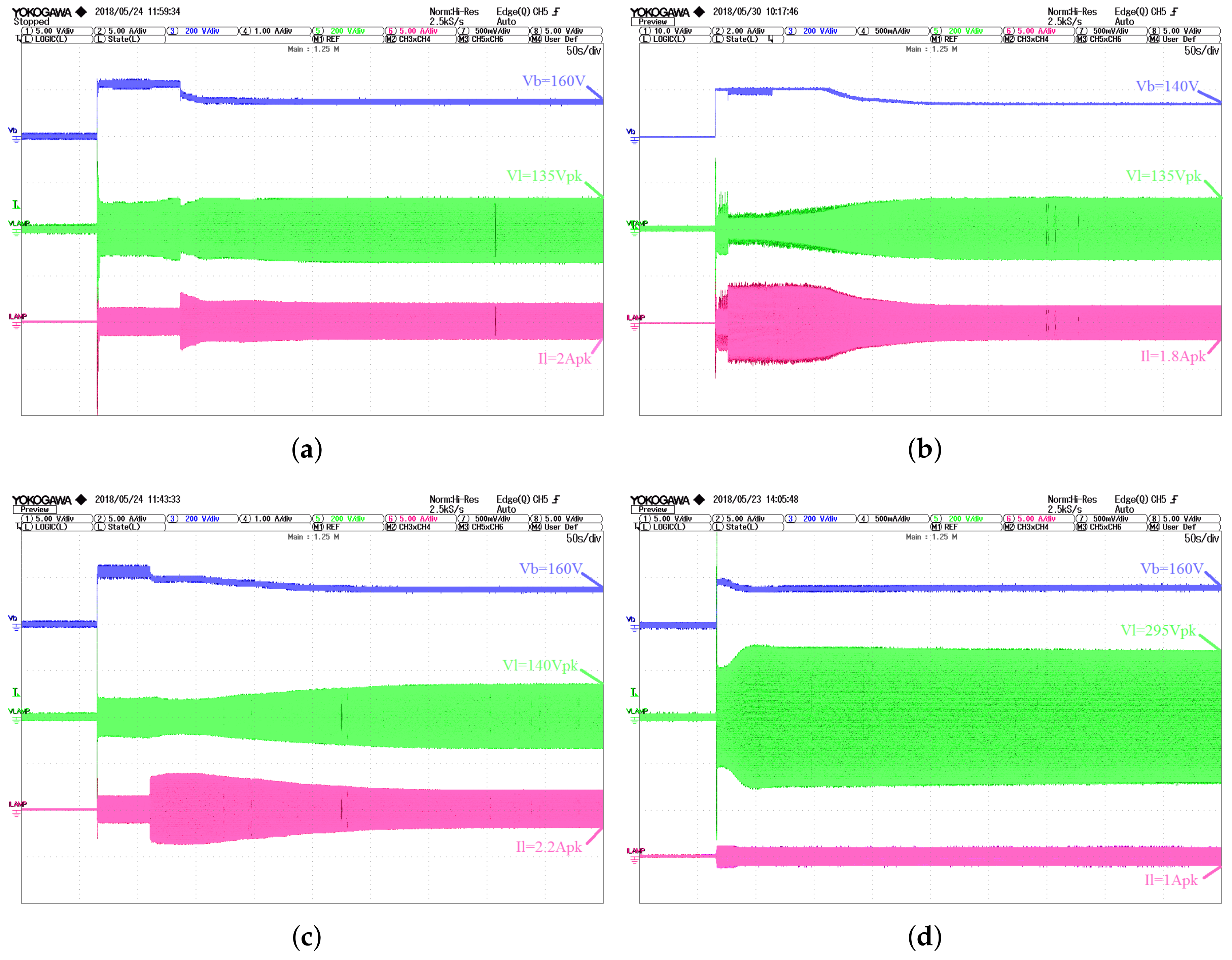
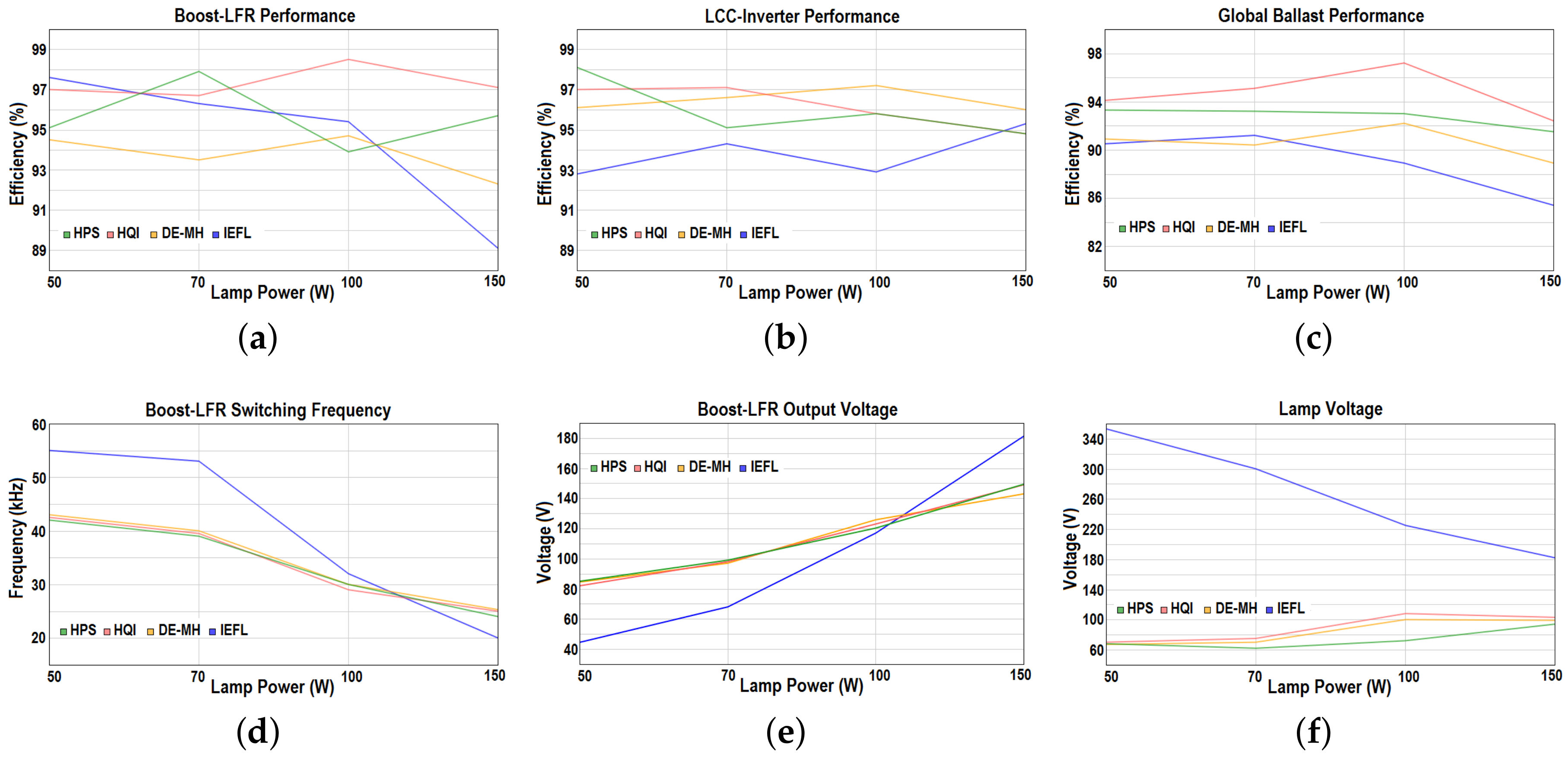
21]. Four lamps have been tested in this paper: a 150 W IEFL from Osram, a 150 W HPS vapor lamp from Sylvania, and two 250 W probe-start MH lamps, from Osram and I-Quarium, respectively. The latter three lamps have internal electrodes and can be described with the first-order model.

4.1. First-Order Lamp Model

All lamps with negative incremental resistance can be described with this model. The impedance parameters are the equivalent DC resistance R L , a real half-plane pole p L , a right-plane zero z L , and a negative resistance λ n
Z H P S M H ( P , s ) = R L ( P ) s + z L s + p L , λ n = R L ( P ) z L p L < 0
The zero is located between 10 and 103 rad/s, and the pole between 100 and 104 rad/s. In reference [25] the parameters of an specific HPS lamp with z L = −3141.5 rad/s and p L = 18.8 rad/s are given, whereas in reference [26], similar parameters for a 150 W MH lamp with z L = −1850 rad/s and p L = 10,690 rad/s can be found. This illustrates the great variability in the location of p L and z L . The ballast operation with HPS and MH lamps is simulated using the values of [25,26] and the real resonant tank values ( L s = 150 μH, C s = 22 nF, and C p = 3.3 nF) of the ballast prototype. The corresponding results are given in Table 1, where Z D C ( P ) = V r e s I r e s .

4.2. IEFL Lamp Model

The IEFL model proposed here is directly derived from the model presented in [21] but has been improved by considering the saturation of the IEFL transformer core. As a result, the parameter L c (which was constant in [21]) is now power dependent. The remaining model parameters continue to be power dependent as they were in [21]. According to the circuit in Figure 5b, the parameters that can be seen from the transformer primary side are: the core losses R C , the inductance L c , the lamp resistance R L which represents the power transformed into light, and the lamp capacitance C L . Expression (25) models the IEFL lamp impedance. According to the procedure given in [21], the parameters of the model of the 150 W IEFL lamp used in the experiments were obtained. Then, these parameters were used to simulate the behavior of the proposed ballast using, as in the previous case, the resonant tank values ( L s = 150 μH, C s = 22 nF, and C p = 3.3 nF). The results of the simulation are given in Table 2.
Z I E F L ( P , s ) = R C R L L C s R C R L L C C L s 2 + L C ( R C + R L ) s + R L R C

4.3. Design of the Resonant Tank

In the proposed ballast, the LFR behavior controls the power delivered to the lamp and makes it possible to provide light-dimming, if necessary. On the other hand, the resonant inverter stage is required to supply the lamps in AC, but also to increase the ballast voltage gain during the lamp start-up by means of the tank resonant gain peak.
The resonant tank voltage gain G ( P , ω ) , can be found from the inverter transfer function in (23) by G ( P , ω ) = | H T ( P , s ) | s = j ω . Nevertheless, to simplify tank design, a reduced gain function G s ( P , ω ) is used. This function can be easily derived from (23) considering the lamp as a power dependent resistor R L ( P ) . By defining the following normalized parameters,
Q L ( P ) = ω o C P 1 + A R L ( P ) , ω o 2 = 1 L s ( C p | | C s ) , A = C p C s Q S ( P ) = Z S R L ( P ) , Z S = 1 ω s C s , ω s 2 = 1 L s C s
two different expressions are obtained for the resonant tank voltage gain G s ( P ) .
G S ( P , ω ) = 1 ( 1 + A ) 2 1 ω ω o 2 2 + 1 Q L 2 ( P ) ω ω o ω o A ω ( 1 + A ) 2
G S ( P , ω ) = 1 1 ω ω s 2 1 A 2 + Q S 2 ( P ) ω ω s ω s ω 2
where A is the parallel to series capacitance ratio, ω o is the undamped resonant frequency, Q L ( P ) is the loaded quality factor, ω s is the series resonant frequency, Z S is the series characteristic impedance, and Q S ( P ) is the series quality factor.
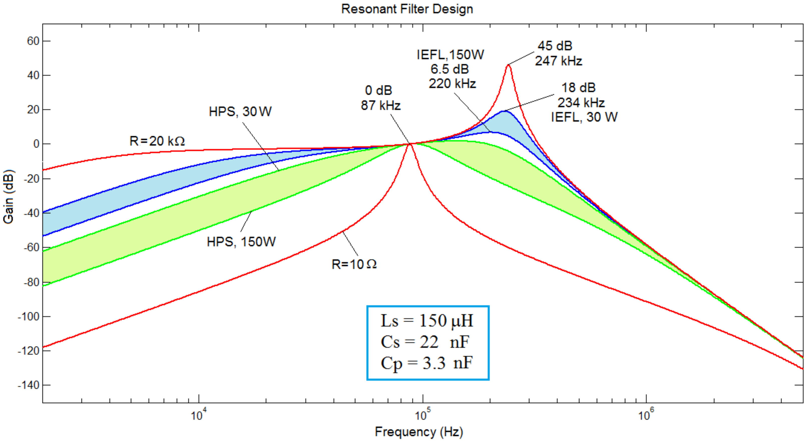
Figure 6 depicts the frequency response of G S ( P , ω ) for different values of lamp power and resistance. There are two different resonant frequencies, i.e., the series resonant frequency ω s , around 90 kHz, and the main resonant frequency ω o , slightly below 250 kHz. The values of the tank components, namely L s = 150 μH, C s = 22 nF, and C p = 3.3 nF are obtained by solving a set of equations as explained below.
The resistive part (active power) of any lamp impedance R L ( P ) is extremely variable with the lamp power, aging, and type of lamp. In fact, in common lamp types, 10 Ω < R L ( P ) < 500 Ω . As the lamp power regulation is ensured by the LFR stage, the inverter stage is only used to provide the appropriate high-frequency AC signal to the lamp, once the lamp is started.
If the lamps are supplied at the series resonant frequency ω s , the series capacitor C s and inductor L s impedances are mutually cancelled, and the resonant inverter has little effect on the lamp regulation because the gain is G S ( P , ω s ) = 0 dB at any load. This choice is the first design constraint, and can be posed as follows
Z L s C s = L s C s s 2 + 1 C s s , Z L s C s ( j ω s ) 0 G S ( ω s ) 0 dB ,
ω s = 1 L s C s = 2 π 87 · 10 3 rad / s .
A notable exception is the IEFL lamps. These lamps include a transformer coil to transfer the energy to the plasma, which is usually designed to work optimally in the range of 200–250 kHz. Besides, they also exhibit a higher input impedance ( 500 Ω < R L ( P ) < 10 k Ω ) than other lamp types, working at higher voltages. As a result, to avoid a boost stage extreme voltage gain, part of the required gain can be supplied by the resonant tank through the second resonance. The frequency of this second resonance is noted ω o , and the voltage gain at this frequency G S ( ω o ) corresponds to the second and third tank design constraints, shown next:
ω o = C s + C p L s C s C p 2 π 245 kHz ,
G S ( ω o ) = ω o C p R L ( P ) | R L = 10 k Ω 50.77 34 dB , V l a m p m a x | s t r i k e = V L F R m a x G s ( ω o ) 230 x 50.77 > 10 kV .
The voltage given by the third constraint up to 10 kV should be sufficiently high to start-up not only probe-start lamps as proposed in Section 2, but also in most of pulse-start lamps. In fact, higher voltage peaks can be obtained by increasing C P . Nevertheless, this increases the slope (as shown below in (33)) of G S ( ω ) around ω S , making the operation at 90 kHz with gain of 0 dB, in a wide range of loads, more difficult. This mode corresponds to the flat region in Figure 6. There is a trade-off in the value of C p , so that increasing C p produces higher resonant peak gains | G s ( ω o ) | , but deteriorates the flat region around ω s for any given load, where the gain | G s ( ω s ) | is approximately 0 dB.
To maximize the bandwidth of the flat region, G s ( ω ) ω = ω s must be minimized. In the following expression, the effect of increasing C p C s = A can be clearly identified.
| G s ( ω s ) | 1 ( 0 dB ) . G s ( ω ) ω ω = ω s = 2 A ω s = 2 C p C s ω s | G s ( ω s ) | Q L ( P ) ( 1 + A )

4.4. Ballast Stability Analysis

The stability of the cascade connection of the two converters will be ensured if the output impedance modulus of the first stage is smaller than the input impedance modulus of the second stage for all operating frequencies [27]. 
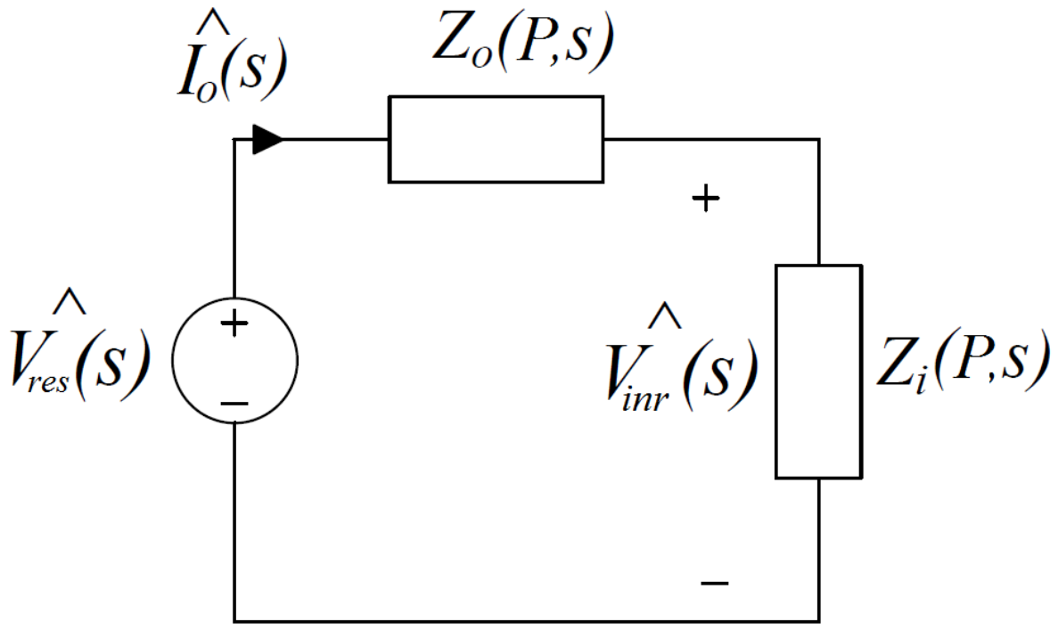
Figure 7 depicts the Thévenin’s model of the cascade connection of the LFR stage and the resonant inverter. Z o ( P , s ) is the output impedance of the LFR and Z i ( P , s ) is the input impedance of the inverter. From Figure 7, the following expression holds
v ^ i n r ( s ) v ^ r e s ( s ) = Z i ( P , s ) Z i ( P , s ) + Z o ( P , s ) = 1 1 + Z o ( P , s ) Z i ( P , s )
Therefore, the stability condition can be expressed as follows
ω , Z o ( P , j ω ) Z i ( P , j ω ) < 1 if ω p where Z o ( P , j ω ) Z i ( P , j ω ) = 1 arg Z o ( P , j ω ) Z i ( P , j ω ) 180 deg .
Moreover, from (27) and (28) it is derived
v ^ r e s ( s ) = A ( s ) v ^ g ( s ) + B ( s ) g ^ ( s )
Z o ( P , s ) = v ^ C ( s ) i ^ o ( s ) = v ^ r e s ( s ) i ^ r e s ( s ) = 1 C s + I r e s 2 C V g 2 G = 1 C s + 1 Z D C ( P ) C
Besides, the resonant inverter input impedance Z i ( P , s ) is given by
Z i ( P , s ) = Z l a m p ( P , s ) L s C s s 2 + ( C p + C s ) s + L s C s s 2 + 1 C s s Z l a m p ( P , s ) C p s + 1
where Z l a m p ( P , s ) must be replaced by expression (24) in case of using a HPS or MH lamp, or by (25) in case of an IEFL lamp.
It is worth remarking that the validity of the small-signal analysis depends on the linearity of the dynamics of the system. In this sense, when a lamp is operated at high frequency its dynamic behavior is much more linear than when operated at small frequency, thus extending the validity of the small-signal models. As an example, the voltage and current waveforms in a discharge lamp are much less distorted, and more sinusoidal, when they are supplied at 50 kHz than when are driven at 50 Hz [15].
Also, it is worth mentioning that the boost output impedance has low-pass filter characteristics, which ensures the system rejection to high-frequency perturbations, i.e., the higher is the frequency of a possible perturbation, less is the boost converter affected. Moreover, the resonant tank is used to transfer the power to the lamp at high frequency, between ω s and ω o , just within that frequency band where the boost output impedance is much lower than at zero frequency.
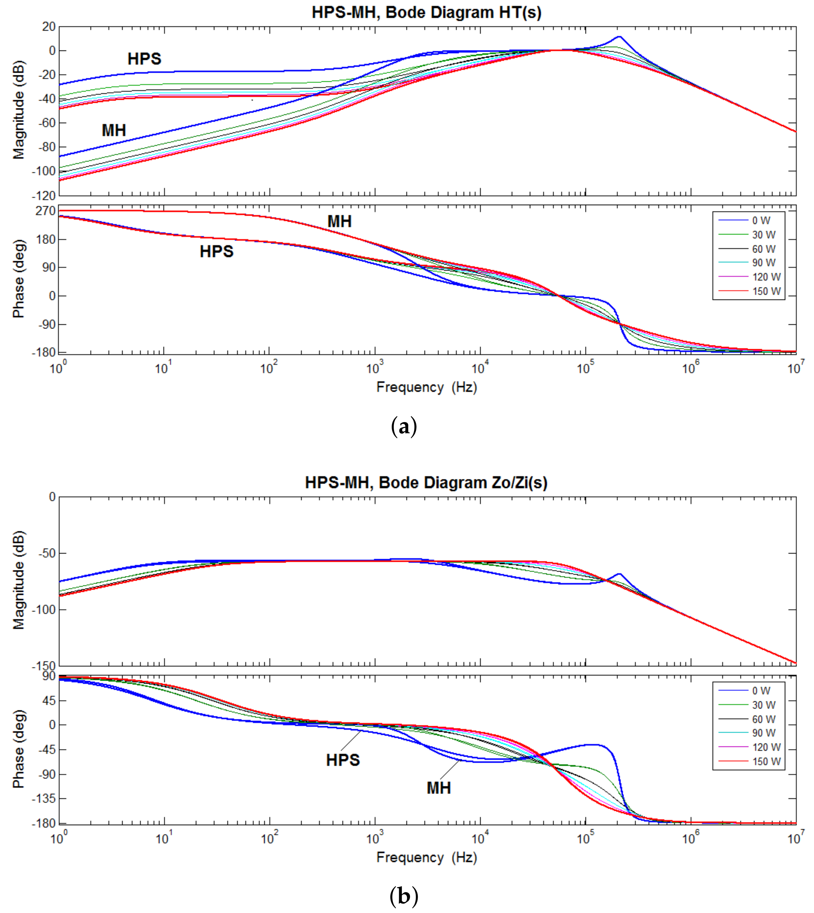
The Bode diagrams depicted in Figure 8a and Figure 9a have been plotted using the data of Table 1 and Table 2 respectively. Two cases can be distinguished in Figure 8a depending on the position of the pole p L and zero z L of the lamp. As it can be seen in the Bode diagram of Figure 8b, and according to (35), the stability of the ballast is not affected by changes in z L and p L over a wide range. As an example, according to Table 1, the ratio between the pole positions of the MH and HPS cases is p L ( M H ) / p L ( H P S ) 570 and the ratio between zeros is z L ( M H ) / z L ( H P S ) 0.588 . The values of Table 2 and Figure 9b correspond to an ENDURA IEFL lamp used in the experiments. The overall result, shown in Figure 8b and Figure 9b proves that | Z o ( ω ) / Z i ( ω ) | is well below 0 dB, which ensures the stability of the cascade connection.

5. Ballast Realization and Experimental Results

This section shows the experimental realization of the proposed universal ballast and demonstrates its performance for a set of representative lamps. The details of the different parts of the ballast are described first. Then, the steady-state and transient waveforms of the ballast in different operating conditions, including dimming, are shown.

5.1. Realization of the First Stage

As shown in Figure 2, the ballast consists of two power stages. The first stage includes two parts: the boost converter and its controller. The boost converter, which is shown in Figure 10, behaves like an LFR thanks to the controller depicted in Figure 11. The converter main switch is based on the complementary action of two silicon carbide devices, the MOSFET Q1 (IRFP4768), and the diode D1 (SDP20S120D). The driver is implemented with two bipolar transistors, a npn transistor (ZTX 653) with a Vce of 100 V and a collector current of 2 A, and its complementary pair, the pnp transistor (ZTX 753). The MOSFET gate resistance is an E24 resistor of 2.2 Ω, and the parallel protection network consists of an E24 10 kΩ resistor and a 16 V 500 mW zener diode, model C16PH. The input series inductor of 20 μH has been made with 50 parallel strands of 0.07 mm2 to reduce the skin-effect and 17 turns around the Kool μ 77109-A7 core. The output capacitor involves two polypropylene capacitors of 20 μF each one (EPCOS B32926E3206M) with a breakdown voltage of 500 V connected in parallel with four ceramic capacitors of 1 μF and the same breakdown voltage.
The switch-driver input signal Q is activated by the hysteretic comparator as illustrated in Figure 11. In the control circuit, the input and output voltages are sensed by two voltage dividers, and the input current sensor is a Hall effect transductor model (LEM LA 55-P) with a bandwidth of 200 kHz. Signals Vin/10, Vboost/100, and IL/10 are proportional to the input voltage V g , the output voltage V r e s , and the inductor current i L respectively.
The controller, which can be seen in Figure 11, includes a maximum voltage reference block with overvoltage protection that sets the maximum boost voltage to V r e s = 230 V. This reference has been included to preclude the voltage increase in case of failure in the lamp strike, because in this case, the boost converter would remain unloaded. If the lamp start-up is successful, the boost voltage will never reach 230 V, and the integrator of the protection block will be saturated at 15 V supplying energy to the conductance block. On the contrary, if the lamp start-up fails when the boost voltage reaches 230 V, the input voltage of the conductance reference block will be set to zero, and the converter input current will become zero, avoiding output voltage overvoltage.
The controller also includes a potentiometer to adjust G, that is, the power delivered to the lamp. The remaining blocks of the controller include, an AD633 multiplier, a subtraction circuit to implement the sliding surface and the hysteretic comparator. This last part employs two LM319 comparators with a response time of 80 ns, and a JKMC14027 flip flop with a bandwidth of 13 MHz.

5.2. Realization of the Second Stage

The second stage, which is shown in Figure 12, consists of a full bridge and a L s C s C p resonant tank. The full bridge employs four MOSFETs (IRFP4768), featuring E24 gate resistances of 5 Ω, and a parallel protection network with a 1 kΩ resistance and the 16 V zener diode. Regarding the resonant tank, the L s series inductor has been built in-house, using a 14-strands 0.07 mm2 litz wire. The winding has 18 turns around a Molypermalloy 55868-A2 core. The series capacitor C s comprises two polypropylene capacitors of 12 nF and 10 nF (Vyshay) in parallel and with a breakdown voltage of 2 kV. Finally, the parallel capacitor C p consists of two 4 kV 6.8 nF polypropylene capacitors connected in series.
The switches are activated by two IR2110 drivers, whose inputs are given by a logic network, shown in Figure 13, which assures a minimum blanking-time between the high-side and low-side MOSFETs. Depending on the lamp and the mode of operation, the blanking delay network is activated at a given constant frequency by a voltage-controlled oscillator. As an example, conventional lamps (HPS or MH) can be started at the main resonant frequency ω o = 245 kHz, but are operated in steady-state at the series resonant frequency ω s = 90 kHz. The proposed oscillator is based on the ICL8038 analog function generator integrated circuit. By adding the npn transistor BC547, the 1N4148 diode, three resistors, and an LDR (light dependent resistance) the frequency of the oscillator is reduced automatically to 90 kHz during the first seconds of the lamp warm-up, before the lamp begins to change the color. Since the transformer coil of the IEFL lamp is designed to operate around 240 kHz, the LDR used to reduce the inverter switching frequency is not used in this case.

5.3. Experimental Results

Figure 14a shows the power stage of the ballast, whereas the four different discharge lamps used to test the ballast can be seen in Figure 14b. These lamps are: two 250 W metal-halide lamps (the HQI-T PRO with greenish light, and the I-Quarium DE-MH with bluish light), the 150 W HPS-T sodium vapor lamp with orange light, and the 150 W Endura IEFL lamp.
Figure 15 depicts the waveforms of voltages and currents at the input of the resonant converter and at the lamp, for four different lamp types. Three of the operational modes of the lamps are shown: strike, warm-up, and steady-state operation. The LFR controller ensures that the power delivered is 150 W for all lamps. This means that the IEFL and HPS lamps are tested at full power, whereas both 250 W MH lamps are tested at 60% of their rated power. As expected, the steady-state voltage of the IEFL lamp is higher than the voltages of other non-coil driven lamps. Also, it can be seen that HPS, HQI-T and DE-MH lamps suffer a sudden voltage and current transient when the inverter switching frequency changes from 220 kHz to 90 kHz.
To analyze the performance of the proposed ballast with different lamps, the ballast has been tested in steady-state at different power levels, which correspond to dimming operation: 50 W, 70 W, 100 W and 150 W of input power. To simplify the analysis, the input voltage is constant and equal to 12 V, and input power is adjusted by means of the LFR controller. Figure 16 shows: (a) the efficiency of the first boost-LFR stage, (b) the efficiency of the LCC inverter, (c) the overall ballast efficiency, (d) the boost-LFR switching frequency, (e) the boost-LFR output voltage, and (f) the voltage of the lamp. The overall efficiency of the lamp is well above 90% for most of the cases and power outputs, except for the IEFL case at full power. One of the reasons behind this is the voltage variation range of the IEFL lamp that under dimming operation is wider than in other lamps. The power efficiency of the proposed approach at similar power levels can be compared with single-stage ballasts ranging from 83% [12] to 93% [13] and conventional two-stage ballasts whose efficiencies are typically around 85% to 90% [14].
Details of the waveforms of the ballast under dimming operation are shown in Figure 17. Figure 17a,b show the IEFL and the HPS lamp operating at 75 W and 150 W (50% and 100% of their rated power). As expected, the resonant inverter works at 220 kHz with the IEFL lamp, whereas the switching frequency is 90 kHz when testing the HPS lamp. The figure also includes: (c) the 250 W HQI-T lamp shortly after the strike, at the warm-up beginning, (d) the same lamp operating at 150 W (60% of rated power), and (e) the aquarium 250 W DE-MH lamp operating at 150 W.

6. Conclusions

A two-stage electronic ballast to drive discharge lamps based on the LFR concept has been presented in this paper. The ballast behaves like an LFR, so it delivers the desired power to the lamp irrespective of the lamp impedance. This feature ensures the lamp operation at nominal power during all the lamp lifetime and allows an easy light-dimming. Design key issues have been discussed, and an experimental prototype has been realized. The tests with diverse HID lamps have proven the feasibility and versatility of the proposed approach, showing the design robustness, and a good agreement with the theoretical predictions. The ballast has been tested with IEFL, HPS and MH lamps. These experiments include start-up, warm-up transients, and steady-state operation. The ballast versatility has been shown also at full power and under dimming operation. The ballast global efficiency is in the range of 86–96%, and can be improved by means of using silicon carbide (SiC) or Gallium Nitride (GaN) devices.

Author Contributions

Conceptualization, H.V.-B.; Investigation, H.V.-B. and A.L.-M.; Validation, A.L.-M.; Visualization, C.O. and À.C.-P.; Writing—original draft, H.V.-B. and A.L.-M.; Writing—review & editing, C.O. and À.C.-P.

Funding

The research leading to these results has received funding from the Spanish AEI agency under grants DPI2015-67292-R and DPI2017-84572-C2-1-R.

Acknowledgments

The authors would like to acknowledge the contribution of Xavier Genaro-Muñoz for his support in the experimental validation of the ballast.

Conflicts of Interest

The authors declare no conflict of interest. The founding sponsors had no role in the design of the study; in the collection, analyses, or interpretation of data; in the writing of the manuscript, and in the decision to publish the results.

References

  1. UN Environment—Global Environmental Facility. Accelerating the Global Adoption of Energy-Efficient Lighting. Available online: http://wedocs.unep.org/bitstream/handle/20.500.11822/20406/Energy_efficient_lighting.pdf (accessed on 27 March 2019).
  2. Steiner, A. The Transition to Energy Efficient Lighting is One of the Most Straightforward and Cost-Effective Approaches to Significantly Reduce the Threat of Global Climate Change. Available online: https://www.unenvironment.org/news-and-stories/story/brighten-making-switch-efficient-lighting (accessed on 27 March 2019).
  3. Philips QL Induction Lighting Systems: Information for Original Equipment Manufacturers. Available online: https://www.stefanslichtparade.de/files/ql_oem_guide.pdf (accessed on 20 January 2019).
  4. Piper, J.E. Operations and Maintenance Manual for Energy Management; Sharpe Professional; Routledge: New York, NY, USA, 2009. [Google Scholar]
  5. Osram Endura Datasheet. The High Performance Electrodelesss Fluorescent Lamp. Available online: https://www.osram.com/media/resource/HIRES/333886/554635/ENDURA-QUICKTRONIC-System-QT-ENDURA.pdf (accessed on 21 January 2019).
  6. Godyak, V.A. Bright idea, radio-frequency light sources. IEEE Ind. Appl. Mag. 2002, 8, 42–49. [Google Scholar] [CrossRef]
  7. Rubinstein, F.; Siminovitch, M.; Verderber, R. Fifty percent energy savings with automatic lighting controls. IEEE Trans. Ind. Appl. 1993, 29, 768–773. [Google Scholar] [CrossRef]
  8. Waymouth, J.F. Electric Discharge Lamps; MIT Press: Cambridge, MA, USA, 1971. [Google Scholar]
  9. Stevenson, R. The LED’s Dark Secret: Solid-state lighting won’t supplant the lightbulb until it can overcome the mysterious malady known as droop. IEEE Spectrum. 2009. Available online: https://spectrum.ieee.org/semiconductors/optoelectronics/the-leds-dark-secret (accessed on 9 April 2019).
  10. Alonso, J.M.; Rico, M.; Blanco, C.; Lopez, E. A novel low-loss clamped-mode LCC resonant inverter for HID lamp supply. In Proceedings of the PESC’95-Power Electronics Specialist Conference, Atlanta, GA, USA, 18–22 June 1995; Volume 2, pp. 736–742. [Google Scholar]
  11. Cardesin, J.; Alonso, J.M.; Lopez-Corominas, E.; Calleja, A.J.; Ribas, J.; Rico-Secades, M.; Garcia, J. Small-signal analysis of a low-cost power control for LCC series-parallel inverters with resonant current mode control for HID lamps. IEEE Trans. Power Electron. 2005, 20, 1205–1212. [Google Scholar] [CrossRef]
  12. Marchesan, T.B.; Dalla-Costa, M.A.; Alonso, J.M.; Prado, R.N.D. Integrated Zeta-Flyback Electronic Ballast to Supply High-Intensity Discharge Lamps. IEEE Trans. Ind. Electron. 2007, 54, 2918–2921. [Google Scholar] [CrossRef]
  13. Giezendanner, F.; Biela, J.; Kolar, J.W. Optimization and Performance Evaluation of an AC-Chopper Ballast for HPS Lamps. IEEE Trans. Ind. Electron. 2014, 61, 2236–2243. [Google Scholar] [CrossRef]
  14. Azcondo, F.J.; Diaz, F.J.; Brañas, C.; Casanueva, R. Microcontroller Power Mode Stabilized Power Factor Correction Stage for High Intensity Discharge Lamp Electronic Ballast. IEEE Trans. Power Electron. 2007, 22, 845–853. [Google Scholar] [CrossRef]
  15. Brañas, C.; Azcondo, F.J.; Bracho, S. Electronic ballast for HPS lamps with dimming control by variation of the switching frequency. Soft start-up method for HPS and fluorescent lamps. In Proceedings of the 24th Annual Conference of the IEEE Industrial Electronics Society (IECON), Aachen, Germany, 31 August–4 September 1998; pp. 953–958. [Google Scholar]
  16. Jang, T.; Kim, H.; Kim, H. Dimming Control Characteristics of Electrodeless Fluorescent Lamps. IEEE Trans. Ind. Electron. 2009, 56, 93–100. [Google Scholar] [CrossRef]
  17. Fraytag, J.; Schlittler, M.E.; Costa, M.A.D.; Seidel, A.R.; Alonso, J.M.; Prado, R.N.D.; Silva, M.F.D. A Comparative Performance Investigation of Single-Stage Dimmable Electronic Ballasts for Electrodeless Fluorescent Lamp Applications. IEEE Trans. Power Electron. 2015, 30, 2239–2252. [Google Scholar] [CrossRef]
  18. Silva, M.F.D.; Fraytag, J.; Marchesan, R.; Rosa, V.L.; Costa, M.A.D.; Alonso, J.M.; Prado, R.N.D. A dimmable Cuk half-bridge single-stage converter applied to electrodeless fluorescent lamps. In Proceedings of the 2012 15th International Power Electronics and Motion Control Conference (EPE/PEMC), Novi Sad, Serbia, 4–6 September 2012; pp. DS1b.6-1–DS1b.6-5. [Google Scholar]
  19. Silva, M.F.D.; Fraytag, J.; Schlittler, M.E.; Marchesan, T.B.; Costa, M.A.D.; Alonso, J.M.; Prado, R.N.D. Analysis and Design of a Single-Stage High-Power-Factor Dimmable Electronic Ballast for Electrodeless Fluorescent Lamp. IEEE Trans. Ind. Electron. 2013, 60, 3081–3091. [Google Scholar] [CrossRef]
  20. Schlittler, M.E.; Fraytag, J.; Seidel, A.R.; Alonso, J.M.; Prado, R.N.D.; Chagas, N.B.; Silva, M.F.D. Comparison between integrated and non-integrated SEPIC half-bridge electronic ballasts for electrodeless fluorescent lamp applications. In Proceedings of the 2013 Brazilian Power Electronics Conference, Gramado, Brazil, 27–31 October 2013; pp. 1201–1206. [Google Scholar]
  21. Silva, M.F.D.; Chagas, N.B.; Schlittler, M.E.; Fraytag, J.; Marchesan, T.B.; Bisogno, F.E.; Alonso, J.M.; Prado, R.N.D. Electric Equivalent Model for Induction Electrodeless Fluorescent Lamps. IEEE Trans. Power Electron. 2013, 28, 3603–3613. [Google Scholar] [CrossRef]
  22. Singer, S. Realization of loss-free resistive elements. IEEE Trans. Circuits Syst. 1990, 37, 54–60. [Google Scholar] [CrossRef]
  23. Singer, S.; Erickson, R.W. Canonical modeling of power processing circuits based on the POPI concept. IEEE Trans. Power Electron. 1992, 7, 37–43. [Google Scholar] [CrossRef]
  24. Haroun, R.; Cid-Pastor, A.; Aroudi, A.E.; Martinez-Salamero, L. Synthesis of Canonical Elements for Power Processing in DC Distribution Systems Using Cascaded Converters and Sliding-Mode Control. IEEE Trans. Power Electron. 2014, 29, 1366–1381. [Google Scholar] [CrossRef]
  25. Kirsten, A.L.; Hansen, J.; Luz, P.C.V.D.; Rech, C.; Prado, R.N.D.; Costa, M.A.D. Modeling and control strategy of HPS electronic ballast considering the dynamic model of the lamp. In Proceedings of the XI Brazilian Power Electronics Conference, Praiamar, Brazil, 11–15 September 2011; pp. 1–6. [Google Scholar]
  26. Costa, M.A.D.; Kirsten, A.L.; Alonso, J.M.; Garcia, J.; Gacio, D. Analysis, Design, and Experimentation of a Closed-Loop Metal Halide Lamp Electronic Ballast. IEEE Trans. Ind. Appl. 2006, 48, 28–36. [Google Scholar] [CrossRef]
  27. Leon-Masich, A.; Valderrama-Blavi, H.; Bosque-Moncusi, J.M.; Maixe-Altes, J.; Martinez-Salamero, L. Sliding-Mode-Control-Based Boost Converter for High-Voltage Low-Power Applications. IEEE Trans. Ind. Electron. 2014, 62, 229–237. [Google Scholar] [CrossRef]
Figure 1. Block diagram of the LFR-based electronic ballast.
Energies 12 01403 g001
Figure 2. Two-stage ballast block diagram. Sliding-mode controlled boost converter in cascade with LsCsCp full bridge resonant inverter.
Energies 12 01403 g002
Figure 3. Boost converter states. (a) ON-state; and (b) OFF-state.
Energies 12 01403 g003
Figure 4. Boost converter, LFR-based small-signal model.
Energies 12 01403 g004
Figure 5. IEFL: (a) lamp construction, (b) electrical model (from [21]).
Energies 12 01403 g005
Figure 6. Resonant tank gain and design criteria.
Energies 12 01403 g006
Figure 7. Thévenin’s model of the cascade connection of both ballast stages, the boost-LFR, and the LCC resonant inverter.
Energies 12 01403 g007
Figure 8. Frequency response of H T ( P , s ) and Z o ( s ) / Z i ( s ) for the HPS and MH cases. (a) Bode Diagram of H T ( P , s ) = v ^ l a m p ( s ) / V ^ A B ( s ) ; (b) Bode Diagram of Z o ( s ) / Z i ( s ) .
Energies 12 01403 g008
Figure 9. Frequency response of H T ( P , s ) and Z o ( s ) / Z i ( s ) for the IEFL case. (a) Bode Diagram of H T ( P , s ) = v ^ l a m p ( s ) / V ^ A B ( s ) ; (b) Bode Diagram of Z o ( s ) / Z i ( s ) .
Energies 12 01403 g009
Figure 10. Detail of the circuit realization of the first stage (boost converter) of the ballast.
Energies 12 01403 g010
Figure 11. Schematic of the controller of the first stage.
Energies 12 01403 g011
Figure 12. Detail of the circuit realization of the second stage (inverter) of the ballast.
Energies 12 01403 g012
Figure 13. Schematic of the controller of the second stage.
Energies 12 01403 g013
Figure 14. Pictures of the experimental setup. (a) Converters of the ballast; (b) Lamp test-bed.
Energies 12 01403 g014
Figure 15. Waveforms of V C , V l a m p and I r e s showing strike, warm-up, and steady operation at 150 W with the four different lamps: (a) 250 W HQI-T PRO (greenish light MH); (b) 250 W I-Quarium DE-MH (bluish light MH); (c) 150 W HPS-T Basic Plus (orange light); and (d) 150 W IEFL Endura Luminarc (white light).
Energies 12 01403 g015
Figure 16. Figures of merit of the proposed universal ballast. (a) First Stage (Boost-LFR) Efficiency; (b) Second Stage (Inverter) Efficiency; (c) Overall Efficiency; (d) Switching Frequency of the First Stage; (e) Output Voltage of the First Stage; (f) Output Voltage of the Second Stage.
Energies 12 01403 g016
Figure 17. Detail of dimming operation of the ballast with different lamps. (a) 150 W IEFL under dimming operation: 75 W (half) and 150 W (full power); (b) 150 W HPS under dimming operation: 75 W (half) and 150 W (full power); (c) 250 W HQI-T after strike; (d) 250 W HQI-T at 60% of the rated power; (e) 250 W DE-MH at 60% of the rated power.
Energies 12 01403 g017
Table 1. Simulated ballast behavior with a given HPS and MH lamp.
P30 W60 W90 W120 W150 W
f s = 2 π ω s 90 kHz
HPS z L = −3141.5 rad/s and p L = 18.8 rad/s
MH z L = −1850 rad/s and p L = 10,690 rad/s
R L 225 Ω135 Ω100 Ω79.5 Ω65.4 Ω
V l a m p 82.2 V90.4 V95 V97.8 V99 V
| H T ( j ω s ) | 1.131.050.960.880.81
| V r e s | = V c 80.7 V95.5 V110 V123 V135 V
I r e s 0.37 A0.673 A0.82 A0.98 A1.11 A
Z D C ( P ) 218 Ω151 Ω134 Ω125 Ω121 Ω
Table 2. Simulated ballast behavior for the IEFL lamp used in the experiments.
P30 W60 W90 W120 W150 W
f s = 2 π ω s 220–230 kHz
R C 29 kΩ34 kΩ33 kΩ32 kΩ30 kΩ
R L 5 kΩ1.47 kΩ570 Ω410 Ω425 Ω
L C 66 μH59 μH56 μH48 μH40 μH
C L 380 pF340 pF240 pF100 pF110 pF
V l a m p 357 V291 V224 V221 V250 V
| H T ( j ω s ) | 8.596.452.872.082.12
V r e s 46.1 V50.1 V86.7 V118 V131 V
I r e s 0.65 A1.2 A1.03 A1.02 A1.14 A
Z D C ( P ) 71 Ω42 Ω84 Ω120 Ω115 Ω

