Article

Digital Control of a Buck Converter Based on Input-Output Linearization. An Interpretation Using Discrete-Time Sliding Control Theory

1
Departament d’Enginyeria Electrònica, Elèctrica i Automàtica, Escola Tècnica Superior d’Enginyeria, Universitat Rovira i Virgili, 43007 Tarragona, Spain
2
Department of Electromechanics and Energy Conversion, Universidad de Talca, Curicó 3340000, Chile
*
Author to whom correspondence should be addressed.
Energies 2019, 12(14), 2738; https://doi.org/10.3390/en12142738
Submission received: 14 June 2019 / Revised: 8 July 2019 / Accepted: 16 July 2019 / Published: 17 July 2019
(This article belongs to the Special Issue Sliding Mode Control of Power Converters in Renewable Energy Systems)

Abstract

:
This paper presents the analysis and design of a PWM nonlinear digital control of a buck converter based on input-output linearization. The control employs a discrete-time bilinear model of the power converter for continuous conduction mode operation (CCM) to create an internal current control loop wherein the inductor current error with respect to its reference decreases to zero in geometric progression. This internal loop is as a constant frequency discrete-time sliding mode control loop with a parameter that allows adjusting how fast the error is driven to zero. Subsequently, an outer voltage loop designed by linear techniques provides the reference of the inner current loop to regulate the converter output voltage. The two-loop control offers a fast transient response and a high regulation degree of the output voltage in front of reference changes and disturbances in the input voltage and output load. The experimental results are in good agreement with both theoretical predictions and PSIM simulations.

Graphical Abstract

1. Introduction

Since breaking into the regulation of dc-dc switching converters at the end of the 1990s, the digital control has undergone successive phases of expansion and stagnation. Destined to be a new standard for the switching converters at the moment of its appearance, the reality, however, has shown that its adoption by the industry has been so far practically inexistent. Despite the inherent advantages of the digital control such as insensitivity to noise, design reuse and reprogram capability, the user’s mistrust, on the one hand, and the difficulty of design, on the other hand, have contributed to this absence of industrial penetration [1].
From the user’s perspective, adopting a new technology more expensive than the present one and not working so well in terms of accuracy in steady-state and dynamic performance was a risk that the manufacturers did not want to take. Time-delay and numerical limit cycles are intrinsic drawbacks associated with the digital design that eventually degrade the controller’s response. The time-delay problem is introduced mainly by the analog-to-digital converter in the cycle by cycle realization of the sampling/conversion process [2,3], which provokes a controller’s delayed reaction of one switching cycle. To mitigate this problem, the sampling/conversion process is performed at large sampling rates up to 32 times the switching frequency [4,5] and small quantization steps are often employed, which results in an increasing of cost, hardware complexity and consumption of the controller. The limit cycle issue is caused by the digital pulse width modulator and the quantization error of the analog-to-digital converter, this yielding an oscillation in the converter output voltage [6].
From the designer’s point of view, the realization of the digital controller is less intuitive than the corresponding analog implementation. In addition to this fact, it has to be pointed out that the first designs required silicon areas considerably bigger than those needed presently and their power consumption was significantly larger than that of their corresponding analog counterparts. However, the exponential decrease of cost and size of digital circuits, which in the period elapsed since 1998 has dramatically incremented the capacity of integrating electronic functions, has revived the idea of digital control as the definitive substitute of the analog equivalent in dc-dc switching converters. This idea is being supported by the fact that recent digital research has been focused on non-realizable aspects in the analog domain such as integrating communications, controller’s self-tuning, converter’s efficiency monitoring and complex nonlinear control techniques implementation. An example of this are the works reported in [5,7], where the dynamic response to perturbations in the power converter is improved by a specific nonlinear control with self-tuning and the overall performance is ameliorated by the action of an active efficiency monitoring system. Other contributions have dealt with new modulation schemes [8] to optimize the converter’s efficiency and extend its input range. Some recent reports are also found when testing new complex control strategies either deterministic [9] or random modulation-based [10], and in introducing new on-line self-tuning protocols [11].
Most digital control realizations are of hybrid type, which means that they combine the action of a nonlinear controller to facilitate a fast transient response with the performance of a linear controller to obtain a precise regulation in steady-state. This is the case of [12], wherein a fuzzy logic-based controller implements a PI algorithm to eliminate the output voltage error in steady-state. However, when that error or its time derivative are relatively high, the duty cycle changes rapidly by means of a nonlinear action. A similar situation is described in [5], where a PID algorithm for steady-state regulation is combined with a sliding mode control for minimum time transient operation. A posterior attempt to solve the problem of minimum time transient recovery is reported in [13] together with a concise description of different strategies dealing with this problem. Nevertheless, the controller does not operate on-line because it only uses memory accesses and comparisons of previously stored data. Another approach on minimization concerns the output deviation as reported in [14], where a specific integrated circuit for a digital control of a single and a two-phase buck converters is introduced showing that the deviation of the output is four times smaller than that of a fast PID compensator. Other cases exhibiting this hybrid nature are found in the optimal-time control whose goal is to lead the converter’s dynamics to the steady-state in minimum time [15], in the near-optimal voltage deviation and recovery time [16,17], and finally in the use of a hysteretic analog modulator together with a digital linear control loop and a digital frequency regulation loop [18].
On the other hand, most linear digital controllers have been designed from linear analog controllers by mapping the s-plane into the z-plane and employing either frequency domain methods or pole-zero assignments in the z-plane. The first exception is the work reported in [19], where the controller design is based on a discrete-time linear model of the plant, which is obtained with the method presented in [20] for switching converters operating in continuous conduction mode with constant switching frequency. A second exception is found in [21], where a time-domain design method is used to fit a digital PID template to the desired response. In [22], after a review of previous contributions, a methodology to design non-linear digital controllers based on discrete-time sliding mode control is presented where a dead-beat response is achieved [23]. Also, in [24] this methodology is applied to regulate the output voltage of a boost converter with constant power load, providing a comparison with one of the most referenced works in digital control of power converters [25].
The aim of this work is to develop a digital control that combines a good transient response and a good steady-state regulation in only one algorithm. This has the advantage of simplifying the control implementation with respect to the hybrid control realizations found extensively in the literature. The starting point of the controller proposed in this article is the bilinear recurrence developed in [26] for PWM converters in CCM, which is reviewed in Section 2. The proposed nonlinear controller is obtained by input-output linearization and presented in Section 3, in which a discrete-time sliding mode interpretation is also provided. Output voltage regulation and experimental results are reported in Section 4 and Section 5 respectively. Conclusions are presented in Section 6.

2. Nonlinear Recurrence

The dynamic behaviour of a dc-to-dc switching converter operating in CCM with constant switching frequency can be described by the following pair of state equations
X ˙ = A 1 X + b 1 V g n T t < ( n + d n ) T
X ˙ = A 2 X + b 2 V g ( n + d n ) T t < ( n + 1 ) T
where X is the converter state vector, A 1 , A 2 , b 1 , and b 2 are constant-coefficient matrices, T is the switching period, n T is the instant at the beginning of the conduction state (“ON” state) in n t h cycle, and d n T is the duration of “ON” state. Let d n the duty cycle during the switching cycle ( n T , ( n + 1 ) T ) and d ¯ n = 1 d n .
The solution of the first equation with initial condition X ( n T ) is given by
X ( ( n + d n ) T ) = e A 1 d n T X ( n T ) + n T ( n + d n ) T e A 1 ( ( n + d n ) T ζ ) b 1 V g d ζ .
Taking into account that the pair [ A i , e A i t ] commutes, i.e., A i 1 e A i t = e A i t A i 1 , Equation (3) becomes as follows
X ( ( n + d n ) T ) = e A 1 d n T X ( n T ) + e A 1 d n T I A 1 1 b 1 V g
where I is a unitary matrix with appropriate dimensions. Similarly, the solution of Equation (2) with initial condition X ( ( n + d n ) T ) will be given by Equation (5),
X ( ( n + 1 ) T ) = e A 2 d ¯ n T X ( ( n + d n ) T ) + ( n + d n ) T ( n + 1 ) T e A 2 ( ( n + 1 ) T ζ ) b 2 V g d ζ .
By inserting Equation (4) in (5) we obtain
X ( ( n + 1 ) T ) = e A 2 d ¯ n T [ e A 1 d n T X ( n T ) + ( e A 1 d n T I ) A 1 1 b 1 V g ] + ( e A 2 d ¯ n T I ) A 2 1 b 2 V g .
Please note that terms in the form ( e A T I ) A 1 have a matrix series expansion even if A is singular
( e A T I ) A 1 = T n = 0 ( A T ) n ( n + 1 ) ! .
In practice, the switching frequency is much larger than the natural frequencies of the power converters and therefore the exponential matrices containing T can be approximated by their respective first terms of a Taylor’s series at T = 0 , so that Equation (6) can be written as follows in (8),
X ( ( n + 1 ) T ) [ I + ( A 1 d n + A 2 d ¯ n ) T ] X ( n T ) + ( b 1 V g d n + b 2 V g d ¯ n ) T ] .
The recurrence equation defined in Equation (8) can be expressed as
X ( ( n + 1 ) T ) = H X ( n T ) + F X ( n T ) d n T + E d n T + G
where
E = b 1 b 2 V g , F = A 1 A 2 , G = b 2 V g T , H = I + A 2 T .
The nonlinear nature of recurrence Equation (9) is observed in the second and forth terms by showing the respective multiplication of the duty cycle (control) by the state vector and by an additive term depending on the input voltage (energy). In the particular case of the buck converter A 1 = A 2 , which implies F = 0 and reveals that the nonlinear behaviour is an afine characteristic. In the case of a boost converter b 1 = b 2 , which results in E = 0 and shows that the nonlinear characteristic is produced by the product of the control and state vector.
Although a constant value has been considered for V g , the analysis developed could be applied also to slowly varying input voltages. In this case there will be also a nonlinearity produced by the product of the control and the input voltage.

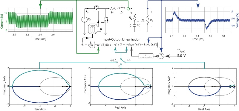
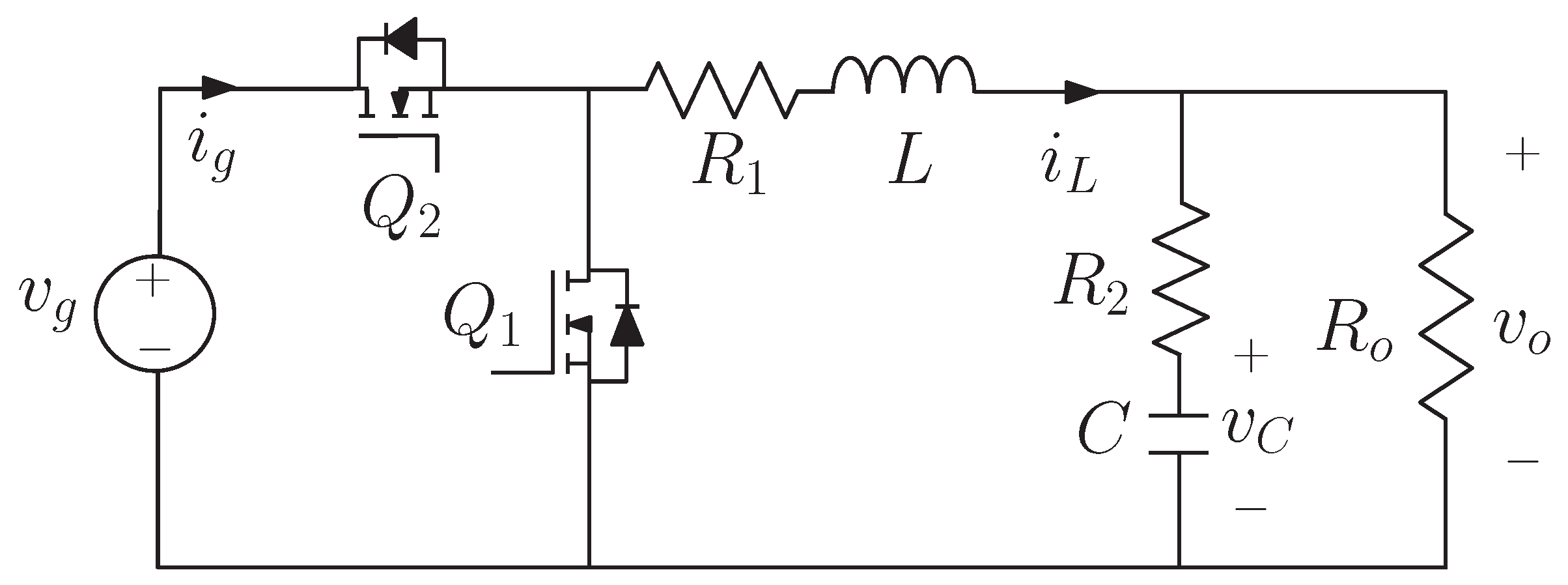
3. Current Control Loop Based on Input-Output Linearization

In the particular case of a buck converter (Figure 1), the state vector is X = [ v C i L ] T and therefore the nonlinear recurrence can be simplified as follows
X ( ( n + 1 ) T ) = H X ( n T ) + E d n T
since F and G are zero because A 1 = A 2 and b 2 = 0 in such converter.
Matrix H can be expressed as
H = h i j 2 × 2
where
h 11 = 1 R a T L , h 12 = ( 1 ε ) T L , h 21 = ( 1 ε ) T C , h 22 = 1 T C R b
and
R a = R 1 + R o R 2 R o + R 2 , ε = R 2 R o + R 2 , and R b = R o + R 2 .
Hence, recurrence Equation (11) can be expressed as
i L ( ( n + 1 ) T ) = h 11 i L ( n T ) + h 12 v C ( n T ) + V g L d n T
v C ( ( n + 1 ) T ) = h 21 i L ( n T ) + h 22 v C ( n T ) .
Now, let’s impose that the current sample at instant ( n + 1 ) T reaches a reference i R E F ( n T ) with an approximation error dynamics that decreases in geometric progression. The error dynamics can be expressed as follows
i L ( n + 1 ) T i R E F ( n T ) = w i L n T i R E F ( n T )
where
1 < w < 1
and w is the ratio of the decreasing geometric progression. Taking into account Equation (15), imposing the current error dynamics given by Equation (17) requires a control law given by
d n = L V g T ( ( 1 w ) i R E F ( n T ) h 12 v C ( n T ) ( h 11 w ) i L ( n T ) ) .
Assuming that the current has tracked its digitally generated reference of constant value i R E F ( n T ) = I R E F u ( n T ) = i R E F [ n ] for the sake of simplicity, the remaining dynamics corresponding to the capacitor voltage will be described by
v C ( ( n + 1 ) T ) = h 21 i R E F [ n ] + h 22 v C ( n T ) .
Besides, the converter parameters have the following bounds
0 < h 11 < 1 , 0 < h 22 < 1 , h 12 < 0 , and h 21 > 0 .
Therefore the coefficient of v C ( n T ) in recurrence Equation (20) is positive and smaller than one. Hence, the recurrence will always exhibit a stable behaviour around the converter steady-state operating point given by
I L = I R E F
V C = I R E F h 21 1 h 22
D = I R E F L V g T ( 1 h 22 ) ( 1 h 11 ) h 12 h 21 ( 1 h 22 ) .
It has to be pointed out that the recurrence based on the current valley is accurate to describe the inductor current dynamics but it is less exact to explain the capacitor voltage behaviour. This discrepancy is due to the ripple existence in both inductor current and capacitor voltage. Thus, if no losses are assumed, the steady-state mean value of the capacitor voltage will be given by the product of the corresponding mean value of the inductor current and the load resistance. This is not the case in Equation (23), which predicts a capacitor voltage given by the product of the current valley and the load resistance V C = R o I R E F . Hence, there is a prediction error in each recurrence period given by
V C V C = I M A X I R E F 2 R o
where V C and I M A X are the mean and maximum values of capacitor voltage and inductor current in steady-state respectively.
For this reason, the recurrence expressing the voltage behaviour is now modified with the introduction of some additional terms corresponding to a trapezoidal approximation in the calculation of the inductor current mean value. For the sake of simplicity, no losses are considered ( R 1 = 0 , R 2 = 0 ) so that the new recurrence for the capacitor voltage can be expressed as follows:
v C ( ( n + 1 ) T ) = h 21 i R E F [ n ] + h 22 v C ( n T ) + ( d n 2 + 2 d n ) T 2 2 L C V g
where d n was given in Equation (19), h 21 = T C , and h 22 = 1 T R o C T 2 2 L C .
The new equilibrium point is
I L = I R E F
V C = V g 2 ( 1 2 L R o T ) + 1 2 L R o T 2 + 8 L I R E F T V g
D = V C V g ,
which is coincident with the reported in [22] using an equivalent discrete-time sliding approach to obtain the recurrence for the output capacitor voltage. In fact, both approaches are completely equivalent if w = 0 . It is possible to provide a sliding mode interpretation of our approach Equation (17) considering that it proposes a more general switching surface s e than the one in [22], which was the current error with negative sign. The new surface Equation (31) includes a dynamical term of the current error with the same decreasing geometric progression of the input-output linearization and becomes Equation (30) for w = 0 .
s ( n T ) = i L ( n T ) I R E F ( n T )
s e ( n T ) = s ( n T ) w s ( ( n 1 ) T )
s e ( ( n + 1 ) T ) = 0 .
Adding a dynamical term in the discrete recurrence increases the order of the closed loop reference-to-current transfer function in the z domain Equation (34) that, since it exhibits the order reduction associated with sliding mode ideal dynamics, is of first order and can be directly determined from the recurrence equation of the current.
i L ( ( n + 1 ) T ) = w i L ( n T ) + ( 1 w ) I R E F ( n T )
G I ( z ) = I L ( z ) I R E F ( z ) = 1 w z w .
Please note that with w = 0 the pole of the I R E F -to- I L current loop transfer function is located at the origin like in a dead-beat control of a first order discrete-time system [23].

4. Voltage Regulation

An outer loop establishing the reference of the inner current loop is added now in order to regulate the output voltage to a desired level V R E F , the reference being the sum of two terms which are respectively proportional to the output voltage error and to the integral of the error.
In the descriptive equations of the system, Equations (17), (19), and (26), the discrete current reference, and proportional and integral errors can be expressed as follows
i R E F [ n ] = k 1 e [ n ] + k 2 i n t e [ n ] e [ n ] = V R E F u ( n T ) v C ( n T ) i n t e [ n ] = i n t e [ n 1 ] + e [ n ]
where V R E F is the desired output voltage and k 1 , k 2 are respectively the proportional and integral coefficients of the voltage regulation loop. Equivalently, Equation (35) can be written in compact form as
i R E F [ n ] = i R E F [ n 1 ] + k n k V I ( e [ n ] β z P e [ n 1 ] )
where the control parameters have been normalized with respect to Equation (13) as k n = ( k 1 + k 2 ) k V I and β = k 1 ( k 1 + k 2 ) z P .
It can be observed that, although the equation corresponding with the voltage regulator is linear, Equations (17), (19), (26) should be linearized around the equilibrium point so that the choice of coefficients k 1 , k 2 or k n , β can be carried out by means of linear control techniques. The analysis of the linearized equations together with Equation (35) in the z domain results in the following transfer equations
G P ( z ) = V C ( z ) I R E F ( z ) = k V I ( 1 w ) ( z z D ) ( z w ) ( z z P ) = G I ( z ) k V I ( z z D ) ( z z P )
G C ( z ) = I R E F ( z ) E ( z ) = k n h V I ( z β z P ) ( z 1 )
where coefficients k V I , z N and z P are
k V I = T ( V g V C ) C V g 0 z D = V C V g V C < 0 z P = 1 2 L T + R o T 2 ( 2 V C / V g 1 ) 2 L R o C .
It should be noted that the transfer function in Equation (37) presents a zero depending on the operating point associated with the delay inherent to the digitally PWM controlled converter [22].
The closed loop gain will be
T ( z ) = k n ( 1 w ) ( z z D ) ( z β z P ) ( z w ) ( z z P ) ( z 1 )
where β = 1 will fix a closed loop pole in its open loop position. A sensible design of the control parameters will usually consider the ranges 0 < β < 1 and 0 < k n .
Let us consider the converter coefficients and operation point described in [22]. It can be shown that z D = 1 for D = 0.5 ( V C = V g / 2 ) and the pole z P in the plant Equation (37) corresponds to the converter coefficient h 22 . For the given voltage operation point, while the previous zero and pole of the plant are already determined from the point of view of the controller design, the pole at w corresponding to the input-output linearization in the current loop can be adjusted to improve the performance of the voltage controller. Applying the Jury criterion to the characteristic equation 1 + T ( z ) = 0 the following expression can be obtained.
1 + w ( 1 w ) h 22 < k n β < 1 h 22 .
In the most restrictive case ( w 1 ) Equation (41) becomes
0 < k n < 1 β h 22 .
Other necessary conditions provided by the Jury criterion have been omitted because they are more complex and not so useful for the control design.

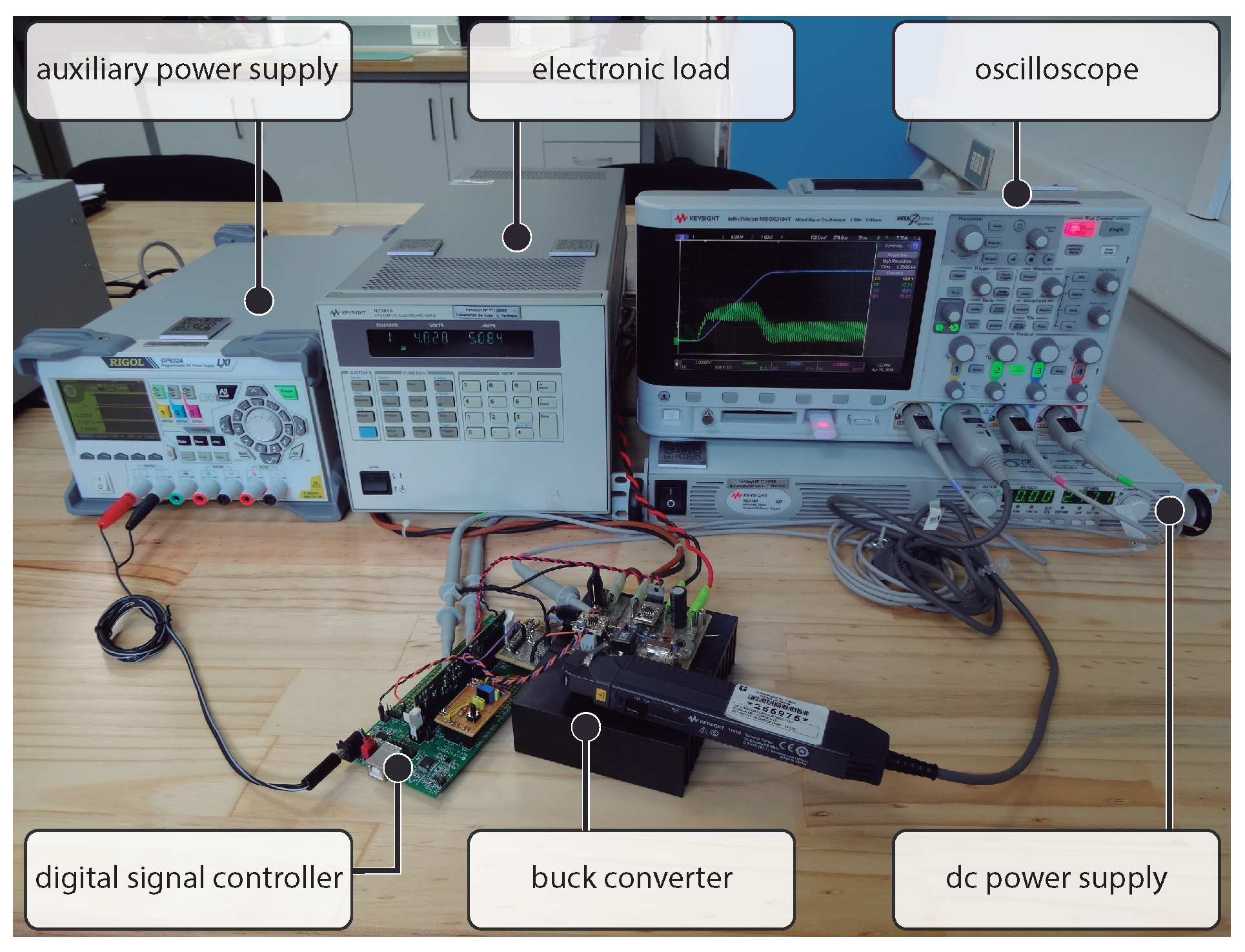
5. Experimental Results and Numerical Simulations

To verify the performance of the proposed digital control and, in particular, the effects of the inner current loop parameter w, a buck converter power stage with synchronous rectification was built and its control implemented on a Texas Instruments TMS320F28335 Digital Signal Controller (DSC) as shown in Figure 2.
As mentioned previously, the power stage, whose components are described in Table 1, is the same used in [22]. Since the parameters of the X7R dielectric vary with the frequency, temperature, current ripple and dc applied voltage, an approximated value of 350 μ F for the output capacitor bank was experimentally determined from the ac voltage ripple at the operating point. It has been assumed that R 2 is negligible.
On the other hand, the variables required by the control ( V g , v o , and i L ) are sensed by means of resistive voltage dividers for input and output voltages and by means of an AD8210 difference amplifier for the inductor current. For simplicity reasons, instead of providing an external analog signal, the references are variables within the DSC code. All the analog signals are converted into digital values by means of a 12-bit Analog-to-Digital Converter (ADC) and processed to calculate the control law according to Equation (19) as illustrated in Figure 2. The core of the control law (19) is the same for both the current control (only internal loop) and the voltage control (two loops), the current reference variable i R E F being an independent variable in the case of the current control implementation, while in the case of output voltage regulation, the value of i R E F is given by the PI compensator output.
The control coefficients k n and β are only required for voltage control and their selection will be discussed later, whereas three different values have been considered for the ratio of the decreasing geometric progression w 0.5 , 0.0 , 0.5 of the current loop.
In addition, the PWM signal of Q 2 with duty cycle d n corresponding to the control law is obtained by using a Digital Pulse Width Modulator (DPWM) of the DSC and sent to the LM27222 integrated circuit to drive the switch formed by the complementary action of Q 1 and Q 2 (IRF3708 MOSFETs).
Figure 3 shows a picture of the experimental setup with the buck power stage and the digital signal controller in front and the main dc power source, an electronic load, the oscilloscope, and an auxiliary power supply that provides 5 V to the digital board at the rear.

5.1. Inner Current Loop

A sequential sampling of the input and output voltages and the current signal has been synchronized with the PWM sawtooth signal and adjusted so that all variables are available to start performing the duty cycle calculations at the beginning of each cycle. It has been verified that a typical duty cycle calculation requires about 1.5 μ s, well below the nominal ON time of 5 μ s of the trailing-edge modulation considered. Despite configuring the current to be the last sampled variable, the analog-to-digital sampling, conversion, and latency times, makes impossible to mimic exactly the theoretical procedure. Therefore, instead of sampling the inductor current at its minimum value, it is sampled at about 200 ns before the end of a switching cycle, still at the OFF subinterval where the current slope is negative.
Figure 4 show simulations (left) and experimental results (right) of the inductor current response to a step increase from 3 A to 5 A of the valley current reference, where the three different values of the geometric convergence factor w { 0.5 , 0.0 , 0.5 } have been considered. These values have been selected so that three different qualitative responses to the same step reference change can be discussed.
The ADC 200 ns-delay, together with the effects of the 350-kHz bandwidth of the implemented current sensor, and the first order RC antialiasing filter of the control card are the main causes for the differences between the minimum current values and their references observed in the PSIM simulations. As it can be seen, since all these factors have been considered, the simulated currents are in a remarkable good agreement with the corresponding experimental waveforms. Being digitally generated, the reference waveform is not shown at the oscilloscope captures.
In Figure 4a,b the convergence factor is w = 0.5 . The error between the current minimum values and its final steady-state value is reduced in half every switching cycle and an exponential envelope linking the minimums can be easily visualized. In Figure 4c,d the convergence factor has been reduced to w = 0.0 so that, disregarding the delay associated with the modulation, the steady-state zero-error is reached in one cycle. As delay associated with the modulation we mean that, assuming ideally no delays and instantaneous calculation times, all reference changes at any point between two consecutive sampling points are seen by the control as a change at the beginning of the cycle, and result in the same response. The w = 0 response seems optimal from the point of view of transients in the current loop but, since our objective is to regulate the output voltage, we have decided to analyze also the possibility of using a negative convergence factor. The effects of w = 0.5 can be seen in Figure 4e,f, where the transient duration is the same as in the opposite sign case, w = 0.5 , but the alternation in the error sign makes it difficult to imagine the two exponential envelopes, one increasing and one decreasing, linking every other minimum point of the current. The negative convergence factor effect is similar than in analog peak and valley current-mode control which also could result in a negative discrete-time pole. The difference being that, in our case, the pole is imposed by the value of w while in analog control it is a consequence of many parameters.

5.2. Voltage Regulation Loop

The current reference-to-output voltage discrete transfer in Equation (44) corresponding to w = 0.0 has been used to design the parameters of a PI compensator in MATLAB’s Control System Designer Toolbox. The PI parameters have been slightly rounded to final values of k n = 0.275 and β = 0.85 that provide a crossover frequency (CF) of about 8 kHz and a phase margin (PM) of about 45 . The exact CF and PM figures are provided in Table 2 where the theoretical values are compared with the results obtained from PSIM closed loop ac-sweep simulations and the experimental measurements obtained using a Venable 3120 frequency response analyzer (FRA). The table provides also data obtained with w = 0.5 and w = 0.5 using the same PI parameters. To help readers to reproduce the theoretical results, all three numerical current reference-to-output voltage discrete transfer functions are provided next.
G P ( z ) | w = 0.5 = z + 1 140 z 2 206 z + 68
G P ( z ) | w = 0.0 = z + 1 70 z 2 68 z
G P ( z ) | w = 0.5 = 3 ( z + 1 ) 140 z 2 66 z 68 .
The common PI discrete controller is
G C ( z ) = 19.3 z 0.8257 z 1 .
Simulation and experimental results are in good agreement despite a relatively ideal simulation circuit, which has no switching losses and a very simple model of the switching delays. As expected, since the theoretical transfer functions have been obtained after linearizing the approximate model (9), theoretical predictions differ more than simulations from the experimental results. The differences are more significant in the cases of w = 0.5 and w = 0.5 than for w = 0.0 . The maximum error is between the theoretical and the experimental values of PM for w = 0.5 . For the three kinds of data origins (theoretical predictions, simulations, and experimental measurements), selecting w = 0.5 provides wider loop bandwidths (CFs) and higher PMs with the same computational efforts in the experimental setup.
Figure 5 depicts the three theoretical discrete root locus plots corresponding to the previous transfer Equations (43), (44), and (45). All the root locus have been obtained for the same PI compensator in Equation (46) (with β = 0.85 and k n = 0.275 ), and only the inner current loop convergence factor w is different among them. Root locus in Figure 5b with w = 0.0 is the reference diagram predicting a closed loop positive discrete pole and a pair of complex conjugated poles with a damping factor of 0.741, close to 1 / 2 . Root locus (a) corresponding to w = 0.5 depicts a similar real pole but has a pair of less damped complex poles (damping factor 0.26). Finally, the effect of w = 0.5 is depicted in plot (c) where the damping factor of the dominant complex pole pair is 0.94 and the real pole is negative ( 0.305 s 1 ).
Closed voltage loop simulated and experimental responses to ± 2 -A step changes in the nominal load are provided in Figure 6. Left plots correspond to PSIM simulations and right plots to experimental oscillograms. Again, the PI compensator is the same in Equation (46) for all cases shown, being w the only parameter that is different among the lines of subplots. The less damped voltage responses in top Figure 6a,b that correspond to w = 0.5 are qualitatively in good agreement between them and also with the theoretical underdamped closed loop poles of Figure 5a root locus. The amplitudes of the over- and undershoots and frequency of the ringings are similar although the experimental plot seems slightly more damped, which is to be expected because the simulation considers only conduction losses. Middle Figure 6c,d depict the simulated and experimental load regulation responses when w = 0.0 . Both voltage responses are a bit more damped than the one expected from a system with a theoretical damping factor slightly larger than 1 / 2 . Finally, the dynamics of the voltage responses in bottom Figure 6e,f are coincident with those of an almost critically damped system (dominant complex poles with a theoretically damping factor of 0.94) with settling times of about 120 μ s – 140 μ s. As expected from the similar PMs in Table 2 there are no large differences between the dynamics with w = 0.0 and w = 0.5 . The main difference is in the over and under shoot absolute amplitudes that are 20 mV smaller for w = 0.5 than for w = 0.0 .
Since experimental load regulation results with w = 0.5 are slightly better, the following simulations and experiments are focused on this case. Figure 7 depicts the system responses to relatively large amplitude ± 1 -V reference changes. In both simulated and experimental cases the valley current reference has been limited between 5 A and 8 A. It is important to limit the maximum current, although indirectly, to avoid saturating the power stage inductor and the oscilloscope current probe. Establishing saturation limits to the current reference is also useful to avoid exceeding the current sensor linear operation range. In both simulation and experiments reference changes from 5 V to 6 V and back from 6 V to 5 V have been considered. In the positive changes, the output voltage reaches the 6-V steady state in about 140 μ s. It is worth noting that the 8-A valley current reference limitation acts for about 5 switching periods. The response to the negative reference change is slightly faster, about 120 μ s, because in the experiment there is no saturation of the negative current reference and in the simulation it is of less than one switching period, and it is required more duration of the saturation to have a significant effect on the voltage dynamics.
Figure 8 shows the inductor current and output voltage at the system start-up from zero initial conditions. In this large-signal voltage situation, in addition to the current reference limit of 8 A, a limitation of the minimum duty cycle to 15% ensures that duty cycles smaller than the calculation time do not cause problems with the DPWM. The DSC DPWM comparator generates an interrupt when the duty cycle registry is equal to that of the digital ramp. Therefore, the interrupt is not generated if the duty cycle registry is written with a value smaller than the digital ramp of the DPWM, which causes the control signal to be at high state for the full period and, usually in start-up, severe current spikes. As it can be seen, although the mentioned saturations, the output voltage reaches its desired steady state in about 400 μ s in the simulation and in about 600 μ s in the experiment without noticeable overvoltages. The difference in start-up times is due to the fact that the X7R dielectric of the 11 small-footprint ceramic capacitors connected in parallel in the experimental power stage is highly nonlinear with respect to the operating voltages and temperatures. From a theoretical value of 517 μ F around 0 V the capacitance at 5 V, estimated from current and voltage ripple measurements, derated to about 350 μ F.
To avoid having a discontinuous input current, the buck power stage has a 1-mF capacitive input filter that makes difficult to apply high slew-rate perturbations in the input voltage. The experimental results in Figure 9b shows the input voltage obtained when programming at the dc power supply an ideal 25-Hz square voltage between 10 V and 14 V. As it can be seen, after a voltage change the real input voltage converges exponentially to the new steady-state value. The simulation in Figure 9a has been adjusted so that is shows the same input voltage pattern as in the experiment. As expected, the line regulation is excellent, with just small changes in the ripple amplitudes of the output voltage that are caused by the peak-to-peak amplitude modulations in the inductor current.

6. Conclusions

This work develops a nonlinear digital control in a PWM buck converter with steady-state voltage regulation and fast transient response. Uses a discrete-time bilinear model of the converter in CCM and applies input-output linearization of the inductor current dynamics to obtain the control law. The current control algorithm employs the samples of capacitor voltage and inductor current at the beginning of the ON interval to determine the duty cycle in the same switching cycle. The main limitation occurs at low voltage values because the calculation time of the particular experimental implementation imposes a minimum duty cycle of about 15%. The internal current loop is stable for all the permitted range of duty cycle values when it operates either alone as an inductor current regulator or in cooperation with an outer loop for output voltage regulation. It has been determined that selecting a negative value for the convergence factor w in the current loop instead of zero, as in the case of a sliding control, can provide a slightly better load regulation performance. The start-up large-signal transient is fast and together with line regulation simulations and experiments verify the excellent regulation of the output voltage.

Author Contributions

Where it is not specified, all authors contributed equally. Conceptualization, E.V.-I. and J.C.; methodology, E.V.-I. and J.C.; software, E.V.-I., C.R. and R.G.; validation, E.V.-I. and R.G.; data curation, C.R.; writing—review and editing, E.V.-I., J.C., A.E.A., C.R. and R.G.; visualization, C.R.; supervision, R.G.

Funding

This research was funded by the Spanish Agencia Estatal de Investigación (AEI) and the Fondo Europeo de Desarrollo Regional (FEDER) under research projects DPI2016-80491-R (AEI/FEDER, UE) and DPI2017-84572-C2-1-R (AEI/FEDER, UE). The work was also supported by the the Chilean Government under Project CONICYT/FONDECYT 1191680 and by SERC Chile (CONICYT/FONDAP/15110019).

Conflicts of Interest

The authors declare no conflict of interest.

References

  1. Liu, Y.F.; Meyer, E.; Liu, X. Recent Developments in Digital Control Strategies for DC/DC Switching Power Converters. IEEE Trans. Power Electron. 2009, 24, 2567–2577. [Google Scholar] [CrossRef]
  2. Patella, B.; Prodic, A.; Zirger, A.; Maksimovic, D. High-frequency digital PWM controller IC for DC-DC converters. IEEE Trans. Power Electron. 2003, 18, 438–446. [Google Scholar] [CrossRef]
  3. Peterchev, A.; Sanders, S. Quantization resolution and limit cycling in digitally controlled PWM converters. IEEE Trans. Ind. Electron. 2003, 18, 301–308. [Google Scholar] [CrossRef] [Green Version]
  4. Costabeber, A.; Corradini, L.; Mattavelli, P.; Saggini, S. Time optimal, parameters-insensitive digital controller for DC-DC buck converters. In Proceedings of the IEEE Power Electronics Specialists Conference, Rhodes, Greece, 15–19 June 2008; pp. 1243–1249. [Google Scholar] [CrossRef]
  5. Yousefzadeh, V.; Babazadeh, A.; Ramachandran, B.; Alarcon, E.; Pao, L.; Maksimovic, D. Proximate Time- Optimal Digital Control for Synchronous Buck DC-DC Converters. IEEE Trans. Power Electron. 2008, 23, 2018–2026. [Google Scholar] [CrossRef]
  6. Yeh, C.A.; Lai, Y.S. Digital Pulsewidth Modulation Technique for a Synchronous Buck DC/DC Converter to Reduce Switching Frequency. IEEE Trans. Ind. Electron. 2012, 59, 550–561. [Google Scholar] [CrossRef]
  7. Vidal-Idiarte, E.; Carrejo, C.; Calvente, J.; Martínez-Salamero, L. Two-Loop Digital Sliding Mode Control of DC-DC Power Converters Based on Predictive Interpolation. IEEE Trans. Ind. Electron. 2011, 58, 2491–2501. [Google Scholar] [CrossRef]
  8. York, B.; Yu, W.; Lai, J.S. Hybrid-Frequency Modulation for PWM-Integrated Resonant Converters. IEEE Trans. Power Electron. 2013, 28, 985–994. [Google Scholar] [CrossRef]
  9. Kapat, S.; Krein, P. Formulation of PID Control for DC-DC Converters Based on Capacitor Current: A Geometric Context. IEEE Trans. Power Electron. 2012, 27, 1424–1432. [Google Scholar] [CrossRef]
  10. Tsai, C.; Yang, C.; Wu, J. A Digitally Controlled Switching Regulator with Reduced Conductive EMI Spectra. IEEE Trans. Ind. Electron. 2012, 60, 3938–3947. [Google Scholar] [CrossRef]
  11. Abu Qahouq, J.A.; Arikatla, V. Online Closed-Loop Autotuning Digital Controller for Switching Power Converters. IEEE Trans. Ind. Electron. 2013, 60, 1747–1758. [Google Scholar] [CrossRef]
  12. Perry, A.; Feng, G.; Liu, Y.F.; Sen, P. A Design Method for PI-like Fuzzy Logic Controllers for DC-DC Converter. IEEE Trans. Ind. Electron. 2007, 54, 2688–2696. [Google Scholar] [CrossRef]
  13. Pitel, G.E.; Krein, P.T. Minimum-Time Transient Recovery for DC-DC Converters Using Raster Control Surfaces. IEEE Trans. Power Electron. 2009, 24, 2692–2703. [Google Scholar] [CrossRef]
  14. Radić, A.; Lukić, Z.; Prodić, A.; de Nie, R.H. Minimum-Deviation Digital Controller IC for DC-DC Switch-Mode Power Supplies. IEEE Trans. Power Electron. 2013, 28, 4281–4298. [Google Scholar] [CrossRef]
  15. Soto, A.; de Castro, A.; Alou, P.; Cobos, J.; Uceda, J.; Lotfi, A. Analysis of the Buck Converter for Scaling the Supply Voltage of Digital Circuits. IEEE Trans. Power Electron. 2007, 22, 2432–2443. [Google Scholar] [CrossRef]
  16. Meyer, E.; Zhang, Z.; Liu, Y.F. Digital Charge Balance Controller to Improve the Loading/Unloading Transient Response of Buck Converters. IEEE Trans. Power Electron. 2012, 27, 1314–1326. [Google Scholar] [CrossRef]
  17. Meyer, E.; Liu, Y.F. Digital Charge Balance Controller With an Auxiliary Circuit for Improved Unloading Transient Performance of Buck Converters. IEEE Trans. Power Electron. 2013, 28, 357–370. [Google Scholar] [CrossRef]
  18. Huerta, S.; Alou, P.; Garcia, O.; Oliver, J.; Prieto, R.; Cobos, J. Hysteretic Mixed-Signal Controller for High-Frequency DC-DC Converters Operating at Constant Switching Frequency. IEEE Trans. Power Electron. 2012, 27, 2690–2696. [Google Scholar] [CrossRef]
  19. Maksimovic, D.; Zane, R. Small-Signal Discrete-Time Modeling of Digitally Controlled PWM Converters. IEEE Trans. Power Electron. 2007, 22, 2552–2556. [Google Scholar] [CrossRef]
  20. Brown, A.R.; Middlebrook, R.D. Sampled-data modeling of switching regulators. In Proceedings of the IEEE Power Electronics Specialists Conference, Boulder, CO, USA, 29 June–3 July 1981; pp. 349–369. [Google Scholar]
  21. Peretz, M.; Ben-Yaakov, S. Time-Domain Design of Digital Compensators for PWM DC-DC Converters. IEEE Trans. Power Electron. 2012, 27, 284–293. [Google Scholar] [CrossRef]
  22. Vidal-Idiarte, E.; Marcos-Pastor, A.; Giral, R.; Calvente, J.; Martinez-Salamero, L. Direct digital design of a sliding mode-based control of a PWM synchronous buck converter. IET Power Electronics 2017, 10, 1714–1720. [Google Scholar] [CrossRef]
  23. Ogata, K. Discrete-Time Control Systems; Prentice-Hall, Inc.: Upper Saddle River, NJ, USA, 1995; pp. 242–257. [Google Scholar]
  24. El Aroudi, A.; Martínez-Treviño, B.; Vidal-Idiarte, E.; Cid-Pastor, A. Fixed Switching Frequency Digital Sliding-Mode Control of DC-DC Power Supplies Loaded by Constant Power Loads with Inrush Current Limitation Capability. Energies 2019, 12, 1055. [Google Scholar] [CrossRef]
  25. Chen, J.; Prodic, A.; Erickson, R.W.; Maksimovic, D. Predictive digital current programmed control. IEEE Trans. Power Electron. 2003, 18, 411–419. [Google Scholar] [CrossRef] [Green Version]
  26. Majo, J.; Martinez, L.; Poveda, A.; de Vicuna, L.; Guinjoan, F.; Sanchez, A.; Valentin, M.; Marpinard, J. Large-signal feedback control of a bidirectional coupled-inductor Cuk converter. IEEE Trans. Ind. Electron. 1992, 39, 429–436. [Google Scholar] [CrossRef]
Figure 1. Buck converter configuration with parasitic resistances in the reactive elements.
Energies 12 02738 g001
Figure 2. Schematic of the buck regulator.
Energies 12 02738 g002
Figure 3. Picture of the experimental setup.
Energies 12 02738 g003
Figure 4. Inner current loop step responses, at t = 2 ms the current reference is increased from 3 A to 5 A: (a) PSIM simulation, w = 0.5 ; (b) experimental measurement, w = 0.5 ; (c) PSIM simulation, w = 0.0 ; (d) experimental measurement, w = 0.0 ; (e) PSIM simulation, w = 0.5 ; and (f) experimental measurement, w = 0.5 .
Energies 12 02738 g004
Figure 5. Root locus plots for different current loop convergence factors (w) using the same PI as a voltage loop compensator: (a) w = 0.5 ; (b) w = 0.0 ; (c) w = 0.5 .
Energies 12 02738 g005
Figure 6. Output voltage and inductor current load regulation responses in closed voltage loop. The system is at steady-state with a load current of 7-A that is suddenly decreased to its nominal value of 5-A (1 Ω resistor) and, after voltage stabilization, is increased back to 7 A: (a) PSIM simulation, w = 0.5 ; (b) experimental measurement, w = 0.5 ; (c) PSIM simulation, w = 0.0 ; (d) experimental measurement, w = 0.0 ; (e) PSIM simulation, w = 0.5 ; and (f) experimental measurement, w = 0.5 . In the oscillograms, CH1: output voltage v o (ac coupling, 100 mV/div), CH2: inductor current i L (dc coupling, 5 A/div).
Energies 12 02738 g006
Figure 7. Voltage regulation waveforms corresponding to reference changes from 5 V to 6 V and again to 5 V ( w = 0.5 ): (a) Simulation; (b) Experimental measurement.
Energies 12 02738 g007
Figure 8. System start-up from zero initial conditions. (a) PSIM simulation; (b) Experimental measurements.
Energies 12 02738 g008
Figure 9. System line regulation. (a) PSIM simulation; (b) Experimental measurements.
Energies 12 02738 g009
Table 1. Components and parameters of the synchronous buck converter
Component/ParameterDescriptionType/Value
Q 1 , Q 2 Power MOSFETIRF3798
CCeramic CapacitorC5750X7R1C476M230KB
X7R dielectric 11 × 47 μ F
5-V estimated C  350 μ F
LPower InductorWE-HCC 7443320330
Ferrite coreL at 100 kHz: 3.3 μ H
R 1 + R s Series ResistorTotal Resistance: 6.6   m Ω
Current SensingSMD 2.2   m Ω
+ Inductor DCR 4.4   m Ω
R o LoadAluminium Housed
Power Resistor 1 Ω
TSwitching period 10 μ s
f = 1 / T Switching frequency 100 kHz
Δ i L Inductor peak-to-peak current ripple 7.6 A
( V g = 10 V, v o = 5 V and R o = 1 Ω )
I L Inductor dc current 5 A
( V g = 10 V, v o = 5 V and R o = 1 Ω )
Δ v o Output peak-to-peak voltage ripple 27 mV
( V g = 10 V, v o = 5 V and R o = 1 Ω )(0.54%)
MOSFET DriverHigh-speed synchronous MOSFET driverLM27222
Texas Instruments
Current monitorBidirectional current shunt monitorAD8210
Analog Devices
Table 2. Crossover frequency (CF) and phase margin (PM) for different values of w (with β = 0.85 and k n = 0.55 ).
TheoreticalSimulatedExperimental
wCFPMCFPMCFPM
(kHz)(deg)(kHz)(deg)(kHz)(deg)
0.57.323.36.134.05.236.9
0.08.443.47.344.26.246.4
−0.58.653.27.648.77.347.4

