Article

A 3D Thermal Network Model for Monitoring Imbalanced Thermal Distribution of Press-Pack IGBT Modules in MMC-HVDC Applications

1
College of Electrical Engineering, Zhejiang University, Hangzhou 310027, China
2
Department of Energy Technology, Aalborg University, 9220 Aalborg, Denmark
3
TBEA Sunoasis Company LTD., Urumchi 830011, China
*
Authors to whom correspondence should be addressed.
Energies 2019, 12(7), 1319; https://doi.org/10.3390/en12071319
Submission received: 15 March 2019 / Revised: 2 April 2019 / Accepted: 2 April 2019 / Published: 5 April 2019
(This article belongs to the Special Issue Reliability of Power Electronic Systems)

Abstract

:
In this paper, the impact of a double-sided press-pack insulated-gate-bipolar-transistor (PP IGBT) cooling structure on its thermal impedance distribution is studied and explored. A matrix thermal impedance network model is built by considering the multi-chip thermal coupling effect for the collector side of the PP IGBT. Moreover, a verification has been made by comparing the proposed matrix thermal network model and the conventional lumped RC network model provided by the manufacturer. It is concluded that the collector side has lower thermal resistance and dissipates about 88% of the heat generated by the IGBT chips inside the module. Then, a modular-multilevel-converter high-voltage-direct-current (MMC-HVDC)-based type test setup composed of the press-pack IGBT stacks is established and the junction temperature is calculated with the proposed thermal model and verified by temperature measurements.

1. Introduction

Compared with plastic IGBT modules, press-pack IGBT modules adopt the idea of the flat-packaged structure once applied to the gate turn-off thyristors (GTOs) or integrated gate commutated thyristors (IGCTs) [1], which contain no bonding wires. Thus, the potential failure mechanisms affecting plastic IGBT modules, such as bonding wire lift-off or solder joint fatigue, are eliminated [2]. On the other hand, the press-pack IGBT modules combine the properties of the double-sided cooling and multi-chip parallel package, which enable them to conduct higher current and propagate more heat. The features of press-pack IGBT modules allow them to be excellent candidates in the application of voltage-source-converter based high-voltage-direct-current (VSC-HVDC) transmission technology, which has been playing an increasingly important role in shaping the future of the electric industry [3]. As the main kind of VSC-HVDC, modular-multilevel-converter-based HVDC (MMC-HVDC) technology has several significant advantages, such as enabling the integration of renewable energy sources, independent regulation of active and reactive powers, and power supply capabilities for passive networks [4,5]. As one of the significant components of MMC-HVDC systems, the reliability of press-pack IGBT modules for long-term operation is the key issue. According to [6], the most common failure mode for press-pack IGBTs is the fretting damage out of coefficient-thermal-expansion (CTE) mismatch because of the high temperature variation. Therefore, it is urgent to accurately determine the thermal stress of press-pack IGBTs.
The precise evaluation of the thermal performance for IGBTs is required by the comprehensive IGBT thermal models. Nowadays, the thermal network models derived by the resistor-capacitor (RC) thermal networks are the most widely used in the thermal analysis of power modules. The RC thermal networks are based on a discretization of the heat diffusion equations. They are utilized to calculate the temperature of network nodes over the devices, packages, and heatsinks in analogy with the calculation of currents and voltages in the electrical networks. The thermal network also interacts with the electrical networks through the electro-thermal models of the IGBTs with instantaneous power dissipation and boundary conditions [7,8,9,10]. Hence the thermal network models are preferred due to the advances of accurate and computationally efficient calculation methods which are easy to be integrated into the electric circuit simulators to evaluate the steady-state and dynamic thermal stress in a long-term dynamic process.
However, it is challenging to carry out the precise junction temperature evaluation for the press-pack IGBT modules because of the physical and operational factors of press-pack devices. The physical factors are related to the press-packaging structure which can be divided into round type press-pack and StakPak [11,12]. Inside the modules, the semiconductor chips are close to each other and the thermal coupling effect among adjacent chips is rather serious, leading to an uneven temperature distribution among chips [13,14]. To calculate the actual junction temperature, the conventional lumped RC thermal impedance network should be reconstructed to take the multi-chip thermal coupling effect into account. Besides, due to the asymmetric double-sided package design of StakPak press-pack IGBTs, the thermal resistance from the junction to collector case and one the from the junction to emitter case have great differences from each other, which results in the unbalanced thermal dissipation and place more sophisticated demands on the thermal management of press-pack IGBT modules. Consequently, a better understanding of IGBT modules based on the StakPak packaging style is required.
For multi-chip IGBT modules, a 3D lumped RC thermal network model, which develops a thermal coupling impedance to represent the thermal coupling effect among the adjacent chips and critical layer, was proposed in [15,16]. The self-heating thermal impedances and thermal coupling impedances are combined together to form a matrix thermal network. This approach is employed in plastic IGBT modules loaded with the three-phase two-level DC-AC voltage source converter. The temperature calculated from the 3D thermal model shows good agreement with the experimental measurements. An analytical thermal model with the thermal impedance matrix using the Foster network representation is provided in [17]. It is applied for the real-time junction temperature estimation of the plastic IGBT modules used in motor drives. The comparison between the modeling results and measurements is satisfactory in terms of accuracy and computational speed. In case of the distinction between the thermal impedance of junction to the two cooling sides of press-pack IGBT modules, the experimental analysis is introduced in [18,19] to measure the junction-to-case thermal resistance of round type press-pack IGBTs, but the measurement principle is applied with the double-sided cooling regardless of the differences inside the internal press-pack IGBT structures. Therefore, to achieve an accurate junction temperature monitoring tool and balanced thermal management, the thermal coupling effect among the paralleled chips and differences of thermal impedance between the junction to the two contact plates should be explored when modeling the temperature swing and heat distribution map of the press-pack IGBT modules.
This paper is organized as follows: In Section 2, the structure of StakPak IGBT modules is shown and the internal configuration and chip layout within the submodule of a StakPak module are analyzed in detail. In Section 3, the differences of thermal impedances between the chip junction to the disparate cooling plates are figured out and the impacts of imbalanced thermal distribution of the press-pack IGBT module are discussed. A 3D thermal network model is described and the elements of the thermal network are extracted by the finite element method (FEM), which is then validated by comparing with the parameters form device manufacturer in Section 4. In Section 5, the presented model is utilized to calculate the junction temperature of the target IGBT module under the operating conditions in an MMC-HVDC power converter and compared with the measured results. Finally, Section 6 draws the conclusions.

2. Structure of Press-Pack IGBT Modules

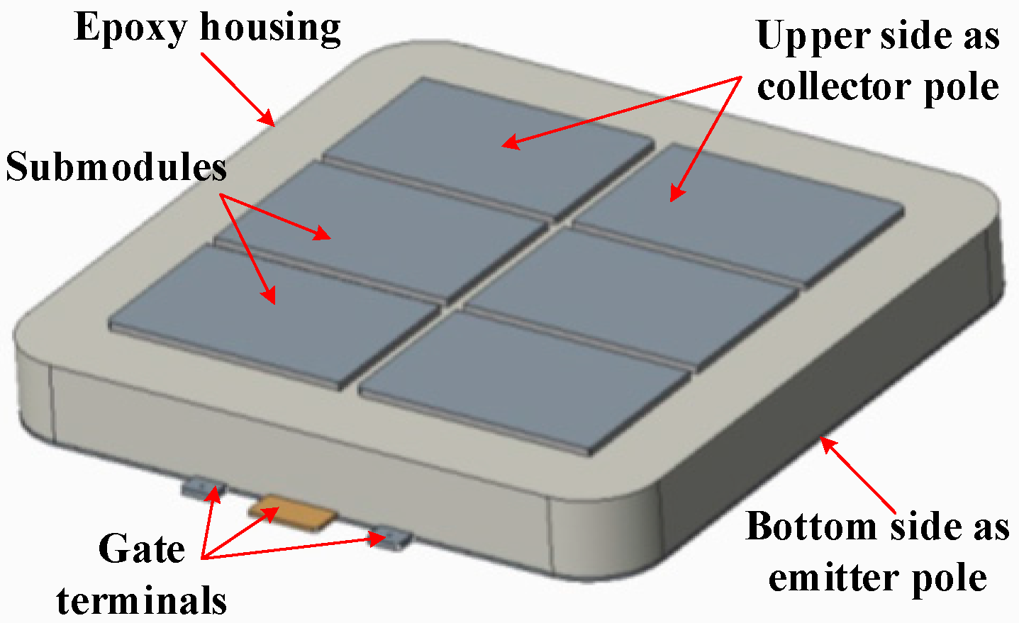
To elucidate the thermal performance for IGBT modules, the press-pack structure of power devices needs to be analyzed in detail. Without loss of generality, the StakPak press-pack IGBT rated at 4.5 kV and 3 kA (5SNA 3000K452300, ABB, Zurich, Switzerland) is chosen as the target device. The appearance of the target device as given by the Creo is shown in Figure 1 [20]. From the external point of view, the StakPak IGBT module looks like a flat cuboid. It consists of six identical submodules in parallel with insulated epoxy housing surrounding them. The upper side of the press-pack IGBT modules which is made up of contact faces of the submodules in Figure 1 acts as the collector pole and the bottom side with only one whole face acts as the emitter pole. The gate terminals are placed at the front edge of the target module, which includes a connecting interface and two screw holes for mounting the gate driver.
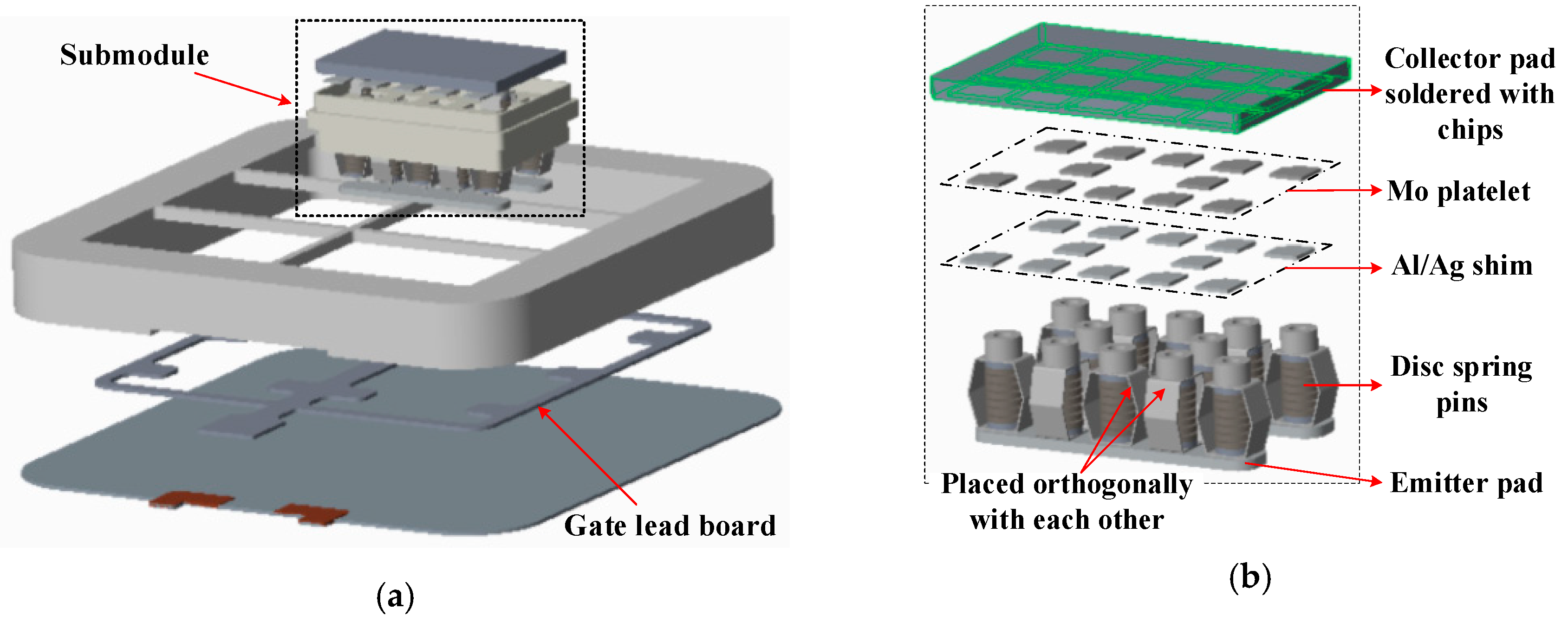
More in detail, the 3D model of StakPak press-pack IGBT is developed and the exploded graph which presents the internal profile of the IGBT module is displayed in Figure 2a. Thanks to the parallel and symmetrical configuration of submodules inside press-pack IGBT module shown in Figure 1, it is appropriate and time-saving to choose only one submodule in the dotted box to analyze the detailed profile shown in Figure 2b. The types of materials within the submodule are identified according to the information given by the IGBT module manufacturer. Since the epoxy housing frame is a kind of neat (unfilled) epoxy and provides a thermal conductivity of about 0.2 W/m·K. Meanwhile, and the typical thermal conductivity values of metals fall in the range of 50~300 W/m·K, it can be neglected when establishing the 3D model of press-pack IGBT since it is electrically and thermally isolated.
The highlighted part of the press-pack submodule in 
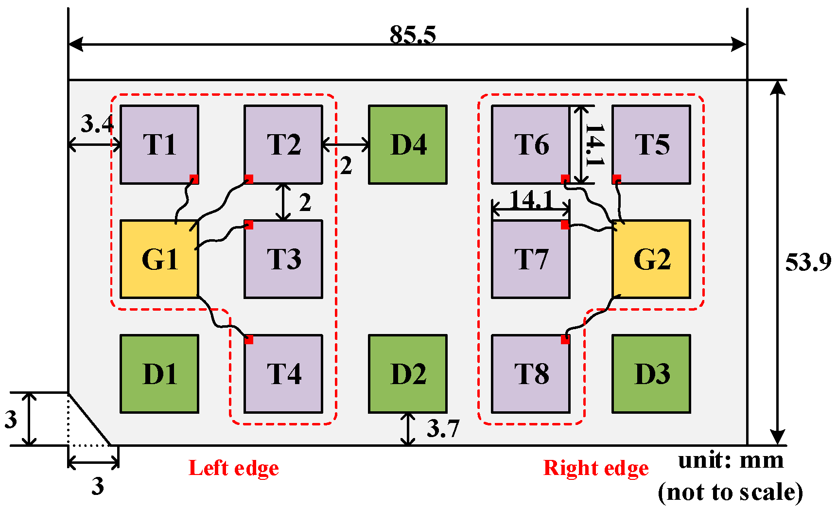
Figure 2b is the collector pad where the semiconductor chips are attached by soldering. The detailed layout of IGBT and free-wheeling diode (FWD) chips is configured, where the dimensions of and the distances between the chips are measured and displayed in Figure 3.
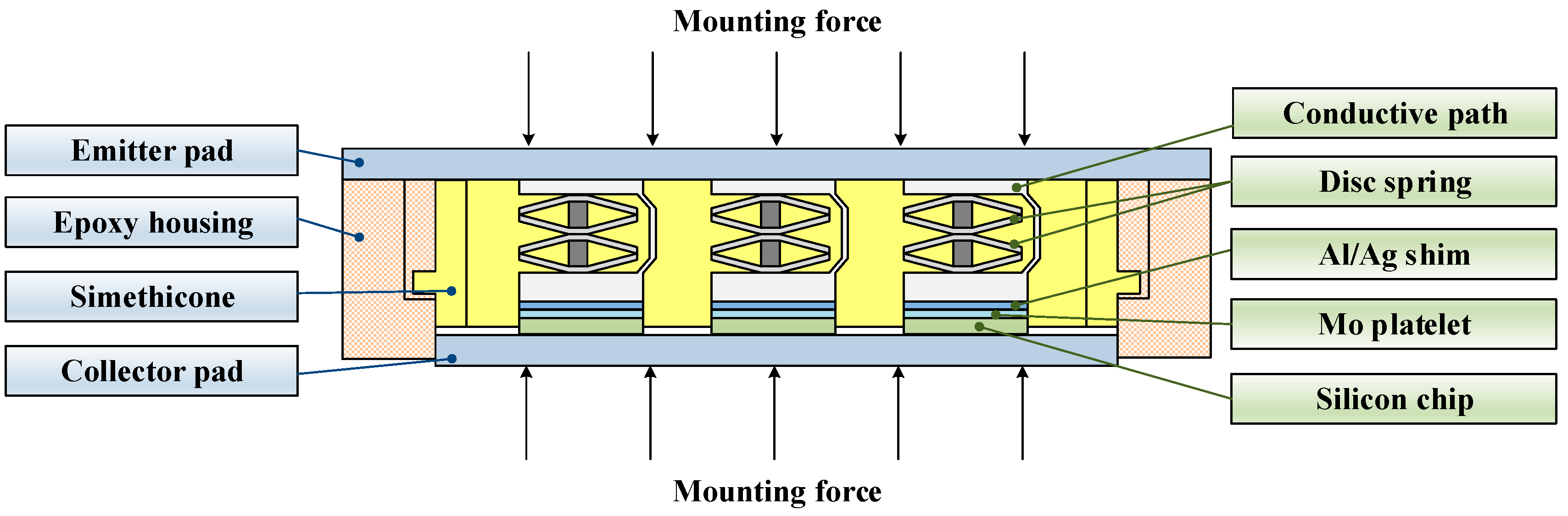
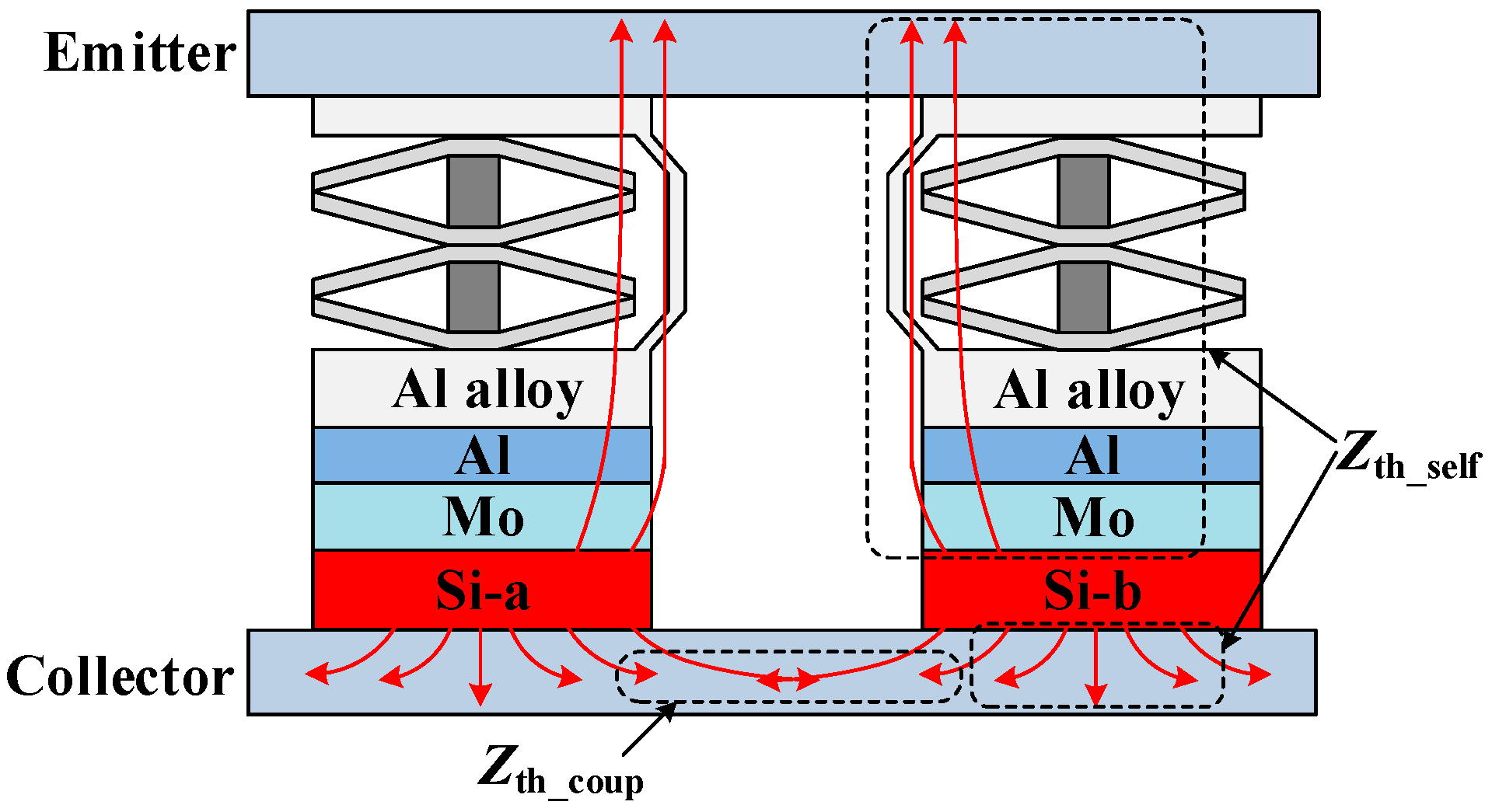
There are eight IGBT chips (marked as T), four FWD chips (marked as D) and two gate pads (marked as G) placed on the collector pad of the press-pack submodule in total. The IGBT chips share the same size as the FWD chips. Meanwhile, the gate pad at the left or right edge is linked up to four IGBT chips through silver wire. Since the distance between IGBT chips at the same edge and the gate pad is almost the same, it can be assumed that all four of the IGBT chips in parallel switch simultaneously as one group. Thus, the current sharing among the paralleled chips is balanced and the electrical stress of each chip is supposed to be equal. Based on the structural information analyzed above, the cross-sectional view of the internal structure of the submodule for press-pack IGBT device can be sketched as in Figure 4 to illustrate the heat flux and distribution of the target IGBT module.
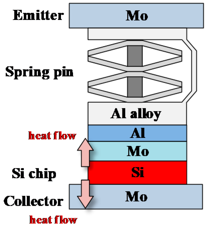
Two pads located on the upper plate or bottom plate play the role of conductive electrodes (i.e., collector and emitter poles), providing both the electrical and thermal paths for the semiconductor chips. Molybdenum plates of nearly the same size of IGBT chips or FWD chips directly soldered on the collector pad are placed in the middle of silicon chips and disc spring pins, which ensures the uniform distribution of the mounting force. Besides a silver or aluminum shim platelet is between the silicon chip and the Mo plate [12]. A semiconductor chip, an Al/Ag platelet and Mo plate form a chip assembly-like sandwiched structure. If the chip fails to short-circuit, the shim plate functions as a failure path to conduct the whole load current and then sufficiently high energy melts the platelet and forms a stable alloy with silicon [12].
Inside the press-pack IGBTs, the external clamping force is mounted to maintain the thermal contact of all layers and the part outside the disc spring pins acts as the conductive path connecting the collector pole and the emitter pole. It is assumed that every layer which conducts current is pressured tightly and connected without relative displacement and the silicon oil filling inside the module has small thermal conductivity and spread no heat, which confirms that all heat dissipates vertically from junction areas of the active chips to the cooling plates of both sides. As shown in Figure 2b, any two adjacent conductive paths outside the disc spring pins are placed orthogonally with each other, therefore it can be assumed that the layout of disc spring pins negligibly influences the thermal distribution vertically. The thermal conductivity of different packaging materials inside the studied press-pack IGBT module is obtained in [21,22] and listed in Table 1.

3. Impact of Press-Pack IGBT Double-Sided Structure on Thermal Distribution

As shown in Figure 4, the press-pack IGBT submodule consists of parallel chip assemblies which are made up of several press-contact layers. Among those, the single IGBT chip assembly is shown in 
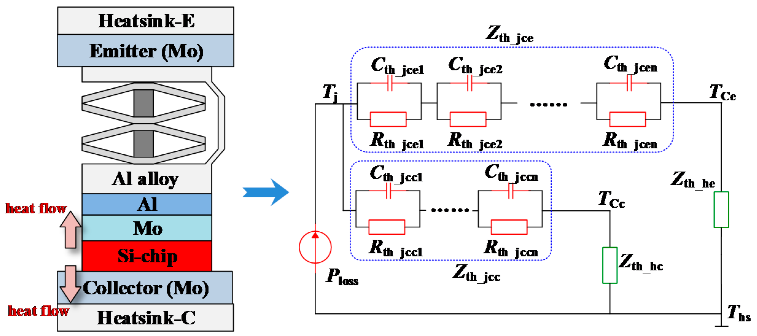
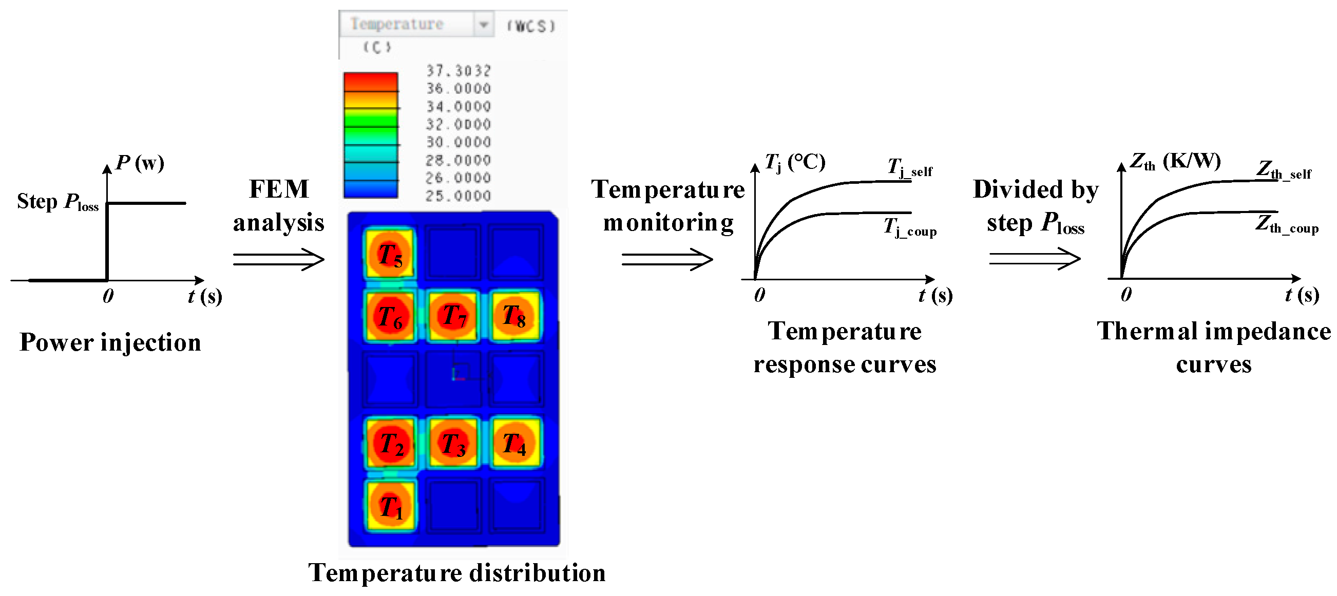
Figure 5. A temperature rise could be produced due to the self-heating of the active chip and the transient thermal impedance is gained. It is defined as Zth_jc as:
Z th _ jc = T j ( t ) T c ( t ) P loss = Δ T jc ( t ) P loss
where Tj(t) and Tc(t) are the temperatures of points located in the junction and case of the IGBT module, while ΔTjc is the temperature gap between the junction and case, Ploss is the power loss of the heating chip itself. The transient thermal impedance Zth_jc of the single chip assembly can be expressed as a lumped Foster-based RC thermal network model [23,24] based on thermal resistance Rth and thermal capacitance Cth of each layer.
It can be seen from 
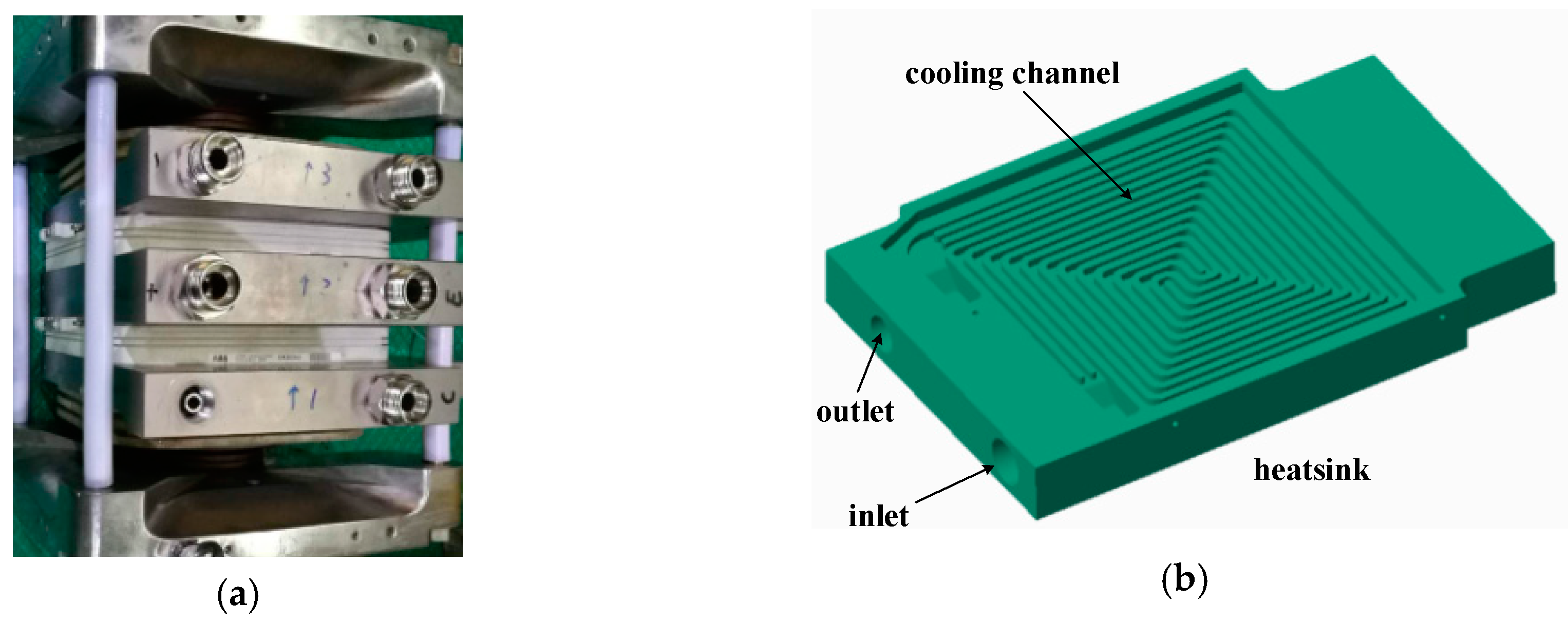
Figure 5 that the studied press-pack IGBT module features a double-sided cooling structure. Under double-sided cooling conditions, the heatsinks which are clamped on the surface of the heating press-pack module to achieve an effective cooling system act as both conducting and cooling components. A mechanical press-pack IGBT stack designed according to [25] configured as half bridge topology is shown in Figure 6a and the cooling channel inside the heatsink shown in Figure 6b is designed to allow the coolant to flow to the center first and then go out to the outlet. Through the cooling channel the heat is absorbed and the temperature spread on the heatsink surface is minimized as cold and hot water flows very close to each other.
To reduce the volume of the cooling pump, the cooling channels of heatsinks pressed together are often in series and thus lead to almost the same heat dissipation capability for every heatsink. In the cooling design for high power plastic IGBT modules, the heat dissipation parameters of heatsinks can be set as the same because plastic modules dissipate the heat by only one cooling side. However, the path of heat flow from press-pack chip junction to the collector cooling plate is shorter than that from the chip to the emitter cooling plate, which results in the difference of heat release between the two heatsinks pressed at the surface of press-pack IGBT module.
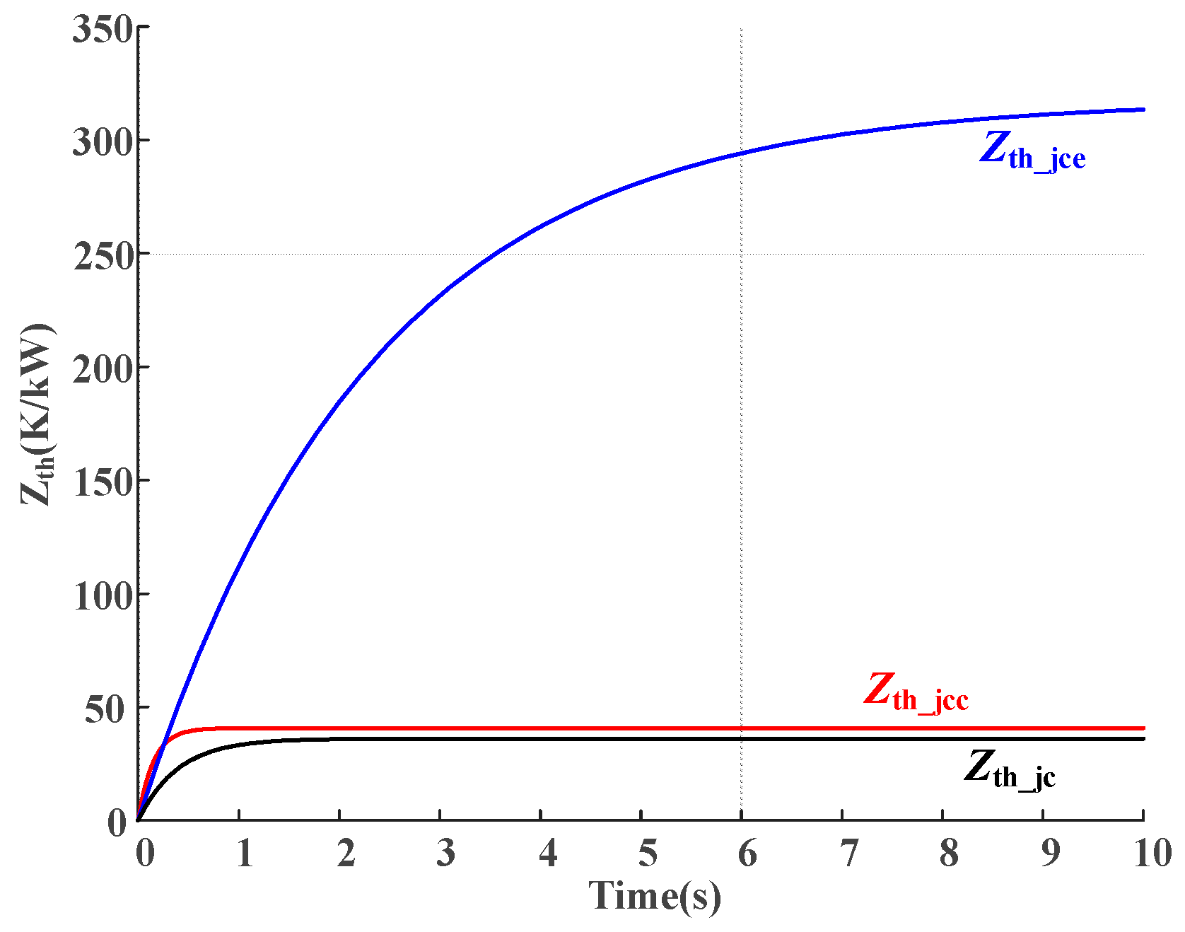
The equivalent thermal impedance of the single press-pack IGBT chip under double-sided cooling conditions is presented in Figure 7. The thermal parameters Zth_jcc and Zth_jce represent the thermal impedance from the chip junction to the collector surface and emitter surface. TCc and TCe is the case temperature of the collector case and emitter case. Zth_hc or Zth_he represents the thermal impedance of related heatsinks on either cooling side and they are supposed to have a very high heat transfer coefficient and very low thermal resistance in the boundary of the baseplate and the heatsink. Assume that the cooling conditions are kept the same (TCc=TCe) and thermal impedance Zth_jc from the junction of the semiconductor chip to the IGBT’s case is equal to Zth_jcc||Zth_jce.
To extract the thermal parameters of the press-pack IGBT module, the eight IGBT chips belonging to one submodule displayed in Figure 3 are picked out. As mentioned before, because the layout of chips and press-contact components is horizontally symmetrical, the analysis of thermal performance is concentrated on the chips of 1/2 unit (i.e., T1~T4) within the press-pack submodule in Figure 3. And since the conductive paths outside the disc springs are placed orthogonally, the paralleled coupling effects among conductive paths can be left out.

4. Matrix Thermal Modeling for Press-Pack IGBT

4.1. Matrix Thermal Network Model

The thermal impedance Zth_jc of Si chip only reflects the self-heating effect. However, the target StakPak module is featured by a multi-chip parallel structure. The thermal impedance Zth_jc can’t describe the thermal performance of the whole module in detail. Moreover, due to the fact the group of IGBT chips share the same collector baseplate shown in Figure 4, the existence of a multi-chip coupling effect is inevitable. Part of heat produced by chips is dissipated across the plate and this causes an increase in the temperature of the adjacent chip.
The heat flow path between coupled chips in parallel is shown in Figure 8, and the coupling thermal impedance Zth_c(a,b) between chip a and chip b can be written as Equation (2). In this way, the thermal coupling effect within the power module and the multi-chip coupling effect can be explored quantitively:
Z th _ c ( a , b ) ( t ) = T ja ( t ) T am ( t ) P coup _ b = Δ T th _ c ( a , b ) P coup _ b
where Tja(t) and Tam(t) represent the temperature in target points of chip a and ambient temperature, respectively, Pcoup_b is the power loss which is generated in the neighboring chip b. Because the chips share the same baseplate played as collector pad and the silicon oil filling in the IGBT module spreads little heat, the thermal coupling effect among the horizontal chips in the collector baseplate becomes the focus and the impact of disc spring pins on the thermal coupling effect vertically is reasonably neglected.
To establish a clear and effective thermal model for StakPak module, the thermal impedances that can not only reflect self-heating effect within one single chip but also represent the multi-chip coupling effect among different chips need to be obtained. To give a clear description for the complex thermal model, the mathematical tool – matrix is applied in this paper.
Combined with the self-heating thermal impedance Zth_self of the single chip and coupling thermal impedance Zth_c(a,b) between any neighboring chips, the mathematical tool – thermal impedance matrix including self-heating effect and multi-chip coupling is adopted as:
Z th _ jc = Z th _ self + Z th _ coup = [ Z th _ jc 1 0 0 0 Z th _ jc 2 0 0 0 Z th _ jcn ] + [ 0 Z th _ c ( 1 , 2 ) Z th _ c ( 1 , n ) Z th _ c ( 2 , 1 ) 0 Z th _ c ( 2 , n ) Z th _ c ( n , 1 ) Z th _ c ( n , 2 ) 0 ]
where diagonal elements represent self-thermal impedances of every heating chip, whereas off-diagonal elements are mutual thermal impedances which denote the thermal coupling effect. Employing the matrix method, the set of the junction temperature of the silicon chips can be calculated as:
[ T j 1 T j 2 T jn ] = [ Z th _ jc 1 Z th _ c ( 1 , 2 ) Z th _ c ( 1 , n ) Z th _ c ( 2 , 1 ) Z th _ jc 2 Z th _ c ( 2 , n ) Z th _ c ( n , 1 ) Z th _ c ( n , 2 ) Z th _ jcn ] [ P loss 1 P loss 2 P lossn ] + [ T hs T hs T hs ]
The thermal impedance matrix can be employed as a unified and accurate mathematical tool to analyse the thermal behaviour of high-power devices which use multi-chip design to increase the rated current.
Despite the thermal impedance matrix built for customized StakPak modules in Figure 3, the matrix method will be also effective if the distance between neighbouring chips is close enough and the thermal coupling effect is obvious. In [15], the study on thermal coupling effect is excellent but the IGBT module uses single-sided cooling conditions and the three-dimensional thermal distribution has not been established and can’t fit the thermal model of press-pack IGBT modules. Reference [18] has provided an overall introduction to the design and test of the press-pack IEGT based MMC-HVDC systems, but the multi-chip layout inside the Toshiba press-pack IEGT is viewed as a whole module and the thermal coupling effect has not been taken into account for thermal analysis. Hence, the proposed thermal matrix method will give a more detailed and accurate model for press-pack IGBT module with multi-chip layout and three-dimensional thermal distribution.

4.2. Elements Extraction in the Matrix Thermal Network Model

To extract the elements of the thermal impedance matrix in Equation (4), the Finite Element Method (FEM) is employed to obtain the temperature values affected by chip coupling with the established 3D model of the press-pack IGBT device illustrated in Figure 2.
From the electrical point of view, Zth_jc(t) functions as a step excitation response with a zero-initial condition. To make the extraction procedure convenient and ensure the accuracy at the same time, a first-order exponential formulation is adopted to express the transient thermal impedance and the thermal parameters can be expressed as the exponential terms:
Z th _ jc ( t ) = R th _ jc ( 1 e t / τ th _ jc ) , ( τ th _ jc = R th _ jc C th _ jc )
where τth_i is the time constant. It is worth noting that the thermal parameters of Rth and Cth just have mathematical meanings and the node voltages of the Foster-based RC network do not correspond to any real physical parameters. The order of RC components is related to the accuracy of numerical approximation instead of the number of packaging layers in the press-pack IGBT to curve-fit thermal impedance with adequate accuracy [24].
The extraction procedure is illustrated in Figure 9. By FEM simulation, a step power loss Ploss is loaded into a silicon chip (IGBT chip or diode chip) as the source of the simulation program. This assumed step power loss in Figure 9 only has mathematical meaning and does not have to correspond to a practical value because the thermal properties are not related to electrical parameters. Then the dynamic temperature response curves are scanned by monitoring some certain points located on the chips. Lastly, by dividing the temperature difference between the two adjacent regions (e.g., ΔTjc, ΔTth_c(a,b)) by the injected step power loss, the transient thermal impedance curves are obtained. In this way, the thermal impedance matrix for half of the press-pack submodule IGBT chips can be acquired with the results listed in Table 2.
In theory, the thermal coupling impedances between two chips should be the same despite the fact the coordinate (a, b) is reversed, however, there is still a little difference in the results of Table 2. That may be introduced by the estimation values extracted from FEM results but it has a slight influence on the thermal network model. The results listed in Table 2 show that the coupling thermal resistance decays when the distance of chips increases yet there is a sharp increment of the coupling thermal capacitance along with the longer distance. If the distance exceeds more than 10 mm, the thermal resistance drops to nearly zero and the thermal capacitance grows to the infinity which indicates that the coupling effect does not need to be considered.

4.3. Thermal Impedance Distribution on the Two Cooling Interfaces

Because the four IGBT chips (T1~T4) are in parallel within the press-pack IGBT submodule shown in Figure 3 and the thermal coupling effect between the chosen IGBT chip group and the others is not considered because the distance between the chosen group (T1~T4) and others is far. The extraction process mentioned in Figure 9 can be applied for the chip group to obtain the thermal impedance Zth_jcc and Zth_jce on the two cooling interfaces respectively as Equation (6). To simplify the fitting process, the order of the thermal network is set as 1:
Z th _ jcc ( t ) = 0.041 K / W × ( 1 e t / 0.15 sec ) Z th _ jce ( t ) = 0.32 K / W × ( 1 e t / 2.3 sec )
Applying Laplace transform, Zth_jc can be calculated as:
Z th _ jc ( s ) = Z th _ jcc ( s ) Z th _ jce ( s ) Z th _ jcc ( s ) + Z th _ jce ( s )
After inverse Laplace transform, Zth_jc yields:
Z th _ jc ( t ) = 0.038 K / W × ( 1 e t / 0.4 sec )
According to the datasheet of target IGBT module provided by the manufacturer [20], the thermal parameters of the four IGBT chips under double-sided cooling condition are calculated and listed in Table 3. The thermal impedance curves between the self-thermal impedance extraction by FEM and parameters listed in Table 3 are compared in Figure 10.
The comparison results plotted in Figure 10 shows that the FEM extraction results are a good approximation of the thermal parameters from the datasheet. Both curves demonstrate that steady state thermal impedances from the junction to both cooling cases of the single chip rises to about 38 K/kW and it takes nearly 2.5 s for the curves to enter the steady state. The distinction between them is the early transient behavior and the rising rate of extraction results from FEM is a little slower than the results provided by the datasheet. The reason is likely to be the simplification of the Foster-based thermal network with one RC ring during the thermal impedance extraction process. Nevertheless the extraction results are adequate to evaluate the thermal impedance’s distribution of the target press-pack IGBT.
The calculation results in Equation (6) imply that different heat propagation is undertaken between the collector side and the emitter side. The time constant of the junction to the collector’s case τth_jcc = 0.15 s and is much less than that of the junction to the emitter’s case τth_jcc = 2.3 s because of the unbalanced structure. Moreover, the thermal resistances Rth_jcc and Rth_jce are 0.041 K/W and 0.32 K/W respectively. The thermal impedance curves of Zth_jcc, Zth_jce, and Zth_jc are presented in Figure 11.
It can be calculated that when double-sided cooling is applied, about 88% of the chip’s power loss is conveyed through the path to the collector pad and the rest flows to the emitter pad. It suggests that a more sophisticated thermal management considering thermal stress distribution should be considered when designing the cooling plates mounting on the dual sides of StakPak IGBT modules. It should be noted that when the operating condition changes the thermal distribution of the two cooling sides will not change too much. Because the thermal model is built based on material thermal properties such as the thermal conductivity and mass density that are inherent attributes of the materials themselves and are not related to the operating condition like DC voltage or load current. Even the temperature factor has been considered when establishing the model. The thermal path is mainly composed of metals and it can be found in Table 1 that the thermal conductivity of metals differs slightly when temperature changes, so the thermal impedance curves can be applied even when the operating conditions change.

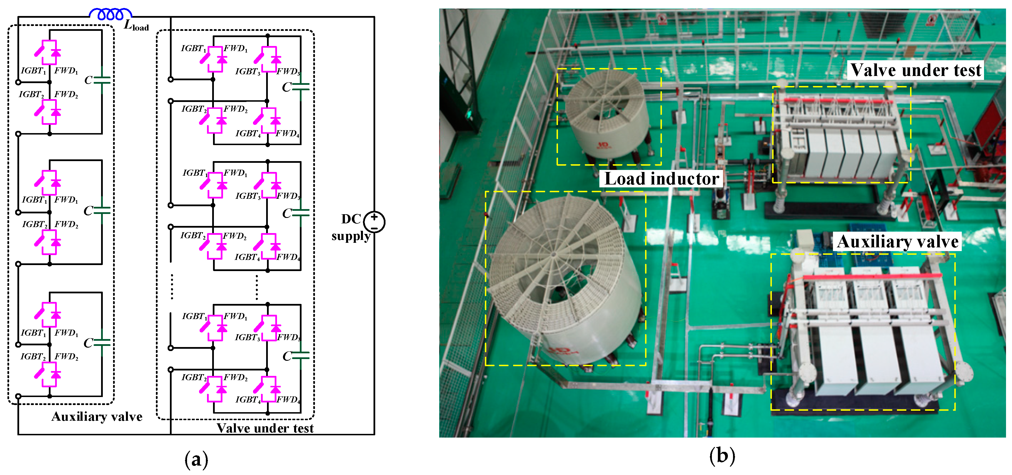
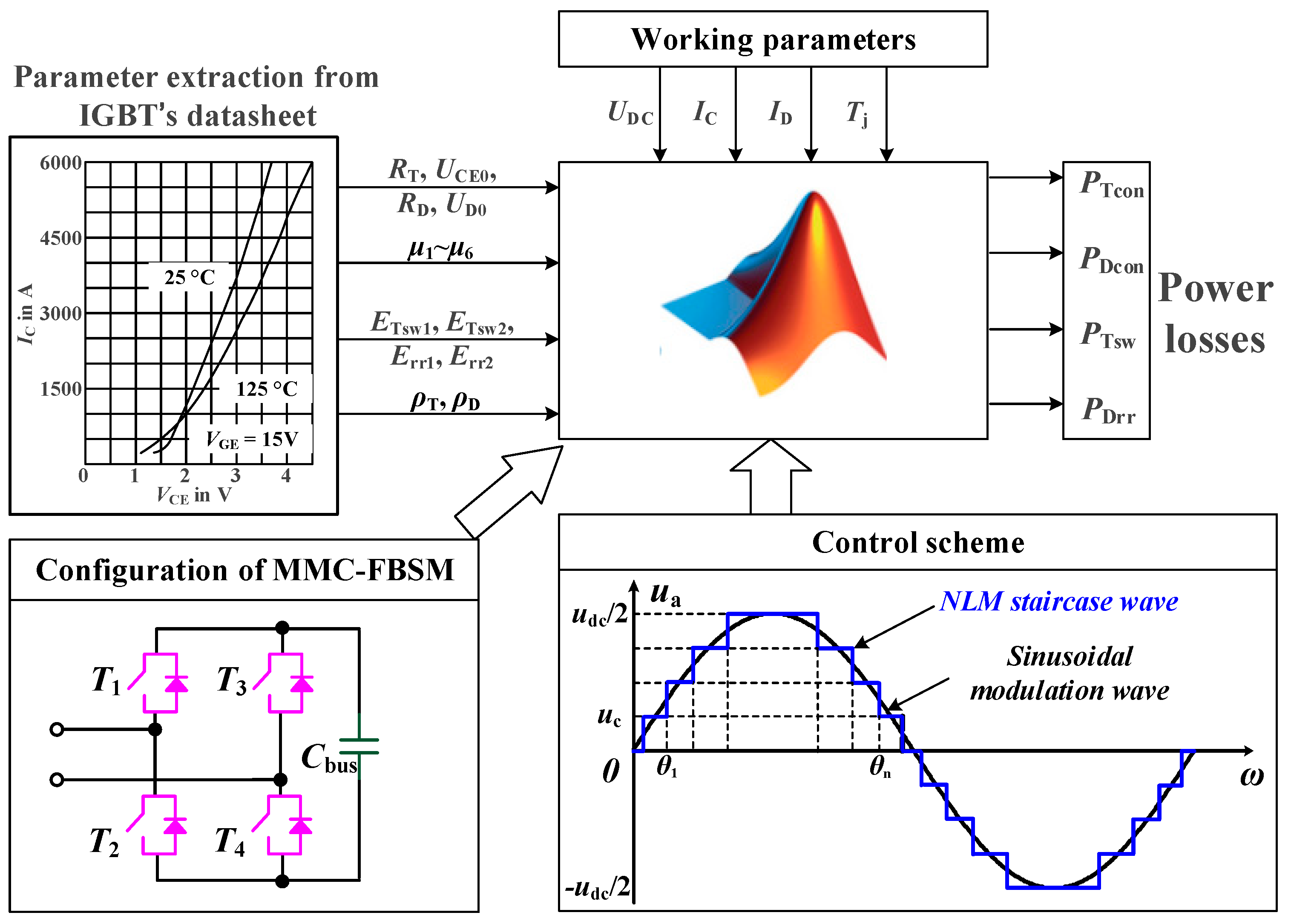
5. Model Verification

In this section, the target press-pack IGBT module is employed in the electrical type test setup of modular-multilevel-converter based high-voltage-direct-current (MMC-HVDC) [26] and the schematic diagram of the converter is shown in Figure 12a. Due to the unbalanced thermal distribution analyzed in Section 4, the unbalanced power loss distribution of the press-pack IGBT module in the MMC-HVDC power stack is considered and the thermal stress should be evaluated to ensure the reliable operation of MMC-HVDC system. Thus, the electrical type test setup of the MMC valves is established in Figure 12b and the valves under the test are made up of six full-bridge submodules (FBSMs) and the auxiliary valve is made up of three half-bridge submodules (HBSMs). The operation parameters of the test setup are listed in Table 4. The switching frequency listed in Table 4 is set to be about 150 Hz which is the same as that in [26].
To obtain the power loss of MMC converters, the MMC converter model configured as Figure 12a is built in Matlab and it is implemented with the strategy of nearest-level-modulation [27,28]. The power loss of IGBT module consists of IGBT’s power loss and free-wheeling diode’s (FWD’s) power loss. The IGBT’s power loss PT is made up of IGBT’s conduction loss PTcon and switching loss PTsw while FWD’s loss includes FWD’s conduction loss PDcon and reverse recovery loss PDrr, of which the conduction loss is expressed as Equation (9) [29]:
{ P T c o n = U C E I C = ( R T I C + U C E 0 ) I C P D c o n = U D I D = ( R D I D + U D 0 ) I D
In Equation (9) UCE and IC denote the collector-emitter voltage drop and the collector current of IGBT when it is on conduction stage, and RT and UCE0 mean the forward conduction resistance and the latch-up voltage of target IGBT which can be extracted from the curve of the on-state characteristics in [20]. Likewise, UD and ID are the forward voltage drop and the conduction current of FWD, and RD and UD0 represent the FWD’s conduction resistance and the latch-up voltage.
The switching loss of IGBT and FWD is shown in Equation (10) [29], where UDC stands for the DC-link voltage while Ts and Tm denote the switching period and modulation period. ETsw and Err are switching energy and reverse recovery energy of IGBT and FWD, respectively. The coefficients μ1~μ6 are temperature-dependent parameters which can be obtained by fitting curves of Esw-IC or Err-IC from [20]. Since μ1~μ6 are temperature-dependent, the temperature coefficients ρT and ρD are used to calculate the loss accurately under different temperature. ρT and ρD can be gotten by the interpolation method where Tj means junction temperature of IGBT module. ETsw1 and ETsw2 refer to the switching energy of IGBT under 125 °C and 25 °C, respectively. Similarly, Err1 and Err2 are used to represent the reverse recovery energy of FWD under 125 °C and 25 °C. All of the energy parameters are available in the manufacturer’s datasheet:
{ P T s w = 1 T s T m E T s w = 1 T s T m U D C ( μ 1 + μ 2 I C + μ 3 I C 2 ) ρ T P D r r = 1 T s T m E r r = 1 T s T m U D C ( μ 4 + μ 5 I C + μ 6 I C 2 ) ρ D ρ T = 1 E T s w 1 [ E T s w 1 E T s w 2 125 25 ( T j 25 ) + E T s w 2 ] ρ D = 1 E r r 1 [ E r r 1 E r r 2 125 25 ( T j 25 ) + E r r 2 ]
In this way, the data and parameters related to the module’s power loss from [20] are added to the simulation model. Based on the simulation model, the power losses’ calculation procedure is presented in Figure 13, and the results of power losses for the press-pack IGBT modules are listed in Table 5.
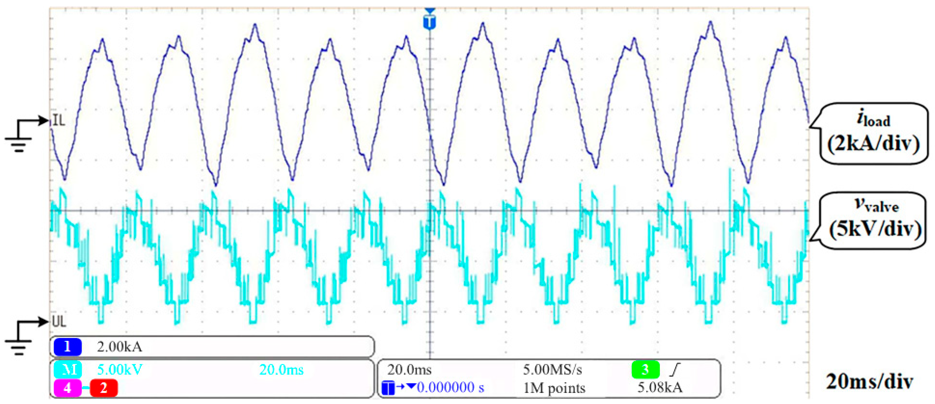
The total loss of average power losses in the IGBT modules is calculated as 17.42 kW. To validate the simulation results, the total average power loss of the FBSM should be acquired and the waveforms of the MMC valve under the required test parameters in Table 4 is measured in Figure 14.
The power loss of MMC valves is usually measured by means of a power analyzer. However, due to the high power rating of MMC type test setup, the cost of a proprietary power analyzer is unaffordable. Thus, the method of liquid calorimetry is developed and utilized to measure the average power loss of a single MMC-FBSM.
Since the heatsinks of the press-pack stack in Figure 6 are designed with water cooling structure, liquid calorimetry can be applied in the press-pack stack to measure the quantity of heat absorbed by the coolant. Thanks to the compact packaging assembly of the mechanical press-pack stack, the heat dissipation of power devices is almost absorbed by the heatsinks and the heat is calculated as Equation (11):
H = Q C ρ Δ t
where H is the heat absorbed by coolant and Δt is the temperature difference between the inlet and outlet of the heatsink. The volume flow rate is symbolized as Q, while C and ρ mean the specific heat capacity and density of the coolant. To measure the temperature difference Δ
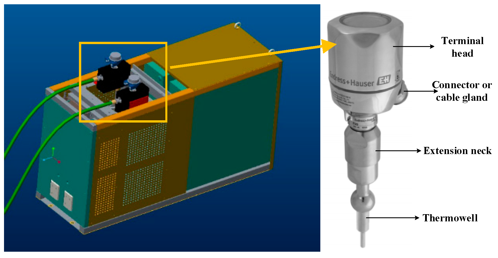
t, an iTHERM TM411 thermometer [30] is placed at the inlet and outlet of the heatsink and the configuration of the thermometer is shown in Figure 15.
Based on the thermometer and the cooling system, the average power loss of the single MMC-full-bridge-submodule (MMC-FBSM) can be obtained. The specific heat capacity and density of the coolant are 4200 J/(kg·K) and 1000 kg/m3. The volumetric flow rate of the cooling system is set to be 16.8 L/min. The temperature difference between the inlet and outlet measured by the thermometers is listed in Table 6.
The error between the simulation results and the measurement is around 5%, hence the calorimetry method usefulness is verified and thee average power loss distribution listed in Table 5 can be applied in the analysis for the thermal behavior of the press-pack IGBT modules.
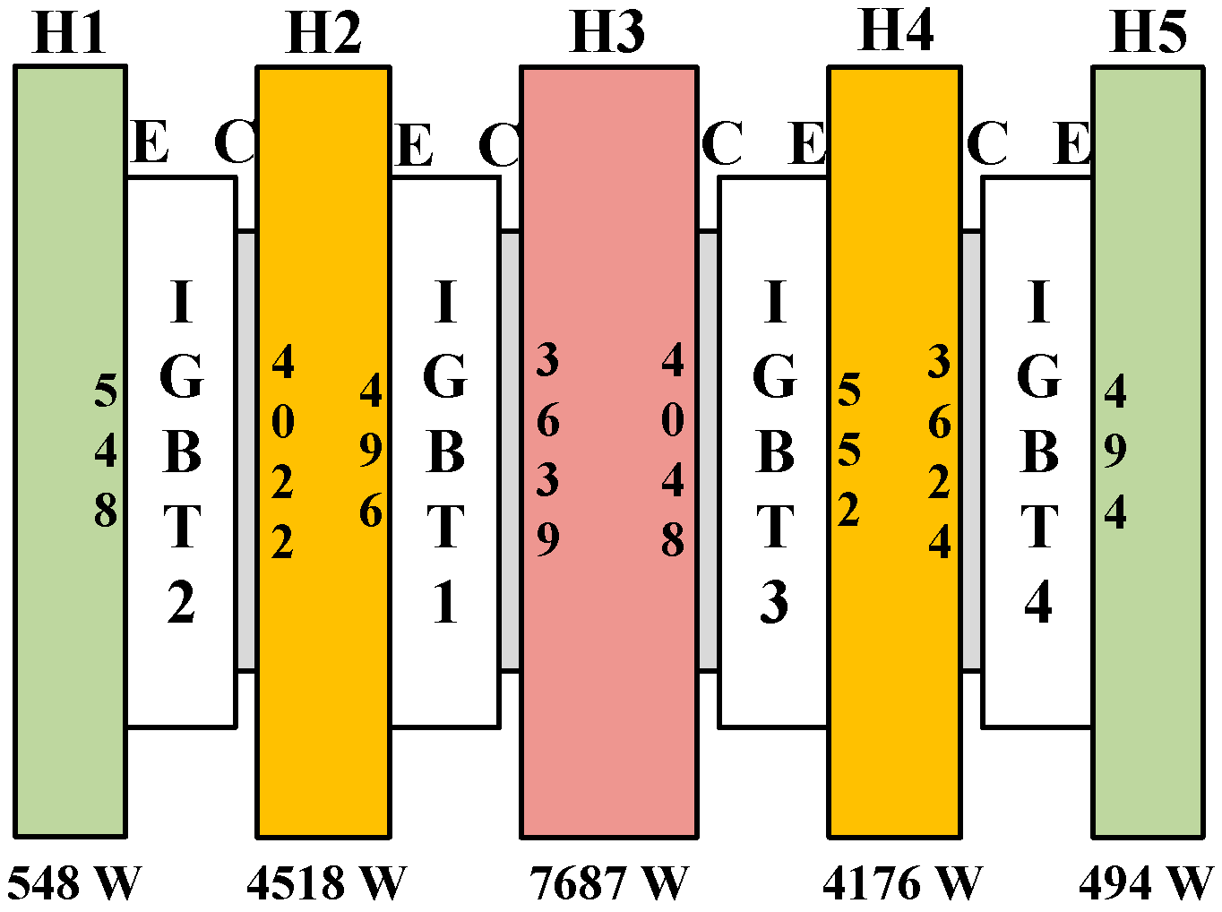
According to the loss distribution analysis of the press-pack IGBT module under double-sided cooling conditions which indicates that 88% of the module’s power loss is dissipated through the collector pad and the rest flows to the emitter pad, the loss distribution for the MMC-FBSM is calculated as illustrated in Figure 16. The heatsink H1 undertakes the part of power loss dissipated from the emitter side of IGBT2, while the heat stress for H2 is made up of the power loss from the emitter side of IGBT1 and collector side of IGBT2. The power loss of heatsink H1 and H5 is almost the same. And H2 and H4 share nearly the same thermal stress as well. The heatsink in the middle of the stack undertakes the most power loss which absorbs the part of power loss from the collector side of IGBT1 and IGBT3.
To verify the validation of the proposed thermal model in Section 4, the junction temperature of the critical points in the collector side of IGBT chip T2 in Figure 3 is calculated via the proposed matrix thermal model and the lumped RC thermal model of which the parameters are dependent on Table 3. The power loss injected to the proposed matrix thermal model is the distributed loss on the collector side of the press-pack IGBT while the loss as the input of traditional lumped RC model is the whole loss of the press-pack IGBT. The type of test setup in 
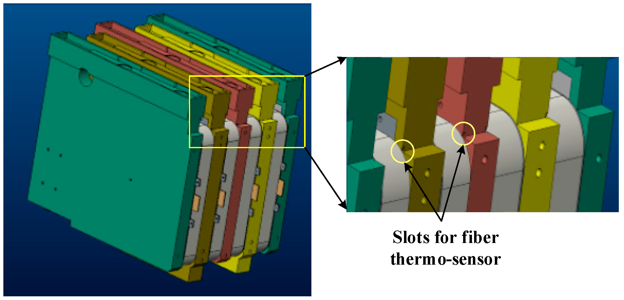
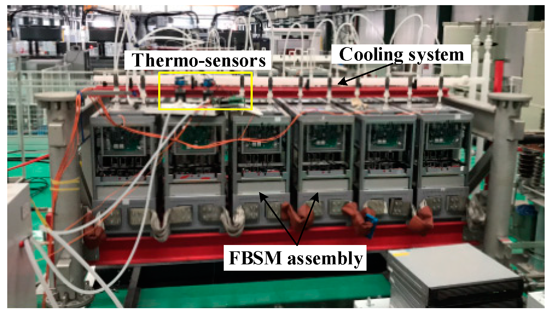
Figure 12 is employed, where the instant junction temperature is measured by optic fiber thermosensors. The optic fiber temperature sensor’s resolution is 0.1 °C which is enough to ensure the accuracy of the measurements. It is placed clinging to the press-pack IGBT’s submodule through the slot in the heatsink shown in Figure 17. Through the slot, the fiber can be placed right at the chip whose coupling effect is the most obvious. The test setup with the optic fiber thermosensors is displayed in Figure 18.
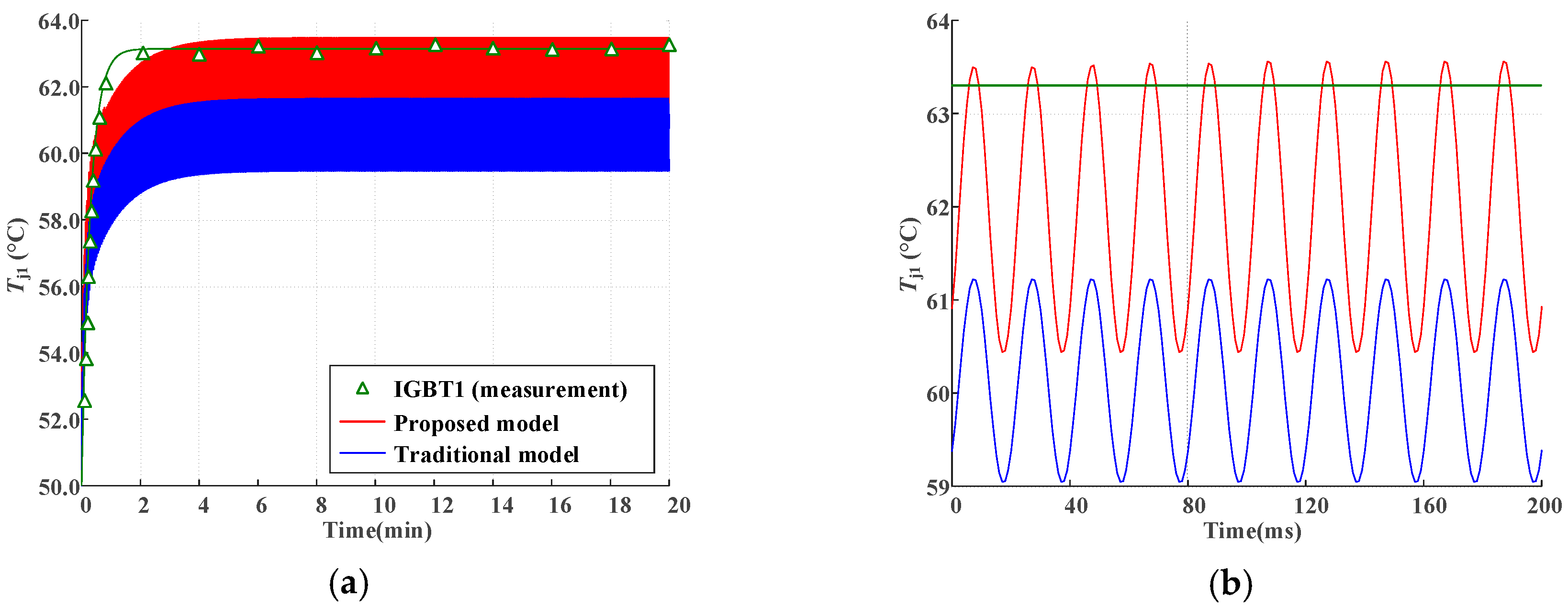
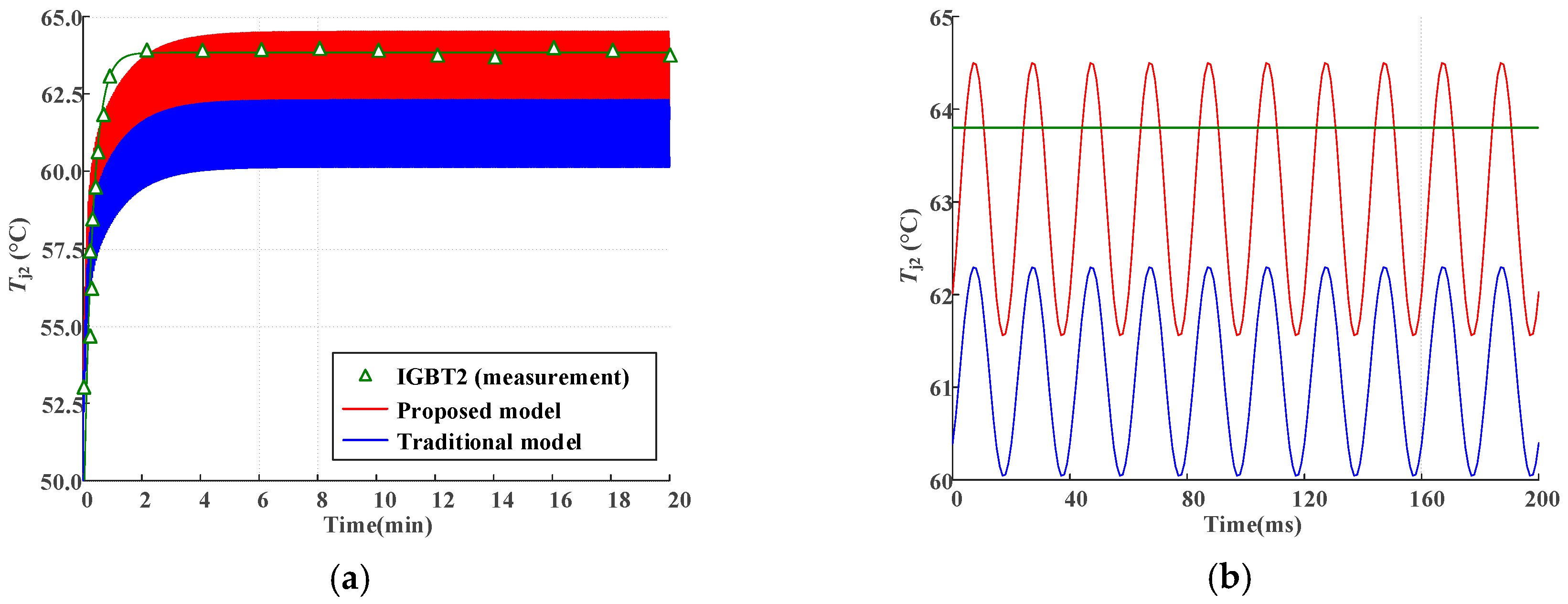
With the fiber thermosensors shown in Figure 19, the simulated junction temperature swings using the proposed model and the traditional lumped RC model of which the parameters supported by the manufacturer are presented in Figure 20 and Figure 21, respectively.
The results are compared with the test measurements. The temperature of the IGBT module is measured every 2 minutes, and before it reaches the steady state the temperature is recorded about every 10 seconds. The measurement value of the collector’s temperature is marked with a triangle. The fitting curves are compared with the simulation curve. Figure 20 displays the comparison between measurement results and model calculation for the junction temperature of IGBT1 which is marked by Tj1, meanwhile, the comparison for the junction temperature of IGBT2 which is denoted as Tj2 is shown in Figure 21. The junction temperature curves gotten by proposed method and conventional method in Figure 20 fall to range of 60.5 °C~63.4 °C and 59 °C~61.2 °C, while in Figure 21 the curves fall to range of 61.6 °C~64.5 °C and 60 °C~62.3 °C. From the two figures it can be observed that the gap between the average simulation results of the proposed thermal model and the measurements is about 1.5 °C in Tj1 and 1.0 °C in Tj2, respectively, but the difference between the average simulation results of traditional thermal model and the measurements is about 3.4 °C in Tj1 and 3.6 °C in Tj2, respectively. The junction temperature of Tj1 is about 0.5 °C lower than Tj2 which corresponds to the higher power loss of Tj2. The error between the measurements and the simulation results of the proposed thermal model is less than 2.1% while that between the measurements and the simulation results of traditional thermal model is about 5.5%. The differences between experimental results and calculation results by conventional and proposed methods are displayed in
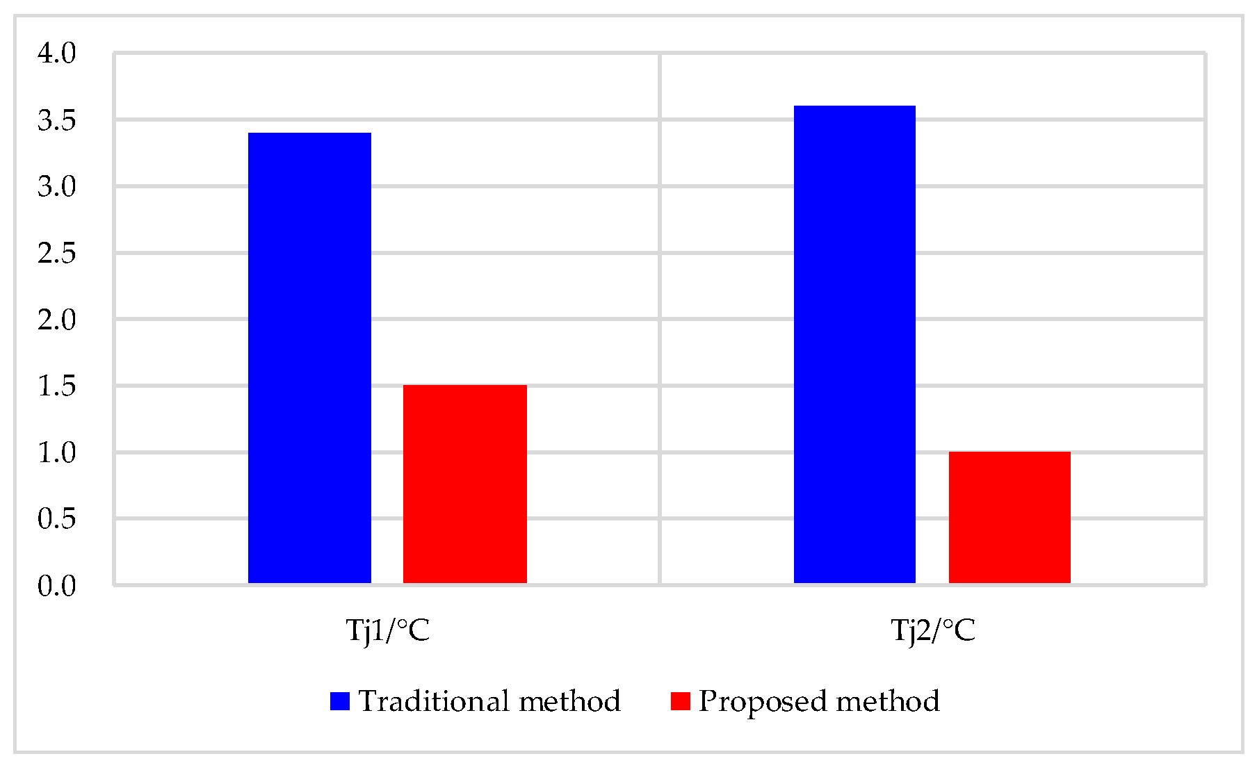
 Figure 22.
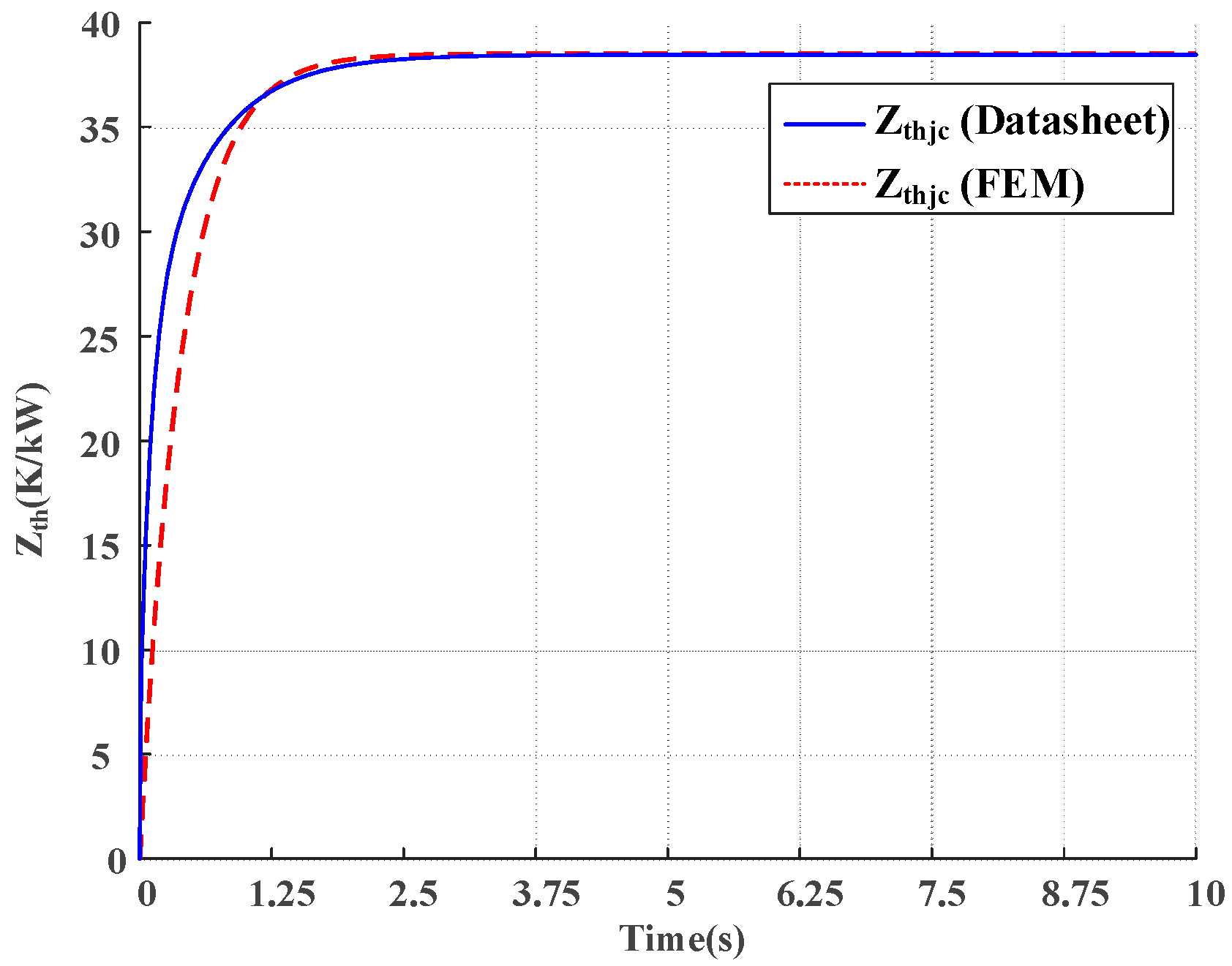
It can be verified that the matrix thermal model of the press-pack IGBT module under double-sided cooling conditions more closely fits the practical thermal behavior of the target module than the traditional RC model. The error between the proposed model and the traditional model will increase if the power loss generated by the IGBT module increases, and the thermal distribution could be more unbalanced if the operating conditions change. The proposed thermal model has considered the multi-chip thermal coupling effect and the thermal distribution between the two cooling plates inside the press-pack IGBT module. It does not only allow the accurate evaluation of the junction temperature of the press-pack IGBT module, but also helps to improve the cooling capability of the heat exchanger and reconstruct the thermal management in high power converter systems such as the MMC-HVDC system based on press-pack IGBT modules.

6. Conclusions

Despite the fact press-pack IGBT modules are being paid more and more attention in high power applications such as MMC-HVDC systems, studies on their accurate thermal performance and thermal management models are limited. Moreover, the intrusive junction temperature extraction method is not easy to employ because of compact and hermetic package design of press-pack IGBT modules. In this paper, the comprehensive chip-level thermal distribution model of the StakPak press-pack IGBT under the double-sided cooling condition is analyzed. Besides, the thermal network matrix considering the internal multi-chip effect is also obtained to explore how the thermal behavior of the StakPak module is affected by the multi-chip press-pack layout.
Owing to the fact the unbalanced pressure-contact layers are structured vertically, the thermal impedance of junction to the collector cooling case is different from that of the emitter case. Based on the analysis of the internal structure of a StakPak IGBT (5SNA 3000K452300), an accurate thermal network matrix integrated with thermal coupling impedance is introduced. Simulation verifications have shown that the proposed model is in good agreement with the thermal parameters provided by the manufacturer. Besides, it is derived that about 88% of the power losses from the active chip flow to the collector surface and the rest flows to the emitter surface of the press-pack IGBT. To verify the thermal stress of the studied module, the StakPak IGBTs are employed in the electrical type test setup for the application of MMC-HVDC. The proposed thermal network model is utilized to calculate the junction temperature and the results obtained are compared with the measurements. The verification shows that the proposed thermal network model for the press-pack IGBT module presents satisfactory performance in terms of average junction temperature measurement.
Conventional power devices are characterized by single-sided cooling and studies on thermal performance for power devices with double-sided cooling structure are few. In general, little attention has been paid to the thermal distribution on the cooling sides and often the thermal dissipation capabilities of the two cooling sides are viewed as the same. This paper has dissected the chip-level structure of press-pack based StakPak modules and the thermal stress distribution of the two cooling sides quantitively. What’s more, the effect of thermal coupling effect between neighboring chips on the thermal behavior of the power devices has also been analyzed and hot spots will be produced and more efficient cooling designs are needed. With proposed thermal network model, targeted and efficient cooling design will be implemented in MMC submodules to decrease the thermal stresses. The operation reliability can be improved and maintenance cost of MMC-HVDC systems can be reduced. The future work will be focused on the specifically designed heatsink for StakPak devices in the MMC-FBSM and the thermal stresses can be compared with the conventional ones to verify the feasibility and availability of improved thermal management.

Author Contributions

Y.C., H.L., W.L. (Wuhua Li), X.H. had developed the originally proposed modeling work. Y.C., W.L. (Weixing Lin) had implemented with MMC-HVDC type test setup system for investigation and performance validation. F.I. and F.B. contributed his expertise in the proposed subject of research and verification of the obtained results based on theoretical concepts and insight background. All authors involved to articulate the research work for its final depiction as the research paper.

Funding

This work is sponsored by the National Key Research and Development Program of China (2017YFE0112400), the National Nature Science Foundations of China (U1834205, 51677166) and the Zhejiang Provincial Key Research and Development Program (2018C01SA150059).

Conflicts of Interest

The authors declare no conflict of interest.

Nomenclature

TjJunction temperature of IGBT
TcCase temperature of IGBT
ΔTjcTemperature gap between junction and case
PlossPower loss of the heating chip
Zth_jcThermal impedance from the chip junction to the module’s case
Zth_jcc/Zth_jceThermal impedance from the chip junction to the collector/emitter surface
TCc/TCeCase temperature of the collector/emitter case
Zth_hc/Zth_heThermal impedance from the heatsink to the collector/emitter cooling side
TjaJunction temperature in target points of chip a
TamAmbient temperature
THTemperature of heatsink in the MMC full-bridge submodule
Pcoup_bPower loss generated in the neighbor chip b
Zth_c(a,b)Coupling thermal impedance between chip a and chip b
Zth_selfSelf-heating thermal impedance
Zth_coupCoupling thermal impedance
Rth_jcThermal resistance from the chip junction to the case
Rth_jcc/Rth_jceThermal resistance from the chip junction to the collector/emitter’s case
Cth_jcThermal capacitance from the chip junction to the case
τth_jcTime constant of thermal impedance
τth_jcc/τth_jceTime constant of the chip junction to the collector/emitter’s case

References

  1. Yoshikazu, T.; Koh, Y.; Masayuki, S.; Takeshi, F.; Humiaki, K.; Yasukazu, S. 2.5 kV-1000 A power pack IGBT (high power flat-packaged NPT type RC-IGBT). IEEE Trans. Electron Devices 1999, 30, 245–250. [Google Scholar]
  2. Cristian, B.; Remus, T.; Frede, B.; Stig, M.N.; Lars, H.; Tusitha, A.; Pedro, R. An overview of the reliability prediction related aspects of high power IGBTs in wind power applications. Microelectron. Reliab. 2011, 51, 1903–1907. [Google Scholar] [Green Version]
  3. Yang, L.; Yahui, L.; Guoqing, L.; Dongbo, Z.; Chen, C. Two-stage multi-objective OPF for AC/DC grids with VSC-HVDC: Incorporating decisions analysis into optimization process. Energy 2018, 147, 286–296. [Google Scholar]
  4. Robin, S.; Ashley, P.; Michael, V.; Charles, T.; Paul, T.; Xiaoping, D. Press-pack IGBTs for HVDC and FACTs. CSEE J. Power Energy Syst. 2017, 3, 302–310. [Google Scholar]
  5. Mohamed, A.; Ehab, E.-S. Power Sharing Control Strategy of Multiterminal VSC-HVDC Transmission Systems Utilizing Adaptive Voltage Droop. IEEE Trans. Sustain. Energy 2017, 8, 605–615. [Google Scholar]
  6. Paolo, C.; Gianni, N.; Alessandro, P.; Marco, P.; Maurizio, P. Power cycling on press-pack IGBTs: Measurements and thermomechanical simulation. Microelectron. Reliab. 1999, 39, 1165–1170. [Google Scholar]
  7. Allen, R.H.; David, L.B. Simulating the dynamic electrothermal behavior of power electronic circuits and systems. IEEE Trans. Power Electron. 1993, 8, 376–385. [Google Scholar]
  8. Homer, A.M.; Allen, R.H. Electrothermal simulation of an IGBT PWM inverter. IEEE Trans. Power Electron. 1997, 12, 474–484. [Google Scholar]
  9. Petar, M.I.; Phil, A.M.; Malcolm, S.T.; Stephen, B. Dynamic Electro-Thermal Physically Based Compact Models of the Power Devices for Device and Circuit Simulations. In Proceedings of the Annual IEEE Semiconductor Thermal Measurement and Management Symposium (Cat. No.01CH37189), San Jose, CA, USA, 22 March 2001; pp. 35–42. [Google Scholar]
  10. Chan-Su, Y.; Paolo, M.; Mauro, C.; Wolfgang, F. Thermal component model for electrothermal analysis of IGBT module systems. IEEE Trans. Adv. Packag. 2001, 24, 401–406. [Google Scholar] [CrossRef]
  11. IEGT (PPI & PMI). Available online: https://toshiba.semicon-storage.com/ap-en/product/bipolar-transistor/iegt.html (accessed on 14 November 2018).
  12. Simon, E.; Munaf, R.; Evgeny, T.; Daniel, S.; Arnost, K.; Ulrich, S.; Eric, C. 4.5kV Press Pack IGBT Designed for Ruggedness and Reliability. In Proceedings of the Conference Record of the 2004 IEEE Industry Applications Conference, 2004. 39th IAS Annual Meeting, Seattle, WA, USA, 3–7 October 2004; pp. 1534–1539. [Google Scholar]
  13. Amir, S.B.; Ke, M.; Frede, B. Thermal Impedance Model of High Power IGBT Modules Considering Heat Coupling Effects. In Proceedings of the 2014 International Power Electronics and Application Conference and Exposition, Shanghai, China, 5–8 November 2014; pp. 1382–1387. [Google Scholar]
  14. Ming, C.; An, H.; Xidang, Y. Predicting IGBT Junction Temperature with Thermal Network Component Model. In Proceedings of the 2011 Asia-Pacific Power and Energy Engineering Conference, Wuhan, China, 25–28 March 2011; pp. 1–4. [Google Scholar]
  15. Amir, S.B.; Ke, M.; Frede, B. A Lumped Thermal Model Including Thermal Coupling and Thermal Boundary Conditions for High-Power IGBT Modules. IEEE Trans. Power Electron. 2018, 33, 2518–2530. [Google Scholar] [Green Version]
  16. Amir, S.B.; Ke, M.; Pramod, G.; Francesco, I.; Frede, B. A 3-D-Lumped Thermal Network Model for Long-Term Load Profiles Analysis in High-Power IGBT Modules. IEEE J. Emerg. Sel. Top. Power Electron. 2016, 4, 1050–1063. [Google Scholar]
  17. Merouane, O.; Zoubir, K.; Ali, I.; Jean, P.O.; Radoslava, M.; Miaoxin, W. New Analytical Model for Real-Time Junction Temperature Estimation of Multichip Power Module Used in a Motor Drive. IEEE Trans. Power Electron. 2018, 33, 5292–5301. [Google Scholar]
  18. Huifeng, C.; Wenping, C.; Paolo, B.; Rong, Y.; Haitao, Z.; Wei, S. Design and Testing of the World’s First Single-Level Press-Pack IGBT Based Submodule for MMC VSC HVDC Applications. In Proceedings of the 2015 IEEE Energy Conversion Congress and Exposition (ECCE), Montreal, QC, Canada, 20–24 September 2015; pp. 3359–3366. [Google Scholar]
  19. Erping, D.; Zhibin, Z.; Peng, Z.; Jinyuan, L.; Yongzhang, H. Study on the Method to Measure the Junction-to-Case Thermal Resistance of Press-Pack IGBTs. IEEE Trans. Power Electron. 2018, 33, 4352–4361. [Google Scholar]
  20. 5SNA 3000K452300 StakPak IGBT Module Datasheet; ABB Switzerland Ltd.: Lenzburg, Switzerland, 2016.
  21. Andreas, V.; Michael, H. Materials and Their Thermal Properties in IGBT Modules: Technologies, Driver and Application, 2nd ed.; Infineon: Neubiberg, Germany, 2012; pp. 173–175. [Google Scholar]
  22. Zehringer, R.; Stuck, A.; Thomas, L. Material requirements for high voltage, high power IGBT devices. Solid-State Electron. 1998, 42, 2139–2151. [Google Scholar] [CrossRef]
  23. Shan, Y.; Tao, W.; King, J.T.; Jiyun, Z.; Xiaolei, H. Electro-Thermal Modeling of SiC Power Devices for Circuit Simulation. In Proceedings of the 39th Annual Conference of the IEEE Industrial Electronics Society, Vienna, Austria, 10–13 November 2013; pp. 718–723. [Google Scholar]
  24. Zhaohui, L.; Hyungkeun, A.; Mahmoud, A.E.N. A thermal model for insulated gate bipolar transistor module. IEEE Trans. Power Electron. 2004, 19, 902–907. [Google Scholar]
  25. Backlund, B.; Schweizer, T. Recommendations Regarding Mechanical Clamping of Press-Pack High. Power Semiconductors; ABB Switzerland Ltd.: Lenzburg, Switzerland, 2006. [Google Scholar]
  26. Tianning, X.; Phil, S.J.; Colin, C.D. Electrical type tests for the voltage sourced converter valves based on modular multi-level converter. In Proceedings of the 17th European Conference on Power Electronics and Applications (EPE’15 ECCE-Europe), Geneva, Switzerland, 8–10 September 2015; pp. 1–10. [Google Scholar]
  27. Miguel, M.; Emilio, J.B.; Francisco, J.R.; Inés, S. Implementation of Nearest Level Modulation for Modular Multilevel Converter. In Proceedings of the 2015 IEEE 6th International Symposium on Power Electronics for Distributed Generation Systems (PEDG), Aachen, Germany, 22–25 June 2015; pp. 1–5. [Google Scholar]
  28. Minyuan, G.; Zheng, X.; Qingrui, T.; Weiyong, P. Nearest level modulation for modular multilevel converters in HVDC transmission. Autom. Electr. Power Syst. 2010, 34, 48–52. (In Chinese) [Google Scholar]
  29. Wulue, P.; Zheng, X.; Jing, Z.; Chao, W. Dissipation analysis of VSC-HVDC converter. Proc. CSEE 2008, 28, 7–14. (In Chinese) [Google Scholar]
  30. Technical Information iTHERM TM411. Available online: https://portal.endress.com/wa001/dla/5000572/5768/000/03/TI01038TEN_0414.pdf (accessed on 14 November 2018).
Figure 1. Appearance of press-pack IGBT module.
Energies 12 01319 g001
Figure 2. 3D explosion graph of a press-pack IGBT module: (a) Exploded view of the whole press-pack IGBT module; (b) exploded view of a single press-pack submodule.
Energies 12 01319 g002
Figure 3. Geometries and layout of chips inside studied submodule of press-pack IGBT.
Energies 12 01319 g003
Figure 4. Internal schematic diagram of the press-pack submodule from a cross-sectional view.
Energies 12 01319 g004
Figure 5. Single chip assembly.
Energies 12 01319 g005
Figure 6. Double-sided cooling configuration: (a) Mechanical press-pack stack; (b) Internal structure of heatsink.
Energies 12 01319 g006
Figure 7. Equivalent thermal impedance of single press-pack IGBT chip under double-sided cooling condition.
Energies 12 01319 g007
Figure 8. Heat flow path considering self-heating effect of single chip and coupling effect between paralleled chips.
Energies 12 01319 g008
Figure 9. Extraction procedure of elements of thermal impedance matrix.
Energies 12 01319 g009
Figure 10. Thermal impedance curves between FEM extraction results and datasheet parameters.
Energies 12 01319 g010
Figure 11. Thermal impedance curves between Zth_jcc, Zth_jce, and Zth_jc.
Energies 12 01319 g011
Figure 12. Type test setup of MMC valves: (a) Schematic diagram of test setup; (b) Top view of test setup.
Energies 12 01319 g012
Figure 13. Power loss calculation procedure.
Energies 12 01319 g013
Figure 14. Waveforms of MMC valve.
Energies 12 01319 g014
Figure 15. Position and configuration of the iTHERM TM411 thermometer applied in the press-pack stack.
Energies 12 01319 g015
Figure 16. Power loss distribution of MMC-FBSM power stack.
Energies 12 01319 g016
Figure 17. Positions of slots to place fiber thermos-sensors.
Energies 12 01319 g017
Figure 18. Front view of type test setup with thermos-sensors.
Energies 12 01319 g018
Figure 19. Optic fiber thermosensor.
Energies 12 01319 g019
Figure 20. Comparison of junction temperature Tj1 of IGBT1 between measurements and model estimation: (a) Comparison of temperature curves for 10 minutes; (b) model estimation of junction temperature for the last 200 ms.
Energies 12 01319 g020
Figure 21. Comparison of junction temperature Tj2 of IGBT2 between measurements and model estimation: (a) Comparison of temperature curves for 10 minutes; (b) model estimation of junction temperature for the last 200 ms.
Energies 12 01319 g021
Figure 22. Temperature differences between experimental results and calculation results by different methods.
Energies 12 01319 g022
Table 1. Thermal conductivity of materials inside IGBT module.
ComponentMaterialThermal Conductivity
W·(m·K)−1
IGBT chipSilicon139 (25 °C)
97 (125 °C)
FWD chipSilicon139 (25 °C)
97 (125 °C)
Molybdenum plateMolybdenum138 (25 °C)
133 (125 °C)
Al shim plateAluminum205 (25 °C)
215 (125 °C)
Conductive electrodesCopper401 (25 °C)
400 (125 °C)
Conductive pathAluminum205 (25 °C)
215 (125 °C)
Table 2. Parameters of thermal impedance matrix (n = 4).
Rth, CthChipT1T2T3T4
K/kW, J/KT1163.0, 0.9201.319, 1895.40.054, 66592.60.005, +∞
T21.462, 1710.0163.4, 0.9181.926, 1298.00.005, +∞
T30.053, 67849.11.852, 1349.9161.4, 0.9291.680, 1488.1
T40.005, +∞0.005, +∞1.581, 1581.3162.5, 0.923
Table 3. Parameters of foster-based thermal network.
Order1234
Rth_i (K/W)0.01440.01790.0030.003
τth_i (s)0.5900.0600.0060.001
Table 4. Test Parameters of Full-bridge Submodule.
Rated DC-Bus Voltage Vbus2200 V
Rated load current ICM2260 Arms
DC component of load current Id1060 A
AC component of load current Iac2000 Arms
Fundamental frequency fo50 Hz
Switching frequency fsw150 Hz
Modulation index m0.9
Power factor PFP = −1pu, Q = 0 pu
Heatsink temperature50 °C
IGBT module4500 V/3000 A
Table 5. Average Power Losses Calculated in The IGBT Modules.
DevicePower Loss/WDevicePower Loss/WTotal Loss/W
IGBT11097.8FWD13037.74135.5
IGBT24378.6FWD2191.94570.5
IGBT34404.4FWD3195.74600.2
IGBT41103.7FWD43014.74118.4
Table 6. Temperature difference between inlet and outlet of heatsink.
Temperature of inlet Tin/°C45
Temperature of outlet Tout/°C59.1
Volume flow rate/L‧min−116.8
Power loss of MMC-FBSM/kW16.58

