Article

A New Hybrid Multilevel Inverter Topology with Reduced Switch Count and dc Voltage Sources

by
Hussain Mohammad Bassi
1,* and
Zainal Salam
2
1
Department of Electrical Engineering at Rabigh, King Abdulaziz University, Jeddah 25732, Saudi Arabia
2
Centre of Electrical Energy Systems, Department of Electrical Power Engineering, Universiti Teknologi Malaysia, 81310 Johor Bahru, Malaysia
*
Author to whom correspondence should be addressed.
Energies 2019, 12(6), 977; https://doi.org/10.3390/en12060977
Submission received: 22 January 2019 / Revised: 6 March 2019 / Accepted: 8 March 2019 / Published: 13 March 2019
(This article belongs to the Section F: Electrical Engineering)

Abstract

:
In this paper, a new single-phase hybrid multilevel inverter (MLI) is proposed. Compared to other existing MLI topologies, the proposed circuit is capable of producing a higher number of output voltage levels using fewer power switches and dc sources. The levels are synthesized by switching the dc voltage sources in series/parallel combinations. An auxiliary circuit is introduced to double the number of levels by creating an intermediate step in between two levels. In addition, a zero level is introduced to overcome the inherent absence of this level in the original circuit. To improve the total harmonic distortion, a hybrid modulation technique is utilized. The operation and performance of the circuit are analyzed and confirmed using MATLAB/Simulink simulation. To validate the workability of the proposed idea, a 300 W, a thirteen level MLI (including the zero level) is designed and constructed. The circuit is tested with a no-load, resistive load and resistive-inductive load. The experimental results match very closely with the simulation and mathematical analysis.

1. Introduction

The growing demand for electrical energy along with the environmental concerns has increased the prospects of renewable energy (RE) resources. These RE resources, particularly solar, wind, ocean thermal, wave and fuel cells, require a power electronics converter to be compatible with different applications. Inverters, which perform the dc-ac conversion are crucial equipment in domestic, as well as industrial power system. The conventional two-level inverter is inadequate for high voltage/power applications due to several drawbacks, which include high voltage rating of power semiconductor devices (switches and/or power diodes) and high amount of total harmonic distortion (THD). In certain high fidelity applications, it requires bulky inductors and capacitors to filter the harmonics at the output.
A multilevel inverter (MLI) appears to be a better option as it can synthesize higher output voltage waveform using much lower rated switches. With a higher number of levels, the output voltage waveform comes close to the sinusoidal waveform, thus improving its THD. Consequently, the inverter reduces the filter requirements. In addition, MLI also offers some additional advantages such as lower voltage stress across switches, improved efficiency, reduced dv/dt stress, and lower electromagnetic interference [1,2,3,4,5].
The popular conventional MLI topologies include the neutral point clamped (NPC), flying capacitor (FC), and cascade H-bridge (CHB). Theoretically, the NPC can achieve any number of levels at the cost of switches and clamping diodes, while for the FC a large number of capacitor is needed. As for the CHB, higher voltage level is determined by the number of isolated dc voltage sources. To overcome these drawbacks, extensive research has been carried out to search for new MLI topologies that require lower number of switches and dc voltage sources to achieve a higher output voltage level. With respect to this aspect, several topologies have been proposed with symmetrical and asymmetrical configurations. For the former, all the dc sources have the same magnitude, while for the latter they are different. The asymmetrical topology produces more levels by using the same number of dc sources and switches compared to the symmetrical configuration [6,7].
Another class of MLI is the hybrid type. Typically, it comprises two parts. The first part, called the level generation, synthesizes the staircase voltage in unidirectional polarity. This is done by switching the dc sources in a certain combination such that different levels are produced. The second part is the polarity changing; it produces both positive and negative voltage across the load. Generally, an H-bridge inverter is used for this purpose. Figure 1 shows the single-phase hybrid MLI proposed by Hinago and Koizumi [8]. In this topology, the dc voltage sources can be connected in series to produce all the additive combinations. Furthermore, they can also be connected in parallel, which enhances the flexibility of voltage and current requirement at the output. Correspondingly, it is termed a switched series/parallel sources (SSPS) MLI. Another topology based on series connected switched sources (SCSS) has been presented in [9]. As shown in Figure 2a, this topology does not have the feature of combining two voltage sources in parallel. Therefore, this topology does not possess the load sharing capability. Furthermore, it generates a lesser number of levels compared to the SSPS for the same number of dc sources. Another hybrid topology based on the SCSS is proposed in [10]; it is shown in Figure 2b. This topology is based on the half-bridge which includes one dc source and two switches. Several such half bridges can be connected to achieve more output voltage levels.
Other alternatives for hybrid MLI are shown in Figure 3a–d [11,12,13,14]. All these topologies require an additional dc source prior to the H-bridge. They directly connect the dc voltage sources to the H-bridge without using any switch as shown in Figure 3a–c. In this type of arrangement, the zero voltage level is generated by using two switches of the H-bridge. Due to this, the switches of the H-bridge do not operate at the fundamental switching frequency. In addition, the voltage source connected just before the H-bridge is highly stressed as it is involved in all voltage levels except zero. This problem is eliminated by making the voltage source V11 a half bridge by adding two more switches as shown in Figure 3d [14]. Therefore, with this structure, the number of levels is doubled, as there are two connections available, one without dc voltage source V11 and other with V11.
Several topologies have been proposed that are able to generate both polarities of the output voltage without using any polarity changing circuit. One such MLI has been proposed in [15,16], which is known as the packed U cell (PUC) MLI. However, the PUC requires a large variety of dc sources because the voltage levels are mainly generated by subtraction of two or more sources. Another MLI topology based on cascaded bipolar switched cells (CBSC) has been proposed in [17]. In the CBSC MLI, all the switches need to be of bidirectional nature, which increases the complexity significantly. In addition, the switches suffer from higher blocking voltages. Other similar topologies have been discussed in [18,19,20,21,22,23,24,25].
This paper recommends a new hybrid MLI topology, which combines the merits of the hybrid topologies discussed above. The silent features of the proposed topology are:
  • The proposed MLI utilizes fewer switches to generate a higher number of levels.
  • It also allows for parallel operation of the different dc voltage sources, thus allowing load sharing among different dc voltage sources. This results in equal loading stress across each dc voltage source
  • The higher number of levels is achieved by incorporating an auxiliary module between the level generation and polarity changing parts.
  • The zero level is obtained by introducing a switching scheme at the polarity changing circuit.
  • The proposed topology is capable of handling inductive loads.
This paper is structured as follows. Section 2 explains the generalized arrangement of the proposed topology along with the working principle. Selection of magnitude of dc voltage sources along with total standing voltage calculation is also covered in Section 2. A comparative study with different MLI topologies has been presented in Section 3. Section 4 explains the hybrid modulation technique used in this paper. Section 5 describes the simulation and experimental results and the paper is summarized in Section 6.

2. The Proposed Multilevel Inverter

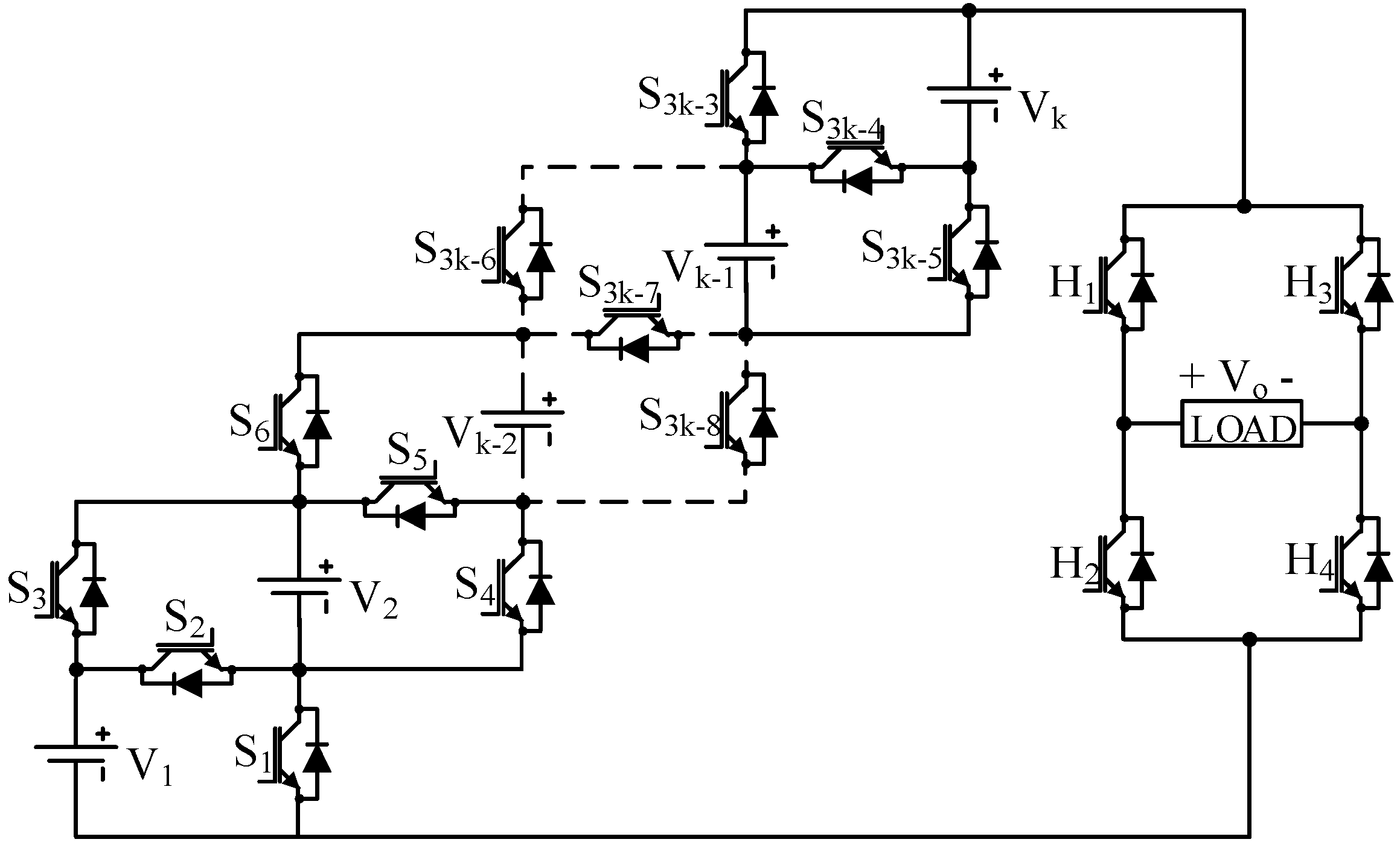
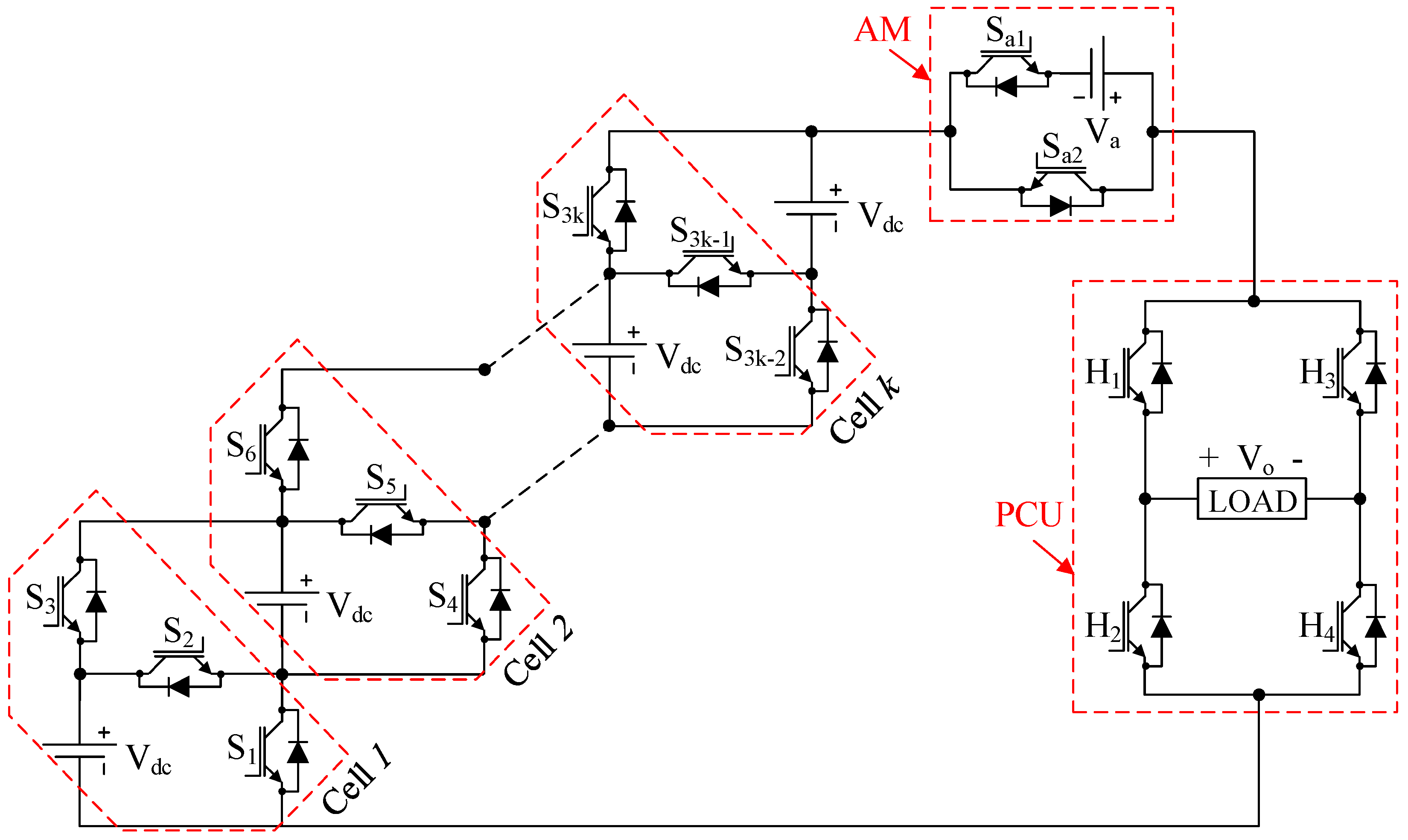
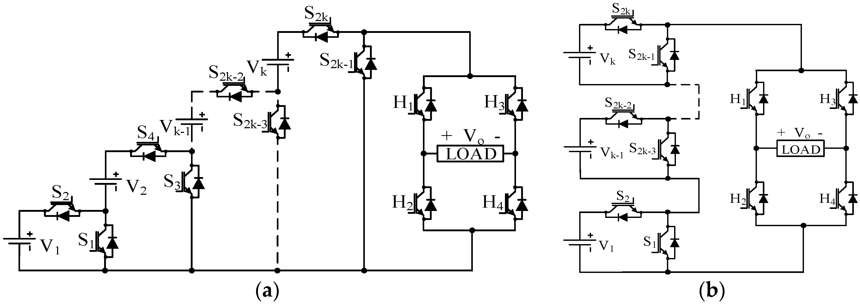
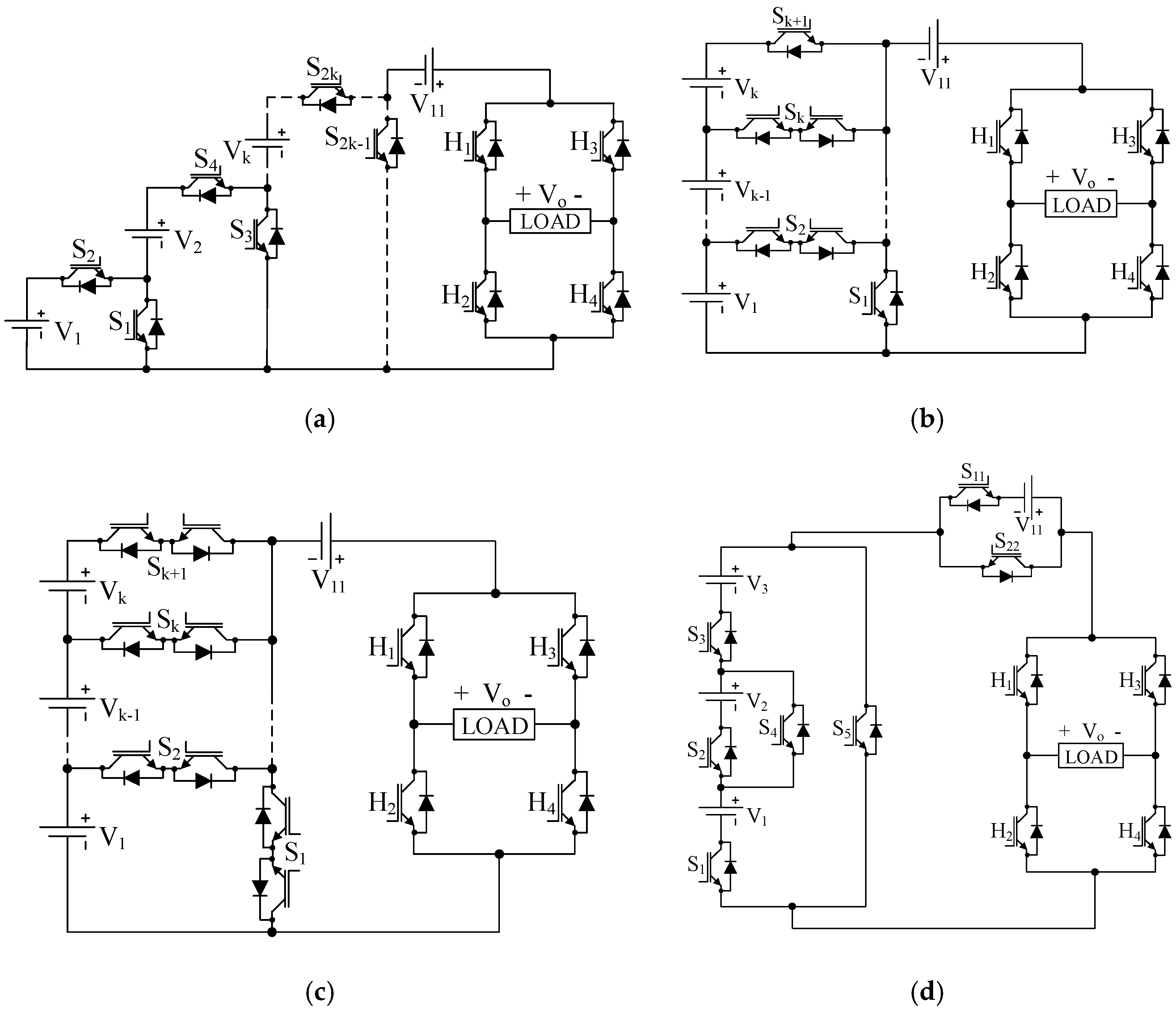
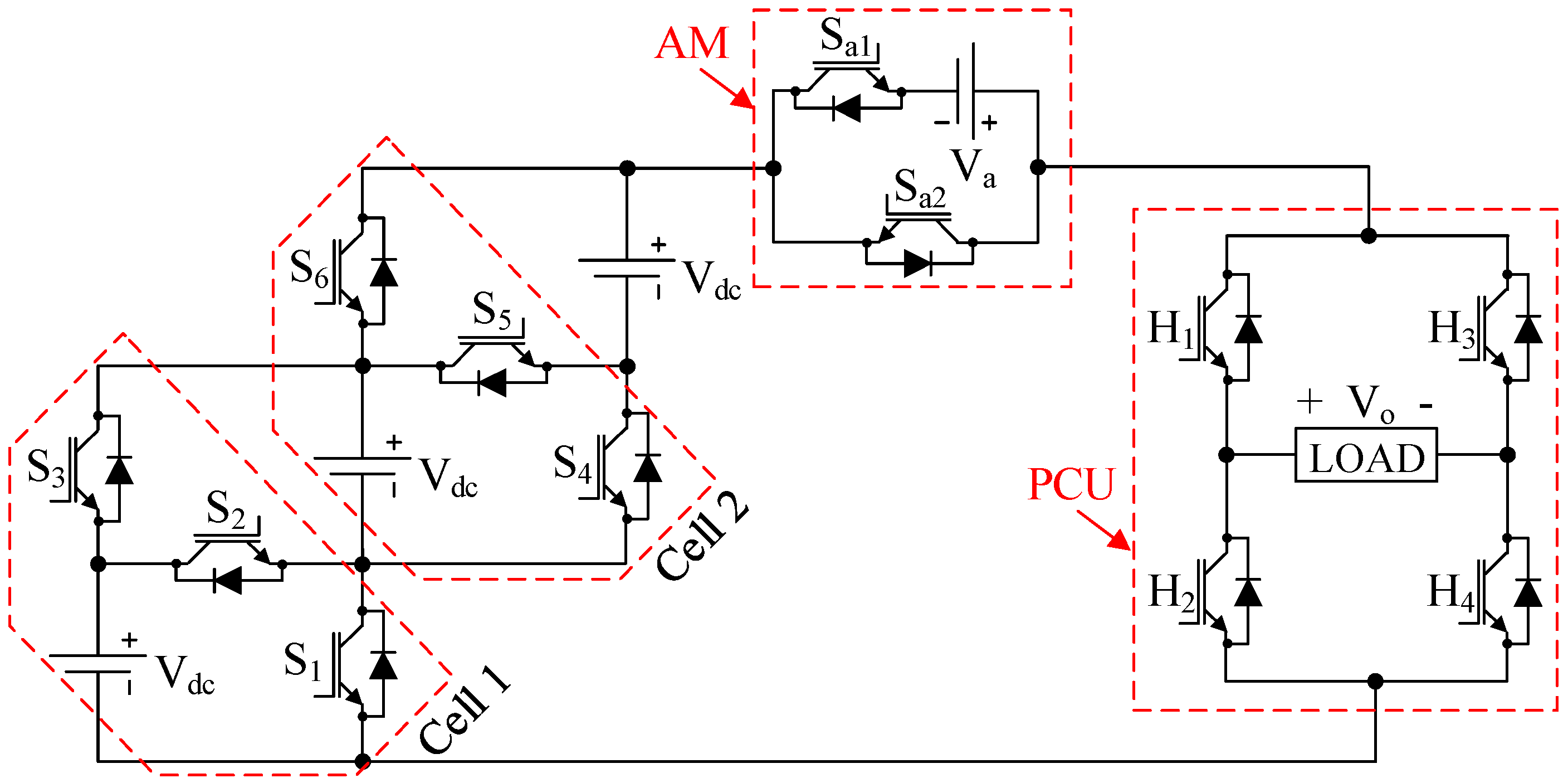
2.1. Generalized Structure of the Topology

The proposed hybrid multilevel inverter topology is shown in Figure 4. It consists of three parts i.e., the level generation module (LGM), the auxiliary module (AM) and the polarity changer unit (PCU).

2.1.1. The Level Generation Module (LGM)

The LGM is built based on the interconnection of k number of cells (k is an integer). Each cell comprises three unidirectional switches and one dc voltage source. The main function of the LGM is to generate all the additive combinations of different dc sources of same magnitude; therefore, the staircase waveform is generated at its output. This is done by utilizing the switches such that the voltage sources of two cells can be connected in series or parallel. For example, if switches S1 and S3 are turned ON, the two dc voltage sources will be connected in parallel in Vdc at the output of LGM. Thus, both cells share the load equally. If switch S2 is turned ON, two dc voltage sources will be connected in series with additive polarity and 2Vdc appears at the output of LGM.
Similarly, several dc voltage sources can be operated in series and parallel combinations to share the load with different voltage levels. The pair of switches (S1, S2) and (S2, S3) should be operated in complementary to avoid the short-circuiting of voltage source V1. A similar operation is required for the kth cell. Moreover, all switches in the LGM operate at low frequency. However, it has to be noted that the LGM cannot produce a zero level at the output because the parallel/series combination of the dc sources will always result in a certain voltage at the output (unless the sources are set to zero, which does not make any sense). Since there is no instant when the output is not connected to the source, the zero level cannot exist at the output at any time.

2.1.2. The Auxiliary Module (AM)

To generate higher number of levels at the output, an auxiliary module (AM) is connected after the LGM. This module comprises one dc voltage source Va and two unidirectional switches Sa1 and Sa2. Both switches need to be operated in a complementary mode to avoid short-circuiting of voltage source Va. When Sa2 is turned ON, the same voltage level generated by the LGM is connected at the output. When Sa1 is turned ON, the voltage source Va is added to the level generated by the LGM. If the magnitude of Va is selected to be half of the dc sources, an intermediate level is formed halfway in between two levels. On the other hand, if Va equals the dc sources, no additional level is formed. Other values of Va result in an unequal intermediate step, which is not desirable. The AM is also used to construct the PWM waveform. Switches Sa1 and Sa2 are modulated similar to the conventional (two-level) inverter.

2.1.3. Polarity Changing Unit (PCU)

The combination of the LGM and AM generates the voltage levels in positive polarity only. To achieve both positive and negative voltage levels at the output, a standard H-bridge is used as a polarity changing unit. Another function of the PCU is to generate the zero voltage level at the output. This is achieved by simultaneously holding the H2 and H4 ON for a certain amount of time.

2.2. Working Principles

The operating principle of the proposed MLI is explained with two cells (k = 2) in the LGM. For the two cells, the topology uses 12 switches and four dc sources, as shown in Figure 5. In order to achieve parallel operation of different dc voltage sources connected to the LGM, the magnitudes of V1, V2, and V3 must be equal. Furthermore, the pair of switches of each cell should operate in a complementary mode to avoid short-circuiting of the dc sources. The switch pairs of the cell include (S1, S2) and (S2, S3). The switching sequences of the parallel operation and complementary pairs are given in Table 1.

2.3. Selection of dc Source Magnitudes

The number of levels at the output is decided by the magnitude of dc voltage sources connected in LGM and AM. For the parallel operation of the proposed MLI, the magnitude of dc sources connected in LGM must be the same. If the magnitude is not equal, the anti-parallel diode connected to an IGBT will conduct, which leads to the short-circuiting of different voltage sources. The MLI can operate in two modes. The magnitude of voltage sources of the AM, i.e., Va determines these modes.

2.3.1. Mode I

Mode I can be considered symmetrical configuration. In this mode, the magnitude of each dc source, including the dc source in the AM, is selected as Vdc. Therefore,
V a = V dc
The number of levels (N) at the output is given as
N = 2 ( k + 1 )

2.3.2. Mode II

A higher number of levels can be realized at the output by changing the magnitude of Va (inside the AM) to Vdc/2. The dc sources connected in LGM remain as before, i.e., each voltage source has a magnitude of Vdc. Using these dc voltages, the number of levels increases to
N = 4 ( k + 1 )
If the zero level generator is activated, N increases by one more step, i.e.,
N = 4 ( k + 1 ) + 1
The number of switches used in the proposed topology is given by
N IGBT = 3 ( k + 2 )
Since all switches are unidirectional, the same number of the driver circuit is required.

2.4. Total Standing Voltage Calculation

The voltage stresses across the switches play an important role in the selection of the power devices. Total standing voltage (TSV) is defined as the sum of maximum voltage stress across all power semiconductor devices considering all voltage levels. The TSV of the proposed topology can be written as
TSV = TSV LGM + TSV AM + TSV PCU
where TSVLGM, TSVAM and TSVPCU represent the TSV of the LGM, AM, and PCU, respectively. The maximum voltage stress across each switch connected in LGM is equal to the magnitude of voltage sources. Therefore
TSV LGM = 3 × k × V dc for   Mode   I   and   II
The voltage stresses across Sa1 and Sa2 are fixed by the magnitude of voltage source Va. Therefore,
TSV AM = 2 × V dc for   Mode   I
and
TSV AM = 2 × 0.5 V dc for   Mode   II
The maximum voltage stress across switches connected in PCU is the sum of all the dc voltage sources connected in the topology. Hence, the TSV of PCU is given by
TSV PCU = 4 ( k + 2 ) × V dc for   Mode   I
and
TSV PCU = 4 ( k + 1.5 ) × V dc for   Mode   II
The TSV of the overall proposed topology is calculated by adding the TSV of all there parts for both modes of operation. From (7)–(11),
TSV = ( 7 k + 10 ) × V dc   for   Mode   I
and
TSV = 7 ( k + 1 ) × V dc for   Mode   II
Hence, for mode I,
TSV = 7 2 ( N + 3 ) × V dc
and, for Mode II,
TSV = 7 4 N × V dc

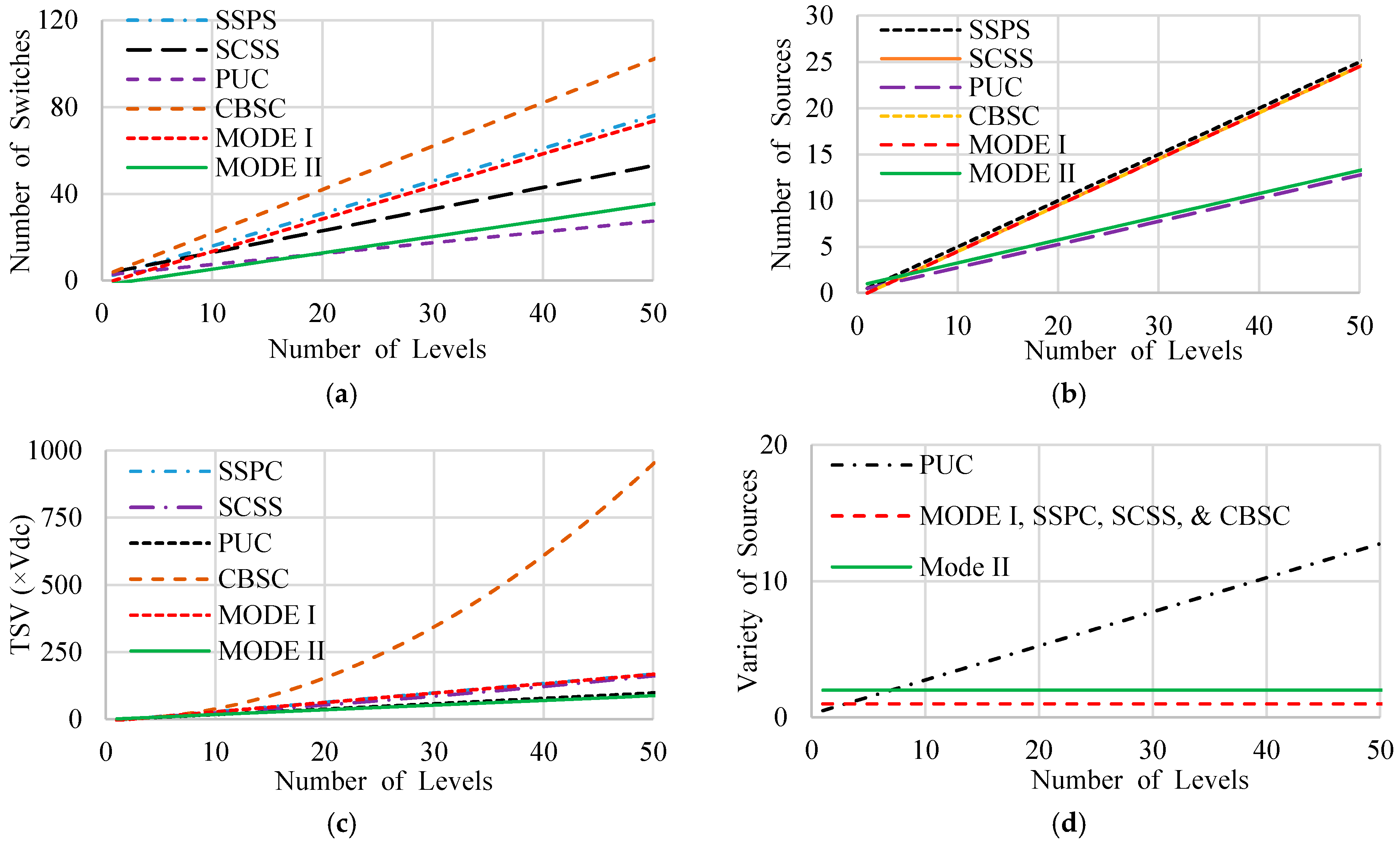
3. Comparative Study

A comparison is made regarding the number of switches, number of dc voltage sources, TSV and variety of dc voltage sources in terms of number of levels. Four similar topologies, i.e., the SSPC, SCSS, PUC, and CBSC MLI, are considered. Figure 6a shows the comparison of the number of switches with respect to the number of levels at the output. From this figure, it is clear that the proposed topology in Mode II requires the least number of switches (for up to 20 levels) compared to other topologies. Furthermore, the proposed topology in Mode I requires fewer switches than CBSC and SSPS topologies. Figure 6b compares the number of dc voltage sources against the number of levels. The proposed topology in Mode II requires a lower number of dc voltage sources, except for PUC. Figure 6c displays the comparison of TSV with respect to the number of levels. When operated in Mode II, the proposed topology has lower TSV than PUC, CBSC and SCSS MLI. In addition, Figure 6d shows the variation of dc voltage sources requires for number of levels at the output. The proposed topology in Mode I requires one variety of the dc voltage source (i.e., one value for all dc sources). In Mode II, it requires two varieties because the Va2 is set to half of Vdc. This is much lower than the variety of dc voltage sources required for the PUC MLI. Overall, the reduced number of switches and dc voltage sources along with lower TSV are the main advantages of the proposed topology.

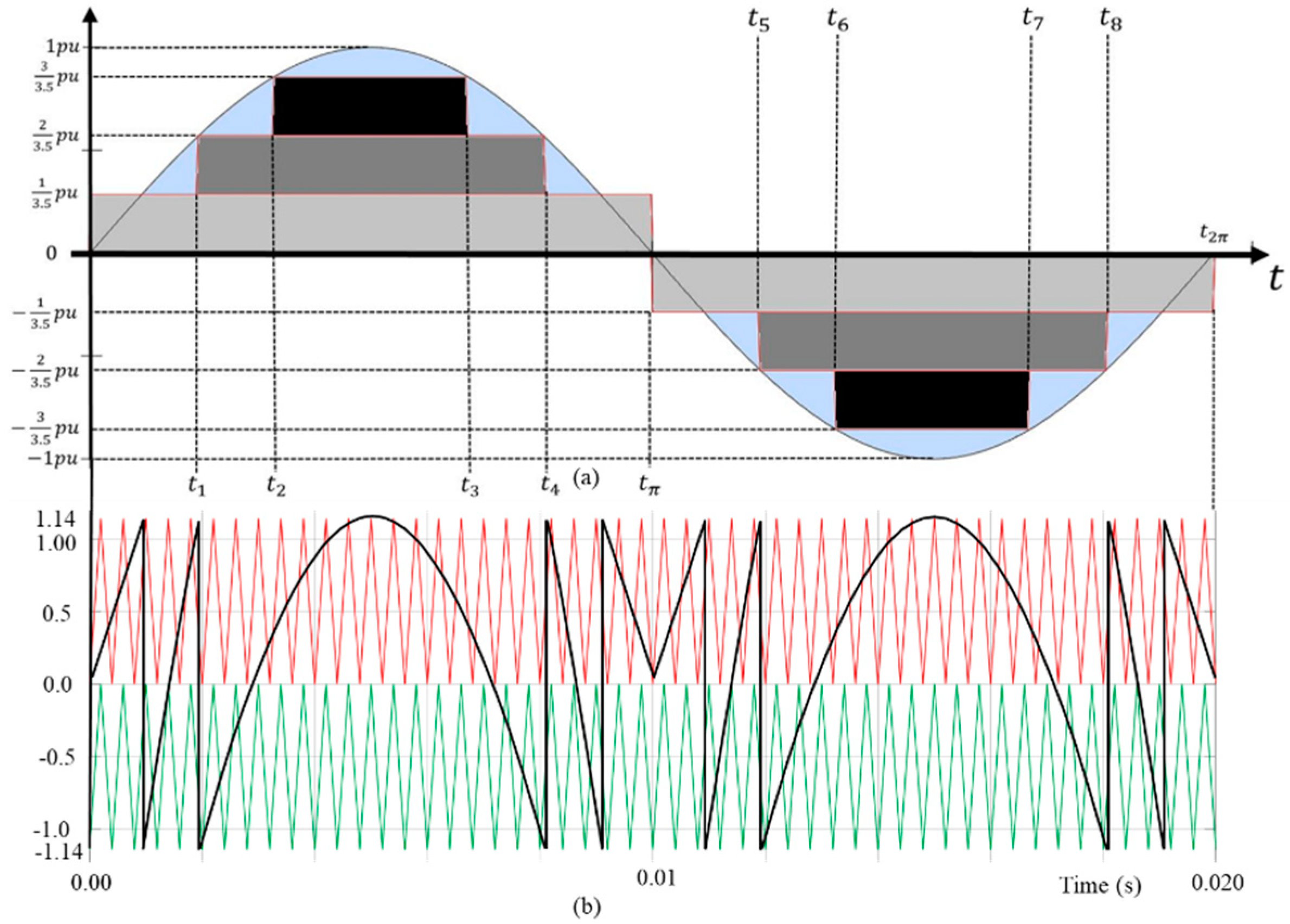
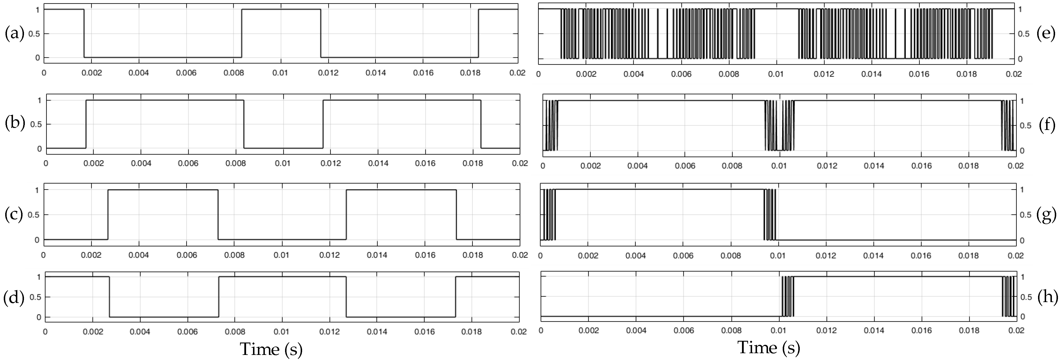
4. Modulation Technique

In this paper, the hybrid modulation technique is utilized [8,26]. To illustrate the technique, a six-level MLI is used. The modulation is divided into two parts. First, the large pulses to drive the LGM switches. This is shown in Figure 7a. It comprises three square waves, each having a peak magnitude of (1/3.5) pu. The negative portion has a magnitude (−1/3.5) pu. These square waves are used to establish the essential part of the sinusoidal reference signal in the positive and negative half cycles. For the positive half cycle, the lower square wave is placed between 0 and tπ. In the negative half cycle, the similar square wave is located between tπ and t. In Figure 7a, the AM circuit is meant to modulate the area in blue. Therefore, the control circuit subtracts the sinusoidal reference wave from the black and grey blocks. The result of this subtraction can be shown in Figure 7b as a blue curve that ranges from −1.14 to 1.14. This curve is modulated with two carriers, the green and the red one. The comparison of the lower square wave and sinusoidal reference signal gives the gate pulses for switches S1 and S2 of the LGM. In the same way, the comparison of other square waves generates the gate pulses for other LGM switches.
For the generation of gate pulses of AM, a differentiated reference signal is created and is shown in Figure 7b. The differentiated reference single is created by locating the area which is not common between sinusoidal reference single and square waves. Each such portion of the sinusoidal signal is placed between (1/3.5) pu and (−1/3.5) pu. This differentiated reference signal is then compared with a carrier signal to generate gate pulses for switches of AM. The overall gate signals generated from this modulation scheme are summarized in Figure 8. These signal labels are consistent with the circuit shown in Figure 5.

5. Results and Discussion

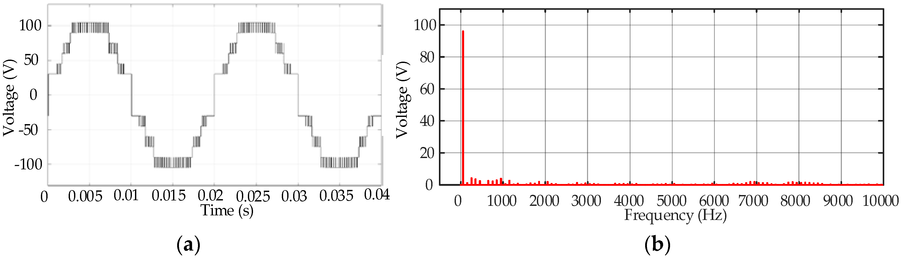
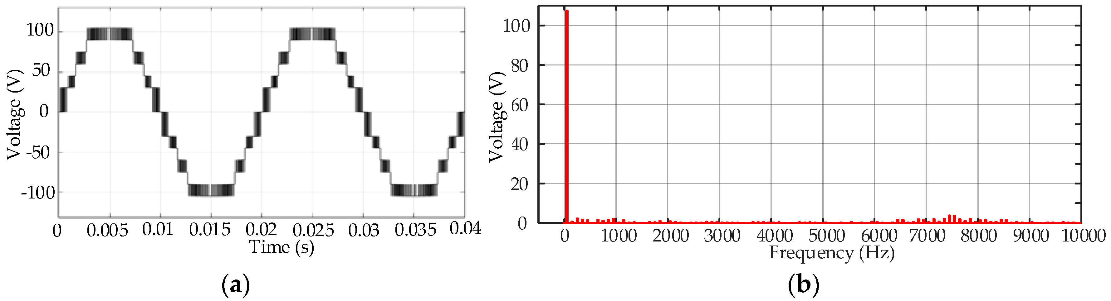
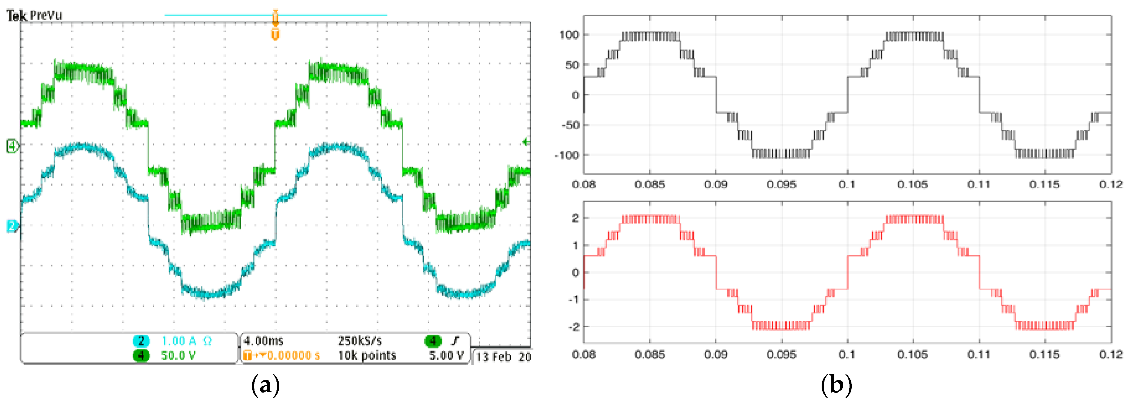
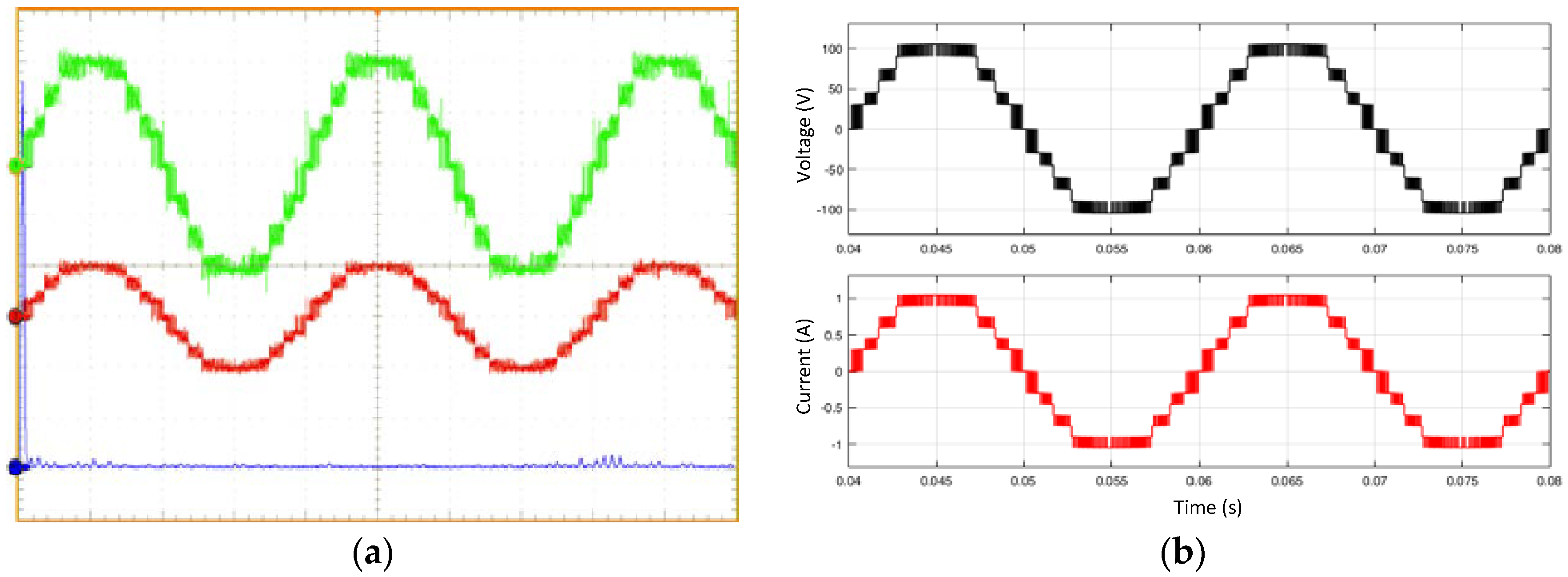
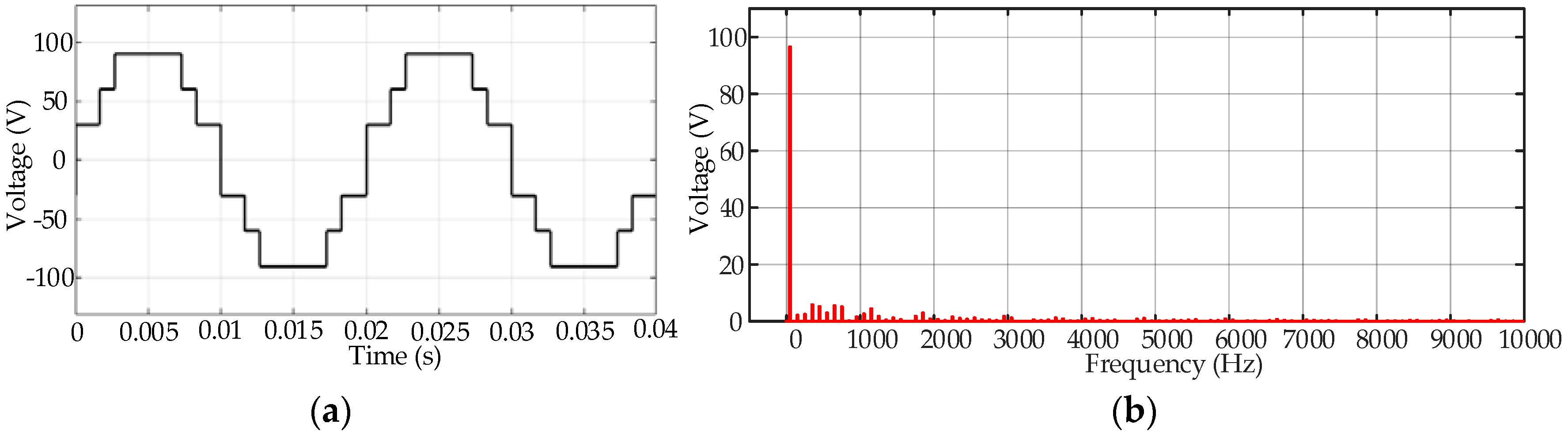
5.1. Simulation Results

The performance of proposed MLI and its modulation strategy is simulated using Matlab/Simulink. Two cells are used (i.e., k = 2) for the simulation results. Therefore, three dc voltage sources are connected to LGM having a magnitude of 30 V. Both modes (Modes I and II) are simulated at a modulation index of 1.14. For Mode I, Va = Vdc = 30 V, while for Mode II, it is half of Vdc, i.e., 15 V. The simulation is performed with a carrier frequency of 7.5 kHz. The square wave pulses for the LGM and PWM for the AM are generated using the modulation technique described in Section 4. For convenience, the simulation is done under a no-load condition because of the emphasis on the correctness of the generated waveforms. The performance with load (R and RL) will be dealt in the experimental section.
The output voltage of the MLI in Mode I is shown in Figure 9a. As expected, the output voltage waveform is of the staircase type as the switches of LGM operate at the fundamental frequency. As can be observed from Figure 9a, the number of levels is 6, which is consistent with Equation (2). Since the dc source is 30 V, the generated levels are 30, 60 and 90 V. Furthermore, the output voltage does not have a zero level, which is inherent to the topology when operated in Mode I. Figure 9b shows the harmonics spectrum without filtering. The computed THD is 15.5%.
When the AM is enabled, i.e., Mode II, additional levels are created. This is shown in Figure 10a. According to Equation (3), the number of levels is increased to twelve. Since Va = 0.5 Vdc, the new levels are located at 45, 75 and 105 V. Furthermore, since the zero level generators are not activated, this level is absent from the waveform. Mode II with the zero level is shown in Figure 11a. Figure 10b and Figure 11b show the harmonic spectrum with and without the zero voltage level generation, respectively. The THD of the former is 12.5%. With the introduction of the zero level, the THD is reduced to 9.5%. Note that these are THD values are without filtering.

5.2. Experimental Verification

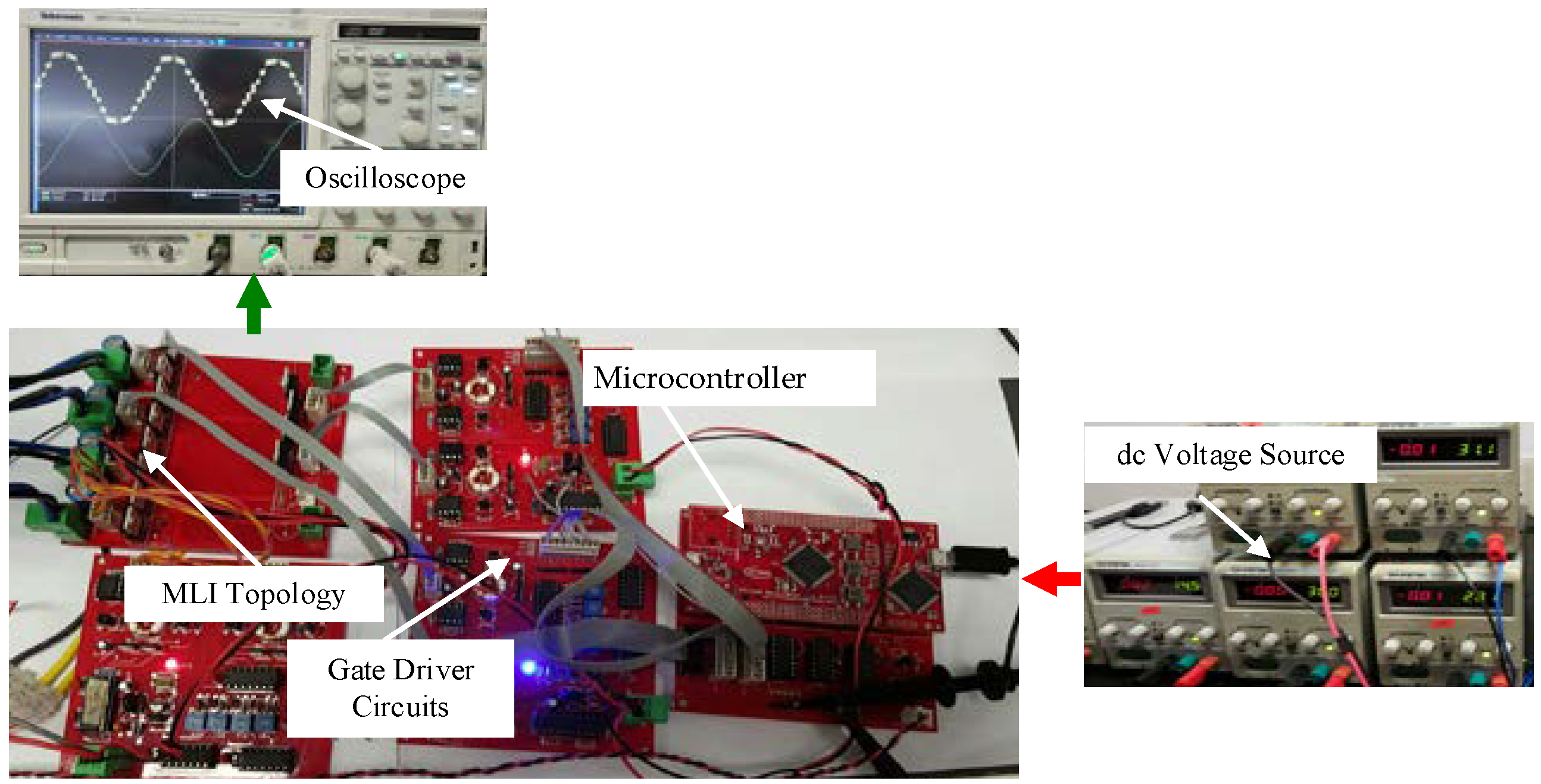
5.2.1. Experimental Setup

To prove the workability of the proposed idea, a 300 W, thirteen level MLI is designed and constructed. Three dc sources are used in LGM (i.e., k = 2); the voltage of each dc source is set to 30 V with one dc voltage source for AM (total of four dc voltage sources are used). The power circuit is based on the IKB20N60H3 IGBT (600 V/20 A). The switching frequency of the PWM waveform for the auxiliary circuit is 7.5 kHz. To implement the modulation, the XE 166 Infineon microcontroller is used. The gate pulses from the microcontroller are made suitable for the switches using the gate driver circuits. A dead time of 0.5 μs is added to protect the bridge from shoot-through fault. The photograph of the MLI arrangement with the dc sources and measurement instrument is shown in Figure 12. Since the inverter is bidirectional, it is tested using the resistive and inductive loads. Furthermore, the auxiliary module can be turned off at convenience; thus, comparison can be readily made for the circuit with and without the auxiliary.

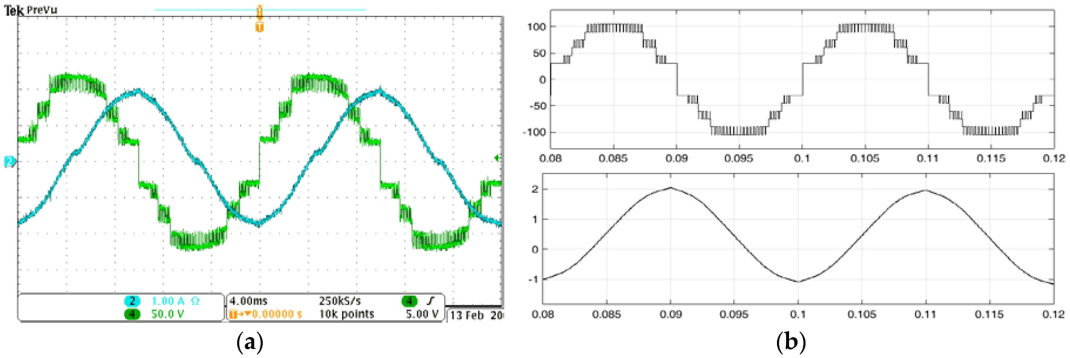
5.2.2. Experimental Results

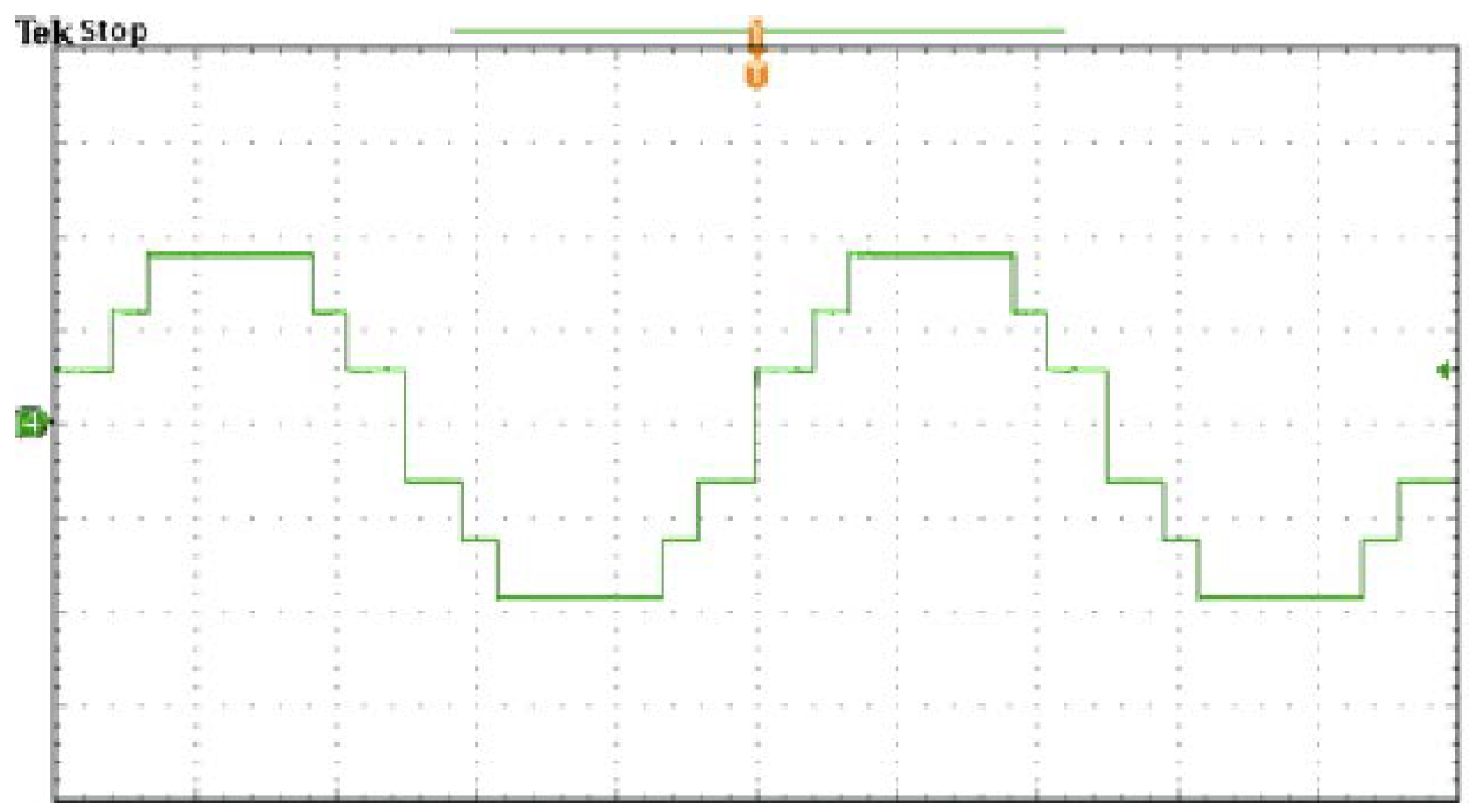
No Load Condition: Mode I and II

Figure 13 shows the experimental output voltage of the MLI in Mode I, under the no-load condition. The modulation index is set to be the same as simulation, i.e., 1.14. As can be observed, the waveform is very similar to the simulation shown in Figure 9a. This confirms the workability of the LGM and the PCU. The output voltage with the AM in Mode II is depicted in Figure 13. The first waveform, i.e., Figure 14a is without the zero level. As expected, the number of levels is increased from six to twelve. The second waveform, i.e., Figure 14b is obtained when the zero level is generated. Again, the experimental waveform is in very close agreement with the simulation, shown by Figure 10a and Figure 11a, respectively.

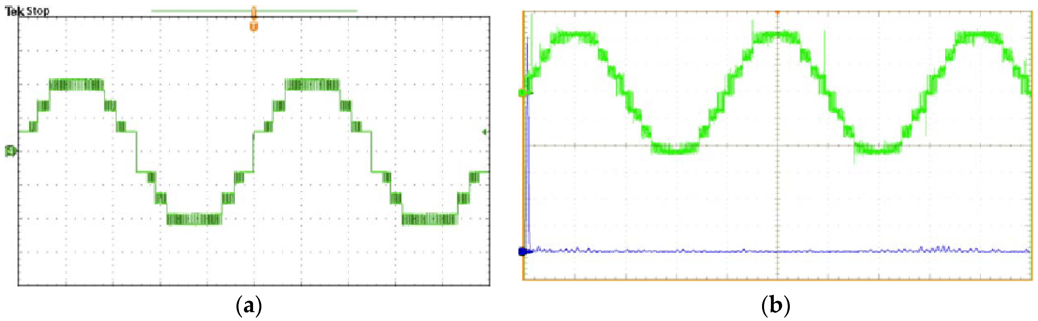
Mode II with Resistive Load

Figure 15a,b show the experimental and simulated output when the MLI is connected to a resistive load (50 Ω) in Mode II. In this case, the zero level is not activated. As expected, for the experimental case, the current follows the voltage, i.e., in phase. However, the waveshape of the former deviates slightly, where the PWM pulses are being rounded at their edges. This is due to the inductive effect of wire wound resistor used as the load. Note that the rounded edges are not observed in the simulation as an ideal resistive load is used in the model.
Figure 16a,b depict the MLI output when the zero level generator is activated. Clearly, the voltage waveform improves due to the introduction of an additional level at the zero crossing point. For all cases, it can be observed that the experimental results are in close agreement with the simulation.

Mode II with Resistive-Inductive Load

Figure 17a demonstrates the experimental waveforms of the MLI in Mode II when connected to an inductive load (R = 10 Ω, L = 250 mH). Figure 17b shows its corresponding simulation waveforms. As can be seen, the current lags the voltage by 83 degrees, which is consistent with the values used in the experiment. Furthermore, it is interesting to note that, a small current distortion occurs at the zero crossing point. The most likely reason for the distortion is the dead-time effect, as suggested by [27]. This fact can be confirmed with the simulated current waveform shown in Figure 17b. As can be seen, the distortion is not present; this is because the dead time is not included in the simulation. Figure 17a,b demonstrate the waveforms of the output voltage and the current, respectively, when the zero crossing generator is connected. There is a slight improvement in the experimental current waveshape. By taking the FFT of the experimental current waveform, the THD without the auxiliary module is 7.6%. For the case with the auxiliary, the THD is reduced to 6.2%. For the simulated current waveforms, the THD is 3.1% and 2.5%, respectively. These results prove that the dead time contributes to more than half of the THD values.

6. Conclusions

In this paper, a new MLI topology with a reduced number of switches and dc voltage sources is recommended. The proposed topology provides enough flexibility for higher voltage and power requirement with series and parallel operation of different dc voltage sources. The notable importance is the sharing of load current among different dc voltage sources. A hybrid modulation technique is used to operate different switches. This modulation scheme provides the high-voltage low-frequency and low-voltage high-frequency operation which reduces the switching losses. The proposed topology is compared with several other similar topologies which indicate the reduction of the number of switches and dc voltage sources. Finally, the performance of the proposed topology is examined by generating 13 levels at the output using MATLAB/Simulink and is verified through experimental results.

Author Contributions

Theoretical observation, simulation, experimental tests, and preparing of the article were done by H.M.B.; Z.S. performed experimental tests and prepared the article.

Funding

The authors would like to acknowledge the financial support received from the Deanship of Scientific Research (DSR) King Abdulaziz University, Jeddah, under grant No (D-086-829-1437).

Conflicts of Interest

The authors proclaim no conflict of interest.

References

  1. Vijeh, M.; Rezanejad, M.; Samadaei, E.; Bertilsson, K. A General Review of Multilevel Inverters Based on Main Submodules: Structural Point of View. IEEE Trans. Power Electron. 2019. [Google Scholar] [CrossRef]
  2. Aganah, K.; Luciano, C.; Ndoye, M.; Murphy, G.; Aganah, K.A.; Luciano, C.; Ndoye, M.; Murphy, G. New Switched-Dual-Source Multilevel Inverter for Symmetrical and Asymmetrical Operation. Energies 2018, 11, 984. [Google Scholar] [CrossRef]
  3. Rodriguez, J.; Lai, J.-S.; Peng, F.Z. Multilevel inverters: A survey of topologies, controls, and applications. IEEE Trans. Ind. Electron. 2002, 49, 724–738. [Google Scholar] [CrossRef]
  4. Kouro, S.; Malinowski, M.; Gopakumar, K.; Pou, J.; Franquelo, L.G.; Wu, B.W.; Rodriguez, J.; Pérez, M.A.; Leon, J.I. Recent Advances and Industrial Applications of Multilevel Converters. IEEE Trans. Ind. Electron. 2010, 57, 2553–2580. [Google Scholar] [CrossRef]
  5. Akagi, H. Multilevel Converters: Fundamental Circuits and Systems. Proc. IEEE 2017, 105, 2048–2065. [Google Scholar] [CrossRef]
  6. Gupta, K.K.; Ranjan, A.; Bhatnagar, P.; Sahu, L.K.; Jain, S. Multilevel Inverter Topologies With Reduced Device Count: A Review. IEEE Trans. Power Electron. 2016, 31, 135–151. [Google Scholar] [CrossRef]
  7. Zhang, J.; Xu, S.; Din, Z.; Hu, X.; Zhang, J.; Xu, S.; Din, Z.; Hu, X. Hybrid Multilevel Converters: Topologies, Evolutions and Verifications. Energies 2019, 12, 615. [Google Scholar] [CrossRef]
  8. Hinago, Y.; Koizumi, H. A Single-Phase Multilevel Inverter Using Switched Series/Parallel DC Voltage Sources. IEEE Trans. Ind. Electron. 2010, 57, 2643–2650. [Google Scholar] [CrossRef]
  9. Lee, F.S.; Kang, S.H. A new structure of H-bridge multilevel inverter. In Proceedings of the KIPE Conference, Jeonnam, Korea, 30 June–3 July 2008; pp. 388–390. [Google Scholar]
  10. Su, G.-J. Multilevel DC-Link Inverter. IEEE Trans. Ind. Appl. 2005, 41, 848–854. [Google Scholar] [CrossRef]
  11. Choi, W.-K.; Kang, F. H-bridge based multilevel inverter using PWM switching function. In Proceedings of the INTELEC 2009—31st International Telecommunications Energy Conference, Incheon, Korea, 18–22 October 2009; pp. 1–5. [Google Scholar]
  12. Samsami, H.; Taheri, A.; Samanbakhsh, R. New bidirectional multilevel inverter topology with staircase cascading for symmetric and asymmetric structures. IET Power Electron. 2017, 10, 1315–1323. [Google Scholar] [CrossRef]
  13. Ebrahimi, J.; Babaei, E.; Gharehpetian, G.B. A New Multilevel Converter Topology With Reduced Number of Power Electronic Components. IEEE Trans. Ind. Electron. 2012, 59, 655–667. [Google Scholar] [CrossRef]
  14. Babaei, E.; Laali, S.; Bayat, Z. A Single-Phase Cascaded Multilevel Inverter Based on a New Basic Unit With Reduced Number of Power Switches. IEEE Trans. Ind. Electron. 2015, 62, 922–929. [Google Scholar] [CrossRef]
  15. Ounejjar, Y.; Al-Haddad, K. A new high power efficiency cascaded U cells multilevel converter. In Proceedings of the 2009 IEEE International Symposium on Industrial Electronics, Seoul, Korea, 5–8 July 2009; pp. 483–488. [Google Scholar]
  16. Ounejjar, Y.; Al-Haddad, K. A novel high energetic efficiency multilevel topology with reduced impact on supply network. In Proceedings of the 2008 34th Annual Conference of IEEE Industrial Electronics, Orlando, FL, USA, 10–13 November 2008; pp. 489–494. [Google Scholar]
  17. Babaei, E. A Cascade Multilevel Converter Topology With Reduced Number of Switches. IEEE Trans. Power Electron. 2008, 23, 2657–2664. [Google Scholar] [CrossRef]
  18. Samadaei, E.; Gholamian, S.A.; Sheikholeslami, A.; Adabi, J. An Envelope Type (E-Type) Module: Asymmetric Multilevel Inverters With Reduced Components. IEEE Trans. Ind. Electron. 2016, 63, 7148–7156. [Google Scholar] [CrossRef]
  19. Samadaei, E.; Sheikholeslami, A.; Gholamian, S.A.; Adabi, J. A Square T-Type (ST-Type) Module for Asymmetrical Multilevel Inverters. IEEE Trans. Power Electron. 2018, 33, 987–996. [Google Scholar] [CrossRef]
  20. Siddique, M.D.; Mekhilef, S.; Shah, N.M.; Memon, M.A. Optimal Design of a New Cascaded Multilevel Inverter Topology with Reduced Switch Count. IEEE Access 2019, 7, 24498–24510. [Google Scholar] [CrossRef]
  21. Alishah, R.S.; Hosseini, S.H.; Babaei, E.; Sabahi, M. A New General Multilevel Converter Topology Based on Cascaded Connection of Submultilevel Units with Reduced Switching Components, DC Sources, and Blocked Voltage by Switches. IEEE Trans. Ind. Electron. 2016, 63, 7157–7164. [Google Scholar] [CrossRef]
  22. Alishah, R.S.; Hosseini, S.H.; Babaei, E.; Sabahi, M. Optimal Design of New Cascaded Switch-Ladder Multilevel Inverter Structure. IEEE Trans. Ind. Electron. 2017, 64, 2072–2080. [Google Scholar] [CrossRef]
  23. Shalchi Alishah, R.; Sabahi, M.; Nazarpour, D.; Hosseini, S.H. Novel multilevel inverter topologies for medium and high-voltage applications with lower values of blocked voltage by switches. IET Power Electron. 2014, 7, 3062–3071. [Google Scholar] [CrossRef]
  24. Shueai Alnamer, S.; Mekhilef, S.; Bin Mokhlis, H.; Shueai Alnamer, S.; Mekhilef, S.; Bin Mokhlis, H. A Four-Level T-Type Neutral Point Piloted Inverter for Solar Energy Applications. Energies 2018, 11, 1546. [Google Scholar] [CrossRef]
  25. Prabaharan, N.; Arun, V.; Sanjeevikumar, P.; Mihet-Popa, L.; Blaabjerg, F.; Prabaharan, N.; Arun, V.; Sanjeevikumar, P.; Mihet-Popa, L.; Blaabjerg, F. Reconfiguration of a Multilevel Inverter with Trapezoidal Pulse Width Modulation. Energies 2018, 11, 2148. [Google Scholar] [CrossRef]
  26. Bassi, H.M. Floating source multilevel inverter uses hybrid double switching frequencies. In Proceedings of the 2017 52nd International Universities Power Engineering Conference (UPEC), Heraklion, Greece, 28–31 August 2017; pp. 1–5. [Google Scholar]
  27. Murai, Y.; Watanabe, T.; Iwasaki, H. Waveform Distortion and Correction Circuit for PWM Inverters with Switching Lag-Times. IEEE Trans. Ind. Appl. 1987, IA-23, 881–886. [Google Scholar] [CrossRef]
Figure 1. The hybrid MLI proposed in [8].
Energies 12 00977 g001
Figure 2. The MLI topologies proposed in (a) [9] and (b) [10].
Energies 12 00977 g002
Figure 3. The hybrid MLI topologies proposed in (a) [11]; (b) [12]; (c) [13]; and (d) [14].
Energies 12 00977 g003
Figure 4. The generalized structure of the proposed multilevel inverter topology.
Energies 12 00977 g004
Figure 5. The proposed MLI topology with two cells.
Energies 12 00977 g005
Figure 6. Comparing the proposed MLI with others in literature (a) number of switches; (b) number of dc sources; (c) total standing voltage (TSV) and (d) variety of dc voltage sources with respect to number of levels.
Energies 12 00977 g006
Figure 7. (a) The hybrid modulation technique and (b) differentiated gate signals with carrier signals.
Energies 12 00977 g007
Figure 8. (a) gate pulses for S1 (LGM); (b) gate pulses for S2 (LGM); (c) gate pulses for S4, (LGM); (d) gate pulses for S5 (LGM); (e) gate pulses for Sa1 (AM); (f) gate pulses for Sa2 (AM); (g) gate pulses for H1 (PCU); and (h) gate pulses for H3 (PCU).
Energies 12 00977 g008
Figure 9. Output of the MLI in Mode I under no-load condition (a) Voltage waveform (b) its corresponding harmonics spectra. THD is 15.5%.
Energies 12 00977 g009
Figure 10. Output of the MLI in Mode II without the introduction of the zero level (a) Voltage waveform (b) its corresponding harmonics spectra. THD is 12.5%.
Energies 12 00977 g010
Figure 11. Output of the MLI in Mode II with the introduction of the zero level (a) Voltage waveform (b) its corresponding harmonics spectra. THD is 9.5%.
Energies 12 00977 g011
Figure 12. The photograph of the prototype MLI circuit.
Energies 12 00977 g012
Figure 13. The experimental output voltage (top trace) in Mode I: no load condition. (Scale: vertical: 50 V/div, horizontal: 4.0 ms/div).
Energies 12 00977 g013
Figure 14. The experimental output voltage in Mode II: no load condition (a) without zero level (b) with zero level Scale for (a): vertical: 50 V/div, horizontal: 4.0 ms/div). Scale for (b): vertical: 50 V/div, horizontal: 5.0 ms/div).
Energies 12 00977 g014
Figure 15. The output voltage (top trace) and current (bottom trace) waveforms with resistive load (50 Ω) without the auxiliary module. (a) experimental (b) simulation result. Experimental scale (50 V/div, 1 A/div, 4.0 ms/div).
Energies 12 00977 g015
Figure 16. The output voltage (top trace) and current (bottom trace) waveforms with resistive load (50 Ω) with the auxiliary module. (a) experimental (b) simulation result. Experimental scale (50 V/div, 1 A/div, 5.00 ms/div).
Energies 12 00977 g016
Figure 17. The output voltage (top trace) and current (bottom trace) waveforms with resistive load (50 Ω) in Mode II without the zero level. (a) experimental (b) simulation result. Experimental (50 V/div, 1 A/div, 4.00 ms/div).
Energies 12 00977 g017
Table 1. Switching table with two cells.
S1/S3S2S4/S6S5Sa1Sa2H1H2H3H4Vo
00000001010
1010011001Vdc
1010101001Vdc + Va
01100110012Vdc
01101010012Vdc + Va
01010110013Vdc
01011010013Vdc + Va
00000010100
1010010110−Vdc
1010100110−(Vdc + Va)
0110010110−2Vdc
0110100110−(2Vdc + Va)
0101010110−3Vdc
0101100110−(3Vdc + Va)

