Abstract
The application of thinner cadmium sulfide (CdS) window layer is a feasible approach to improve the performance of cadmium telluride (CdTe) thin film solar cells. However, the reduction of compactness and continuity of thinner CdS always deteriorates the device performance. In this work, transparent Al2O3 films with different thicknesses, deposited by using atomic layer deposition (ALD), were utilized as buffer layers between the front electrode transparent conductive oxide (TCO) and CdS layers to solve this problem, and then, thin-film solar cells with a structure of TCO/Al2O3/CdS/CdTe/BC/Ni were fabricated. The characteristics of the ALD-Al2O3 films were studied by UV–visible transmittance spectrum, Raman spectroscopy, and atomic force microscopy (AFM). The light and dark J–V performances of solar cells were also measured by specific instrumentations. The transmittance measurement conducted on the TCO/Al2O3 films verified that the transmittance of TCO/Al2O3 were comparable to that of single TCO layer, meaning that no extra absorption loss occurred when Al2O3 buffer layers were introduced into cells. Furthermore, due to the advantages of the ALD method, the ALD-Al2O3 buffer layers formed an extremely continuous and uniform coverage on the substrates to effectively fill and block the tiny leakage channels in CdS/CdTe polycrystalline films and improve the characteristics of the interface between TCO and CdS. However, as the thickness of alumina increased, the negative effects of cells were gradually exposed, especially the increase of the series resistance (Rs) and the more serious “roll-over” phenomenon. Finally, the cell conversion efficiency (η) of more than 13.0% accompanied by optimized uniformity performances was successfully achieved corresponding to the 10 nm thick ALD-Al2O3 thin film.
1. Introduction
In order to improve the short-wave response and increase the short circuit current density (Jsc) of the cadmium sulfide (CdS)/cadmium telluride (CdTe) cell, it is necessary to reduce the photon absorption of the CdS window layer. One useful method is to reduce the thickness of the CdS film [1]. When the thickness of CdS exceeds 100 nm, there is a strong absorption of photons with energy measuring greater than 2.4 eV, meaning that the number of photons reaching the junction region is substantially reduced, which leads to a reduction in photocurrent [2]. However, when the thickness of CdS is reduced to below 50 nm, some fine pinholes begin to emerge because of the reduction of compactness and continuity of the CdS film, resulting in the destruction of the CdS/CdTe heterojunction. In extreme cases, some local short circuit channels are formed by the direct contact of the absorption layer of CdTe with the front electrode transparent conductive oxides (TCO) through larger pinholes. Therefore, in the case of the thinner window layer, a buffer layer having a relatively high resistance between TCO and CdS is necessary to block the direct contact between the CdTe and the front electrode [3,4]. Furthermore, this buffer layer must also have a high transmittance in the full spectrum to avoid the loss of absorbed light. As one of the candidate materials for the buffer layer, alumina has the advantages of abundant resources, low cost, and good thermal and chemical stability. Furthermore, Al2O3 has been currently employed as passivation and anti-diffusion layers in solar cells [5,6,7], especially in the passivated emitter and rear cell, which is attributed to alumina that has a band gap of 8.8 eV greater than that of the TCO substrate but has a stable interface with a low density of states at Al2O3 and TCO and also has a high density of fixed negative charges (~1013 cm−2). As a passivation layer, Al2O3 has been mainly used in p-type materials, because it can significantly reduce the surface electron concentration [8]. It is well known that the resistance of the aluminum oxide film is very large. So, it is especially important to precisely control the thickness of alumina to avoid the effect of the extra series resistance in cells brought by the Al2O3 buffer layer, as well as to ensure the formation of a dense continuous Al2O3 thin film to avoid extra leakage channels in the case of relatively small thickness (<20 nm) of the Al2O3 thin film. Thus, choosing an appropriate fabrication technology is critical for achieving the corresponding blocking function of the Al2O3 buffer layer.
As a special chemical vapor deposition technology with lower temperature, quasi-continuous and self-limiting characteristics atomic layer deposition (ALD) is a preferred method to deposit an ultra-thin-film layer due to its ability to deposit high-quality and uniform materials with an atomic-level precise control of layer thickness. For this technology, gaseous chemical precursors are alternately introduced into the reaction chamber in a pulsed manner to generate a gas–solid chemical reaction on the substrate, thereby forming a dense, uniform, pinhole-free, and continuous film containing fewer impurities on the substrate. This deposition technique is very suitable for those substrates with undulating surfaces and facilitates the formation of a continuous ultra-thin film on the grooves or channels in substrate, thus effectively blocking the potential leakage paths, which cannot be achieved by other deposition techniques [9,10]. Al2O3 films were widely used as a passivation layer in p-silicon solar cells, while its application in cadmium telluride thin film solar cells was relatively rare [11,12]. Kephart et al. studied the application of sputter-deposited oxides for interface passivation in CdTe photovoltaics and found that Al2O3 shows the strongest passivation effect at the front interface and the highest lifetime and Photoluminescence (PL) intensity improvement at the rear interface. It is worth noting that the basic structure of their cells was MZO/CdTe, in which the window layer CdS was totally replaced with MgZnO [13].
Based on the above analysis, in this work, ALD technology was used to fabricate Al2O3 films with different thicknesses on TCO. The optical, electrical, and structural properties of TCO/Al2O3 films were analyzed. Then these films were applied in CdS/CdTe solar cells with a 40-nm-thick CdS, and the performances of the cells were studied at the same time. Finally, the potential application of alumina as a buffer layer in CdS/CdTe thin film solar cells was clarified.
2. Experimental
Atomic layer deposition equipment ALD100-R produced by GuoKai Electronic Co., Ltd. was employed to prepare Al2O3 films. The TCO films commonly used in our laboratory were selected as the substrate, namely TEC 10, which was a commercial glass coated with FTO (SnO2:F).
The experimental conditions of ALD-Al2O3 fabrication were as follows: Substrate temperature was 150 °C, purge time was 30 s, dose time was 0.3 s, and the action time was 15 s. High-purity water supplying element O of Al2O3 and trimethylaluminum (TMA) supplying Al of Al2O3 with a purity of 99.999% were used as precursors, and ultrahigh purity 99.9999% N2 was used as the carrier and purging gas with a constant flow rate of 20 sccm throughout all cycles during ALD deposition. ALD cycling began with H2O exposure to the substrate surface with a hydroxyl group for action with the first TMA pulse. After each precursor exposure, the ALD chamber and gas feeding lines were purged with N2 to prevent chemical vapor deposition from occurring, followed by the next cycle. The test method for the thickness of ALD-Al2O3 is shown in Figure 1, and the schematic of the reaction mechanism of ALD is shown in the inset of Figure 1. The thickness d of the aluminum oxide film was calculated according to the following formula: , where C is the capacitance value of the capacitor device composed of p-Si as one electrode and an ALD-Al2O3 and Ti(3 nm)/Au(40 nm) electrode prepared by electron beam evaporation (EBE) with an area of 0.05 mm2, is 8.85 × 10⁻¹² F/m, and is 9 [14]. In this work, a complete cycle corresponded to a thickness of 0.33 nm for Al2O3 deposition, which was twice greater than other published results of ~0.15 nm/cycle [11,15]. Therefore, the corresponding Al2O3 thickness was obtained by controlling the number of cycles, i.e., 3 cycles corresponded to 1 nm, 15 cycles to 5 nm, 30 cycles to 10 nm, and 60 cycles to 20 nm, respectively. Next, after the CdS thin film with a thickness of 40 nm was deposited by using chemical bath deposition (CBD) technique on the surface of ALD-Al2O3 at about 85 °C, CdTe thin film with a thickness of 5 µm was prepared by using close-space sublimation (CSS) method. The deposition conditions of CdTe were as follows: The chamber was initially evacuated to a pressure of 5 × 10⁻² Pa, and a mixture of 99.999% pure argon and 99.999% oxygen (the oxygen partial pressure was 8%) was then charged into the chamber to maintain a pressure of 1 KPa; the space from the substrate to the source was 2 mm; and the source and substrate were simultaneously heated to about 650 °C and 550 °C, respectively, and the deposition time for CdTe was 5 min. Afterwards, the CdTe films were annealed for 30 min with the CdCl2 source in a tube furnace preheated to 380 °C under 1 atmospheric pressure of mixed N2 + O2 gas (volume ratio 4:1). Before the back-contact deposition, the CdTe film was etched by bromine methanol solution to purify the surface. The concentration of the bromine methanol solution was 0.2%, and the duration was 4 s. Then, a back-contact layer of ZnTe:Cu which was used to reduce the contact resistance between CdTe and the back-electrode metal, was fabricated by using a vacuum thermal evaporation technique. Then, 99.999% pure ZnTe and 99.999% pure Cu powder were put into quartz crucibles and heated indirectly by tungsten heater and molybdenum heater, respectively. Two quartz crystal monitors were employed to monitor the deposition rates of ZnTe and Cu on-line, respectively. Finally, unit cells with areas of 0.24 cm2 were achieved by depositing a 100-nm-thick nickel electrode using EBE with a shadow mask. The structure of the solar cells is shown in Figure 2.
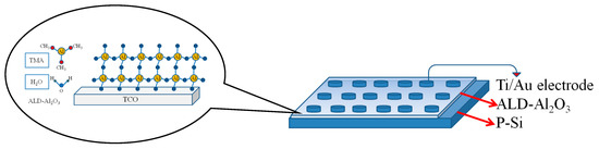
Figure 1.
Schematic diagram of test method for the thickness of atomic layer deposition (ALD)-Al2O3 thin films, the schematic of reaction mechanism of ALD is also shown in the left inset.
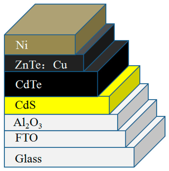
Figure 2.
The structure of a cadmium sulfide (CdS)/cadmium telluride (CdTe) solar cell with ALD-Al2O3.
3. Results and Discussion
3.1. Optical Properties
Figure 3a shows the transmittance spectra of TCO/Al2O3 films utilized by UV/Vis spectrometer (Lambda 9500 PerkinElmer). One may find that the curves of all the samples exhibited a relatively insensitive variation in transmittance with the increase of the thickness of Al2O3, and a high transmittance (>85%) for visible light with a wavelength of >400 nm was easily observed. Additionally, all the curves showed an obvious sharp absorption edge at the wavelengths of around 300 nm, which was anticipated from the band gap Eg of the substrate calculated by Tauc formula as follows:
where α is the absorption coefficient, which is related to the thickness of the film, is defined as photon energy, A is a constant, and the value of n depends on the energy-band structure of the material. For direct energy-band semiconductor materials, such as SnO2, n is 0.5 [16]. The obtained Eg was 4.33 eV for TEC 10, agreeing well with the former result [17]. Notably, no obvious extra absorption of photons was caused, as Al2O3 was introduced onto the substrate because of the fact that the Eg of Al2O3~8.8 eV is far greater than that of the substrate. So, according to the change in Figure 3a, ALD-Al2O3 films with excellent light transmittance are suitable to be served as buffer layers between the front electrode TCO and the window layer CdS.
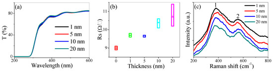
Figure 3.
(a) Transmittance vs. wavelength spectra, (b) sheet resistance, and (c) Raman spectra of the TEC 10/ALD-Al2O3 thin films with different Al2O3 thickness.
3.2. Electrical Properties
Figure 3b shows the sheet resistance of the TEC 10/Al2O3 thin film tested by a four-point probe resistivity measurement system (PROBES TECH). With the increase of the thickness of Al2O3, not only an upward tendency but also the appreciable variations of the sheet resistance of the samples were observed. As compared with the bare substrate, the sheet resistance of the TEC 10 substrate coated by 10 nm Al2O3 increased by 15.22%. Furthermore, the resistance non-uniformity of the TEC 10 substrate with 10 nm thick Al2O3 was 4.83% while that of TEC 10 with 20 nm thick Al2O3 increased to 11.11%, with the magnitude of the increase exceeding 130%. This is caused by the modification of the surface characteristics of the substrate. With the increase of the ALD deposition cycle, Al2O3 accumulated locally in the pores or cavities on the substrate surface leading to the local ALD-Al2O3 thickness exceeding the designed deposition thickness, which resulted in the increase of electrical non-uniformity [18]. Combined with the device performance, the non-uniform sheet resistance had a great influence on the device performance, especially in the fill factor.
3.3. Structural Properties
Raman spectra of ALD-Al2O3 with different thicknesses on the TEC 10 substrate were taken using laser Raman spectrometer (Lab RAM HR HORIBA) with a grating of 600 g/mm, and the exciting lasers of a wavelength of 785 nm were employed with comparable beam spots ~2 μm in diameter. Only two peaks at 370 cm−1 and 560 cm−1 could be observed in Figure 3c. The peak shape was not sharp enough, accompanied by a distinct shoulder peak, and the full width of the half maximum of the peaks was also big, which verified that the ALD-Al2O3 film deposited at 150 °C had an amorphous structure [19]. The first peak at about 370 cm−1 might be attributable to alumina, but it could also be a result of the combination of SnO2:F (this mode B1g often corresponded to 360 cm−1) and amorphous Al2O3, which may be attributable to the fact that the phonon scattering range was closely related to the grain size and the surface stress of the film. The peak at 560 cm−1 was assigned to the characteristic Raman shift peak of the substrate SnO2:F [20,21,22].
3.4. Surface Morphology
Surface morphology characterization for ALD-Al2O3 deposited on TEC 10 was accomplished by employing atomic force microscopy (AFM, Bruker Multi Mode 8), as shown in Figure 4. Meanwhile, the corresponding roughness was also listed in Table 1. Arithmetic mean roughness (Rq) and root-mean-square roughness (Ra) of the substrate without alumina were 17.2 nm and 13.9 nm, respectively, while the Rq and Ra of the substrate with 1 nm alumina increased to 19.0 nm and 15.1 nm, respectively. This change might be due to the substrate temperature 150 °C. However, it could be seen that as the number of Al2O3 deposition cycles increased, the surface roughness of the film gradually decreased. The Rq of 1 nm thick Al2O3 film was 19.0 nm while that of 20 nm thick Al2O3 film was 15.5 nm, with a 18.4% reduction, and the corresponding Ra also decreased by 17.2%, which revealed that the surface smoothness of TCO/ALD-Al2O3 thin films was improved and this variation was attributed to the filler Al2O3 in the pores or cavities on the substrate surface. Furthermore, it could also be seen that the particle size was uniform, and there was no large-particle alumina clusters or obvious wrinkles on the film surface, which indicated that the Al2O3 was uniformly distributed on the surface of the TEC 10 substrate. These change trends were quite conducive to promoting the quality of the subsequent deposition process of CdS films and reducing the interface defect states. However, as shown in Figure 4, because the thickness of the ALD-Al2O3 was not more than 20 nm while the peak-to-valley distances of the substrate exceeded 100 nm, a very smooth surface had not yet been obtained in this work, although the roughness of the surface of the sample had improved to some extent.
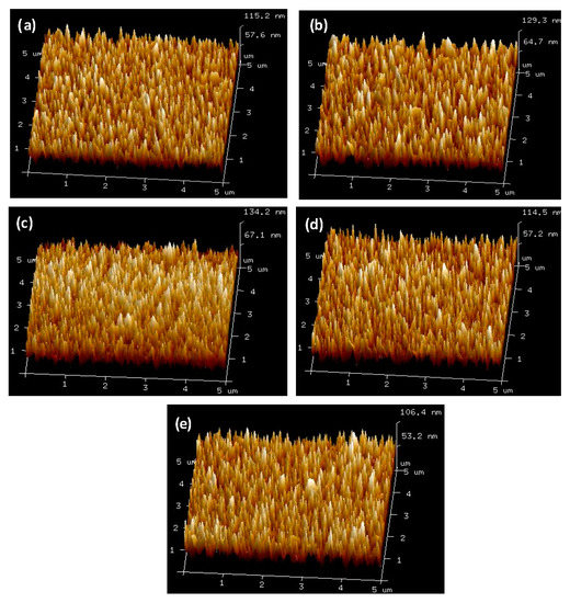
Figure 4.
Atomic force microscopy (AFM) pictures of the TEC 10/ALD-Al2O3 thin films with different Al2O3 thickness, (a–e) corresponding to the thickness of 0 nm, 1 nm, 5 nm, 10 nm, and 20 nm, respectively.

Table 1.
The properties of the TEC 10/ALD-Al2O3 films, arithmetic mean roughness (Rq), root-mean-square roughness (Ra) and the average performances of solar cells, conversion efficiency (η), shunt resistance (Rsh), series resistance (Rs), fill factor (FF), short circuit current density (Jsc), open circuit voltage (Voc), dark reverse saturation current density (J0).
3.5. Devices Performances
Finally, according to the International Electrotechnical Commission (IEC) 61646, the transient photocurrent-voltage was tested by using a specialized solar cell tester under an irradiance of 1000 W/m2 at 25 °C, and the dark current versus voltage curves were also measured at a bias range of −0.8 V to 1.2 V by using an Agilent 4155C semiconductor parameter analyzer. The characterization was carried out on 10 champion cells with different Al2O3 thickness and the results were summarized in Figure 5 while the average parameters were listed in Table 1. As the thickness of the alumina increased from 0 nm to 20 nm, some parameters showed a more fluctuating change. For example, the shunt resistance (Rsh) increased first and then decreased while the series resistance (Rs) maintained a tendency to increase. The Jsc of the cells was relatively insensitive to variations in the change of ALD-Al2O3 thickness due to the fact that the thickness of the window layer CdS was fixed at 40 nm in all cells. Interestingly, the conversion efficiency (η) showed exactly the same open circuit voltage (Voc) and fill factor (FF) behavior with an optimized value corresponding to the 10 nm thick ALD-Al2O3 buffer layers. Furthermore, as can be seen in Figure 5, after the alumina was introduced between TCO and CdS, the uniformity of the cell performance was significantly improved. Taking the conversion efficiency as an example, for the cells without alumina, the efficiency variation (∆η/ηmax) was 21.34%, and those of the cells with an alumina thickness of 1 nm, 5 nm, and 10 nm were 18.23%, 9.85%, and 7.37%, respectively. However, as the thickness of the alumina continually increased, the fluctuation in efficiency began to increase. Finally, a cell with a conversion efficiency of 13.40% was obtained, which was attributed to the fact that the leakage paths (including grain boundaries and pinholes) generated by the very thin CdS can be effectively blocked by introducing the ALD-Al2O3 between TEC 10 and CdS. At the same time, the increase in sheet resistance of TEC 10/10 nm ALD-Al2O3, as shown in Figure 3b, also helped block the leakage channels caused by the pinholes formed in the thinner CdS layer and optimized the CdS/CdTe heterojunction characteristics, which provided evidence of the existence of the alumina blocking effect. Furthermore, the thickness of the ALD-Al2O3 thin film as a buffer layer had multiple effects on the performances of the cells: the average performance degradation of cells with the 20 nm thick ALD-Al2O3 was visible with a 10.0% and 9.3% decrease in Voc and FF, respectively, compared to those of cells with the 10 nm thick ALD-Al2O3. As a result, the η of the cell declined by 20.0%. This degradation was caused not only by the increase in Rs (9.2%), but also by the decrease in Rsh as a function of the transportation properties of thermally excited electrons through the barriers at the interface [23].
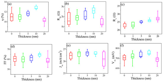
Figure 5.
The performance parameters of CdS/CdTe solar cells with different Al2O3 thicknesses, (a–f) corresponding to conversion efficiency (η), Rsh, Rs, FF, Jsc, and Voc, respectively.
The representative photocurrent and dark current curves of cells with performances close to the average performance of all the cells are shown in Figure 6. The typical cell performance shown in Figure 6a demonstrated the same tendency of change as analyzed above. As shown in Figure 6b, under the reverse bias or a small forward bias, the current was very small and relatively insensitive to variation in bias. However, an exponential increase trend of dark current could be clearly observed when the forward bias exceeded 0.6 V, close to the value of Voc of solar cells. The CdTe heterojunction current is described as follows [24]:
where I0 is the dark reverse saturation current, K is Boltzmann’s constant, A is defined as the diode ideality factor representing the diffusion and recombination current components, and in this work, T is 298 K. The corresponding values of J0 (dark reverse saturation current density) are listed in Table 1, and the values of A in this work were close to 2. With the increase of alumina thickness, the J0 of cells decreased, revealing that the characteristics of the CdS/CdTe heterojunction were improved, and the negative effects of pinholes produced by CdS thin film were effectively suppressed. However, when the thickness of the alumina increased to 20 nm, the J0 increased to 13.0 × 10⁻⁸ mA/cm2, which verifies the attenuation of the junction characteristics. It was worth noted that when the bias voltage exceeded 0.9 V greater than the Voc of the devices, an “inflection point” of the current could be obviously observed; this was the “roll over” phenomenon. Because the work function of CdTe is ~5.7 eV higher than that of the common metals used as the back electrode, the “roll-over” phenomenon will then be induced by the Schottky barrier formed at the CdTe/back electrode interface in the J–V curves was easily observed in the CdS/CdTe solar cells. An effective way to reduce this phenomenon is to introduce a back-contact layer between the CdTe and back electrode to form an ohmic back contact [25,26]. As shown in Figure 6b, in which the “roll over” phenomenon was greatly weakened, the difference was attributed to the fact that the buffer layer ZnTe:Cu was introduced as a back contact in all the solar cells fabricated in this work, and the effect of the metal/CdTe Schottky junction with a direction opposite to that of the main junction CdS/CdTe was effectively reduced. However, the “roll over” phenomenon became more serious when the alumina was introduced in the cells. According to reference [27], this “roll-over” phenomenon can also be introduced by other reasons, such as a relatively large positive conduction band offset at the interface of the CdS and CdTe films. In this work, the cause of this phenomenon might have been that the alumina formed an energy barrier that could not be ignored at the interface of Al2O3/CdS [28].
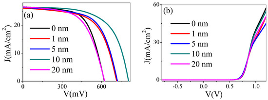
Figure 6.
(a) Typical photocurrent and (b) dark current curves of the CdS/CdTe heterojunction solar cells for each ALD-Al2O3 thin film thickness.
4. Conclusions
In summary, we have successfully prepared alumina thin films by ALD and ALD-Al2O3 buffers have been incorporated into CdS/CdTe based solar cells. The amorphous ALD-Al2O3 is transparent to visible light and smoothens the surface of TCO. The device performance is significantly improved by the utilization of ALD-Al2O3 buffers and an optimized power conversion efficiency of over 13% has been achieved. Therefore, combined with the representative results of cells, the introduction of alumina is a comprehensive consideration process, especially in the control of its thickness. Fortunately, ALD technology meets the requirements for the precise control of alumina thickness. In this work, we confirm the possibility of the ALD-Al2O3 buffer in CdTe solar cells and pave a way to further optimize the device performance of CdTe and other photovoltaic devices which are suffered from surface/interface passivation problems.
Author Contributions
G.Z. and X.H. carried out the experiment, analyzed the results and wrote the manuscript; S.R., carried out the experiment. L.F. and Q.W. gave their modification suggestions for the manuscript.
Funding
This research was funded by National Key Research and Development Program of China: Newton Fund-China-UK Research and Innovations Bridges 2016YFE0124500, School-Enterprise Cooperation Project 17H0242 and Sichuan Provincial Human Resources and Social Security Department Science and Technology Project 201814576.
Conflicts of Interest
The authors declare no conflict of interest.
References
- Zeng, G.G.; Zheng, J.G.; Li, B.; Lei, Z.; Wu, L.L.; Cai, Y.P.; Li, W.; Zhang, J.Q.; Cai, W.; Feng, L.H. Polycrystalline CdS/CdTe thin-film solar cells with intrinsic SnO2 films of high resistance. Acta Phys. Sin. 2006, 55, 4854–4859. [Google Scholar]
- Krishnakumar, V.; Han, J. CdTe thin film solar cells with reduced CdS film thickness. Thin Solid Film. 2011, 519, 7138–7141. [Google Scholar] [CrossRef]
- Wu, X.; Keane, J.C.; Dhere, R.G.; DeHart, C.; Albin, D.S.; Duda, A.; Gessert, T.A.; Ashar, S.; Levi, D.H.; Sheldon, P. 16.5%-efficient CdS/CdTe polycrystalline thin film solar cells. In Proceedings of the 17th European Photovoltaic Solar Energy Conference, Munich, Germany, 22–26 October 2001; pp. 995–1000. [Google Scholar]
- Wu, X. High-efficiency polycrystalline CdTe thin-film solar cells. Sol. Energy 2004, 77, 803–814. [Google Scholar] [CrossRef]
- Goldstein, D.N.; McCormick, J.A.; George, S.M. Al2O3 Atomic Layer Deposition with Trimethylaluminum and Ozone Studied by in Situ Transmission FTIR Spectroscopy and Quadrupole Mass Spectrometry. J. Phys. Chem. C 2008, 112, 19530–19539. [Google Scholar] [CrossRef]
- Kim, J.; Chakrabarti, K.; Lee, J.; Oh, K.-Y. Effects of ozone as an oxygen source on the properties of the Al2O3 thin films prepared by atomic layer deposition. Mater. Chem. Phys. 2003, 78, 733–738. [Google Scholar] [CrossRef]
- Schmidt, J.; Merkle, A.; Brendel, R.; Hoex, B.; van de Sanden, M.C.M.; Kessels, W.M.M. Surface passivation of high-efficiency silicon solar cells by atomic-layer-deposited Al2O3. Prog. Photovolt. Res. Appl. 2008, 16, 461–466. [Google Scholar] [CrossRef]
- Saint-Cast, P.; Benick, J.; Kania, D.; Weiss, L.; Hofmann, M.; Rentsch, J.; Preu, R.; Glunz, S.W. High-efficiency c-Si solar cells passivated with ALD and PECVD aluminum oxide. IEEE Electron. Device Lett. 2010, 31, 695–697. [Google Scholar] [CrossRef]
- Miikkulainen, V.; Leskelä, M.; Ritala, M.; Puurunen, R.L. Crystallinity of Inorganic Films Grown by Atomic Layer Deposition: Overview and General Trends. J. Appl. Phys. 2013, 113, 021301. [Google Scholar] [CrossRef]
- Puurunen, R.L. Surface chemistry of atomic layer deposition: A case study for trimethylaluminum/water process. J. Appl. Phys. 2005, 97, 52–106. [Google Scholar] [CrossRef]
- Ho Jeon, J.; Sahng-Kyoon, J.; Kamran, A.; Seung-Hyun, C. Hydrophobic Surface Treatment and Interrupted Atomic Layer Deposition for Highly Resistive Al2O3 Films on Graphene. ACS Appl. Mater. Interfaces 2016, 8, 29637–29641. [Google Scholar] [CrossRef]
- Wang, L.-C.; Han, Y.-Y.; Yang, K.C.; Chen, M.-J.; Lin, H.-C.; Lin, C.-K.; Hsu, Y.-T. Hydrophilic/hydrophobic surface of Al2O3 thin films grown by thermal and plasma-enhanced atomic layer deposition on plasticized polyvinyl chloride (PVC). Surf. Coat. Technol. 2016, 305, 158–164. [Google Scholar] [CrossRef]
- Kephart, J.M.; Kindvall, A.; Desiree, W.; Kuciauskas, D.; Dippo, P.; Munshi, A.; Sampath, W.S. Sputter-Deposited Oxides for Interface Passivation of CdTe Photovoltaics. IEEE J. Photovolt. 2018, 99, 1–7. [Google Scholar] [CrossRef]
- Birey, H. Thickness dependence of the dielectric constant and resistance of Al2O3 films. J. Appl. Phys. 1978, 48, 5209–5212. [Google Scholar] [CrossRef]
- Gary, A.M.; Aytug, T.; Liu, Q.; Wu, J. Plasmonic three-dimensional transparent conductor based on Al-doped zinc oxide-coated nanostructured glass using atomic layer deposition. ACS Appl. Mater. Interfaces 2015, 7, 8556–8561. [Google Scholar]
- Leng, D.; Wu, L.L.; Jiang, H.C.; Zhao, Y.; Zhang, J.Q.; Li, W.; Feng, L.H. Preparation and Properties of SnO2 Film Deposited by Magnetron Sputtering. Int. J. Photoenergy 2012, 6, 235971. [Google Scholar] [CrossRef]
- Yadav, A.A.; Masumdar, E.U.; Moholkar, A.V.; Neumann-Spallart, M.; Rajpured, K.Y.; Bhosale, C.H. Electrical, structural and optical properties of SnO2:F thin films: Effect of the substrate temperature. J. Alloy. Compd. 2009, 488, 350–355. [Google Scholar] [CrossRef]
- Youwei, Z.; Zhijun, Q.; Xinhong, C.; Hong, X.; Haomin, W.; Xiaomin, X.; Yuehui, Y.; Ran, L. Direct growth of high-quality Al2O3 dielectric on graphene layers by low-temperature H2O-based ALD. J. Phys. D Appl. Phys. 2014, 47, 055106. [Google Scholar] [CrossRef]
- Cappella, A.; Battaglia, J.L.; Schick, V.; Kusiak, A.; Lamperti, A.; Wiemer, C.; Hay, B. High Temperature Thermal Conductivity of Amorphous Al2O3 Thin Films Grown by Low Temperature ALD. Adv. Eng. Mater. 2013, 15, 1046–1050. [Google Scholar] [CrossRef]
- Hirata, T.; Ishioka, K.; Kitajima, M.; Doi, H. Concentration dependence of optical phonons in the TiO2-SnO2 system. Phys. Rev. B 1996, 53, 8442. [Google Scholar] [CrossRef]
- Vijayarangamuthu, K.; Rath, S. Nanoparticle size oxidation state and sensing response of tin oxide nanopowders using raman spectroscopy. J. Alloys Compd. 2014, 610, 706–712. [Google Scholar] [CrossRef]
- Liu, L.Z.; Wu, X.L.; Gao, F.; Shen, J.C.; Li, T.H.; Chu, P.K. Determination of surface oxygen vacancy position in SnO2 nanocrystals by Raman spectroscopy. Solid State Commun. 2011, 151, 811–814. [Google Scholar] [CrossRef]
- Zeng, G.G.; Zhang, J.Q.; Wang, W.W.; Feng, L.H. Correlation of Interfacial Transportation Properties of CdS/CdTe Heterojunction and Performance of CdTe Polycrystalline Thin-Film Solar Cells. Int. J. Photoenergy 2015, 2015, 519386. [Google Scholar] [CrossRef]
- Nelson, J. The Physics of Solar Cell; Imperial College Press: London, UK, 2004. [Google Scholar]
- Wu, L.L.; Feng, L.H.; Li, W.; Zhang, J.Q.; Li, B.; Lei, Z.; Cai, W.; Cai, Y.P.; Zheng, J.G. Effect of ZnTe/ZnTe: Cu complex back-contact on device characteristics of CdTe solar cells. Sci. China Ser. E Technol. Sci. 2007, 50, 199–205. [Google Scholar] [CrossRef]
- Bosio, A.; Ciprian, R.; Lamperti, A.; Rago, I.; Ressel, B.; Rosa, G.; Stupar, M.; Weschke, E. Interface phenomena between CdTe and ZnTe:Cu back contact. Sol. Energy 2018, 176, 186–193. [Google Scholar] [CrossRef]
- Kephart, J.M.; McCamy, J.W.; Ma, Z.; Ganjoo, A.; Alamgir, F.M.; Sampath, W.S. Band alignment of front contact layers for high-efficiency CdTe solar cells. Sol. Energy Mater. Sol. Cells 2016, 157, 266–275. [Google Scholar] [CrossRef]
- Li, X.; Shen, K.; Li, Q.; Deng, Y.; Zhu, P.; Wang, D.L. Roll-over behavior in current-voltage curve introduced by an energy barrier at the front contact in thin film CdTe solar cell. Sol. Energy 2008, 165, 27–34. [Google Scholar] [CrossRef]


© 2019 by the authors. Licensee MDPI, Basel, Switzerland. This article is an open access article distributed under the terms and conditions of the Creative Commons Attribution (CC BY) license (http://creativecommons.org/licenses/by/4.0/).