Article

A Novel Three-Phase Six-Switch PFC Rectifier with Zero-Voltage-Switching and Zero-Current-Switching Features

1
Department of Electronic and Computer Engineering, National Taiwan University of Science and Technology, Taipei 10607, Taiwan
2
Department of Electrical Engineering, Chung-Yuan Christian University, Taoyuan 32023, Taiwan
*
Author to whom correspondence should be addressed.
Energies 2019, 12(6), 1119; https://doi.org/10.3390/en12061119
Submission received: 18 March 2019 / Revised: 18 March 2019 / Accepted: 19 March 2019 / Published: 22 March 2019

Abstract

:
A novel three-phase power-factor-correction (PFC) rectifier with zero-voltage-switching (ZVS) in six main switches and zero-current-switching (ZCS) in the auxiliary switch is proposed, analyzed, and experimentally verified. The main feature of the proposed auxiliary circuit is used to reduce the switching loss when the six main switches are turned on and the one auxiliary switch is turned off. In this paper, a detailed operating analysis of the proposed circuit is given. Modeling and analysis are verified by experimental results based on a three-phase 7 kW rectifier. The soft-switched PFC rectifier shows an improvement in efficiency of 2.25% compared to its hard-switched counterpart at 220 V under full load.

1. Introduction

Power electronic converters play a critical role in the energy industry due to their ability to optimally control and condition the power they deliver to a load. In addition, they are required to control and condition the power they draw from energy sources to support their optimal operation. This is achieved by compliance to EMI and harmonic standards such as EN6100-3-2 and efficiency standards such as 80Plus [1]. Soft-switching technologies are a primary enabler for improving efficiency by minimizing switching losses and reducing EMI and harmonics by “soft” ending the edges of the switching transitions [2,3,4,5,6,7,8,9,10,11,12]. References [8] and [9] report soft-switching techniques that includes zero-voltage-switching (ZVS) and zero-current-switching (ZCS). Three-phase rectifiers with active power-factor-correction (PFC) control achieve an improved power factor and lower harmonic content [10,11,12,13]. Active PFC rectifiers using a boost (current source) front end achieve better input current wave-shaping and lower harmonic distortion compared to their buck-derived counterparts [14]. Three single-phase PFC rectifiers are used in [15] to synthesize a three-phase PFC rectifier. Reference [16] reports the use of space vector modulation (SVM) to achieve a high power factor in a three-phase six-switch rectifier. Soft-switching techniques employed in three-phase rectifiers are reported in [17,18,19] to improve efficiency and EMI performance. Soft-switching using a passive lossless snubber is presented in [17]. Although this approach can improve the efficiency, the circuit suffers from higher component stress. In [18], an active snubber is used to achieve soft-switching at the expense of higher control complexity and switching stress in the auxiliary switch. In [19,20,21,22], the zero-voltage-transition and control technique was applied in a three-phase PFC rectifier. Although the main switches can achieve ZVS at turn-on, the auxiliary switch was hard-switched operated at turn-off.
A conventional three-phase six-switch PFC rectifier is shown in Figure 1. A novel soft-switched three-phase active rectifier using an active auxiliary circuit is proposed in this paper. The principal performance improvement is the achievement of ZVS at turn-on for the six rectifier switches and ZCS at turn-off for the one auxiliary switch. A detailed description of the operation of the proposed soft-switched rectifier is presented in Section 2. Validation of the design through simulation and experimental results are shown in Section 3 followed by concluding remarks in Section 4.

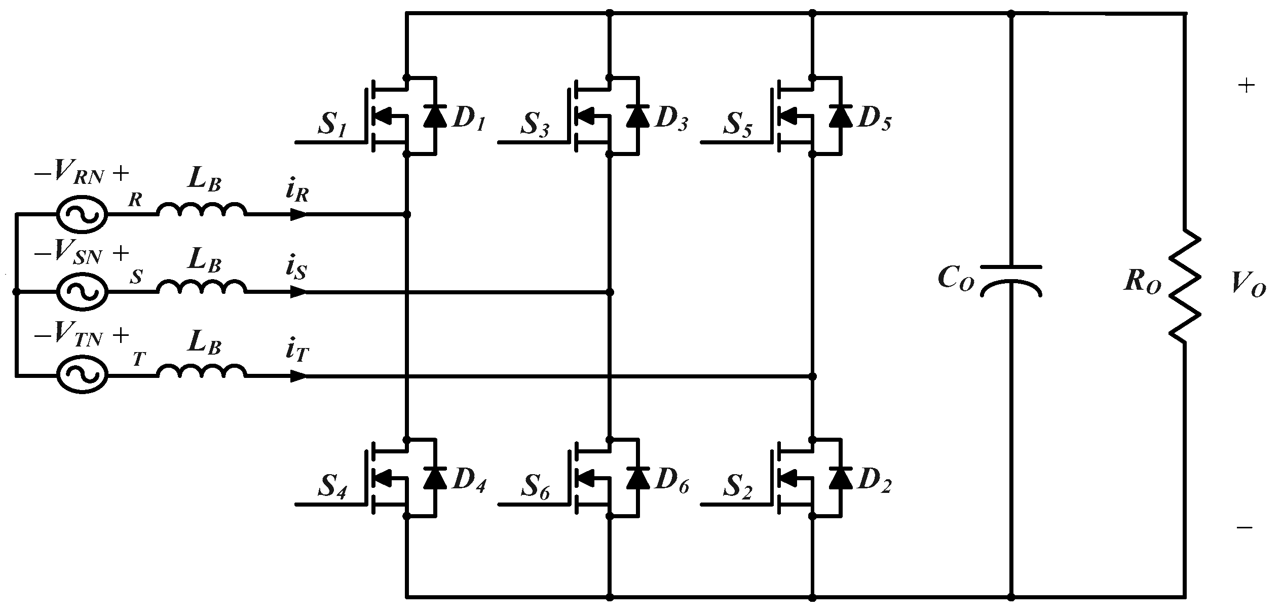
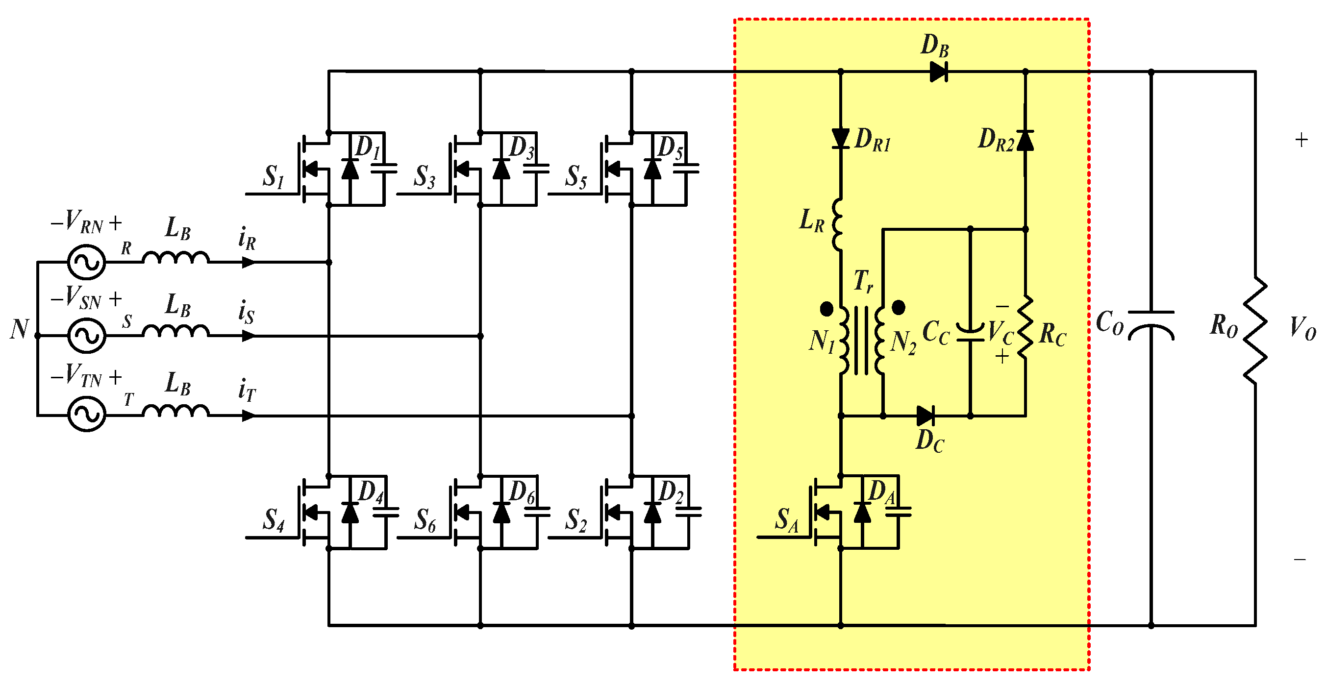
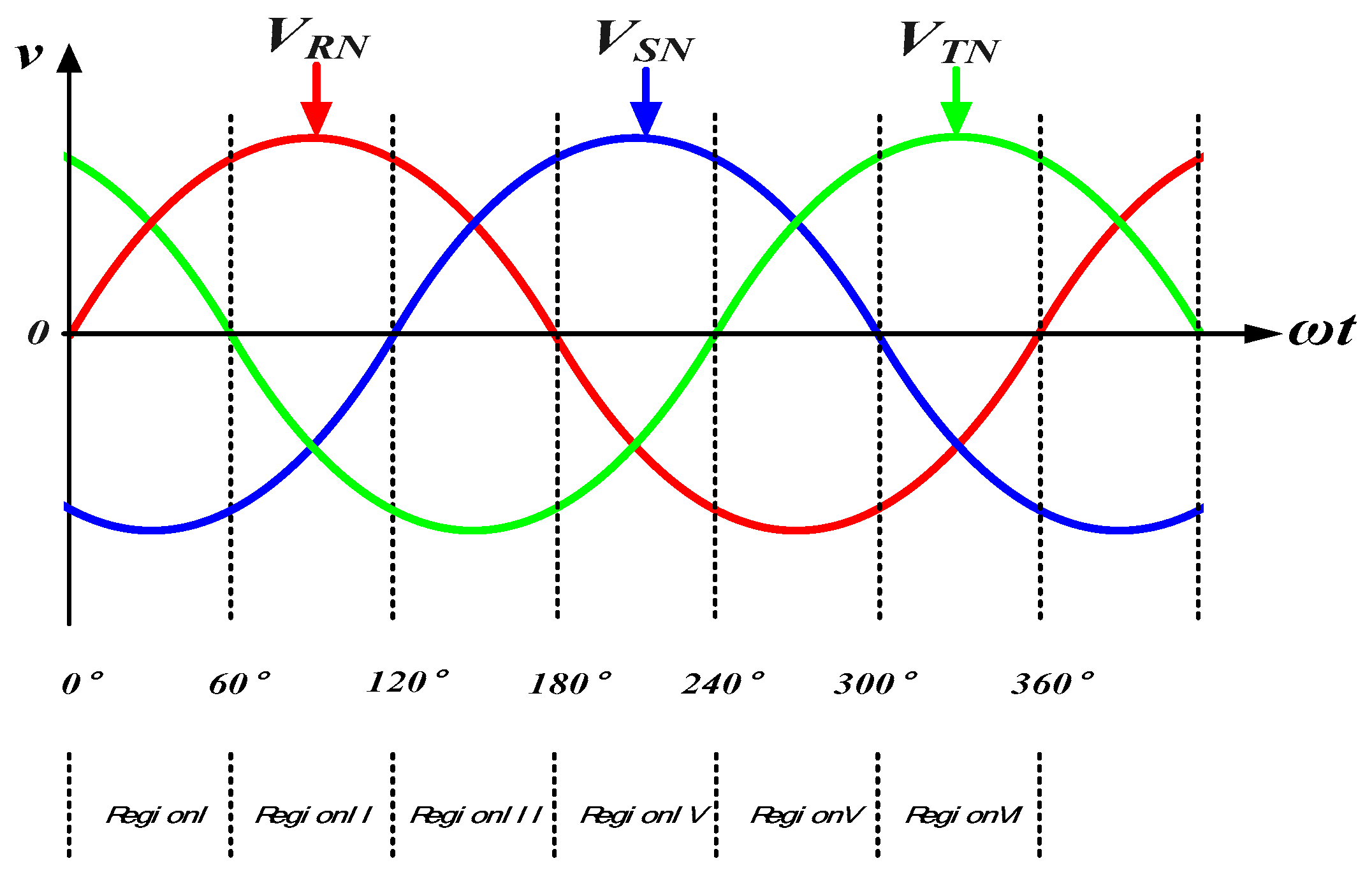
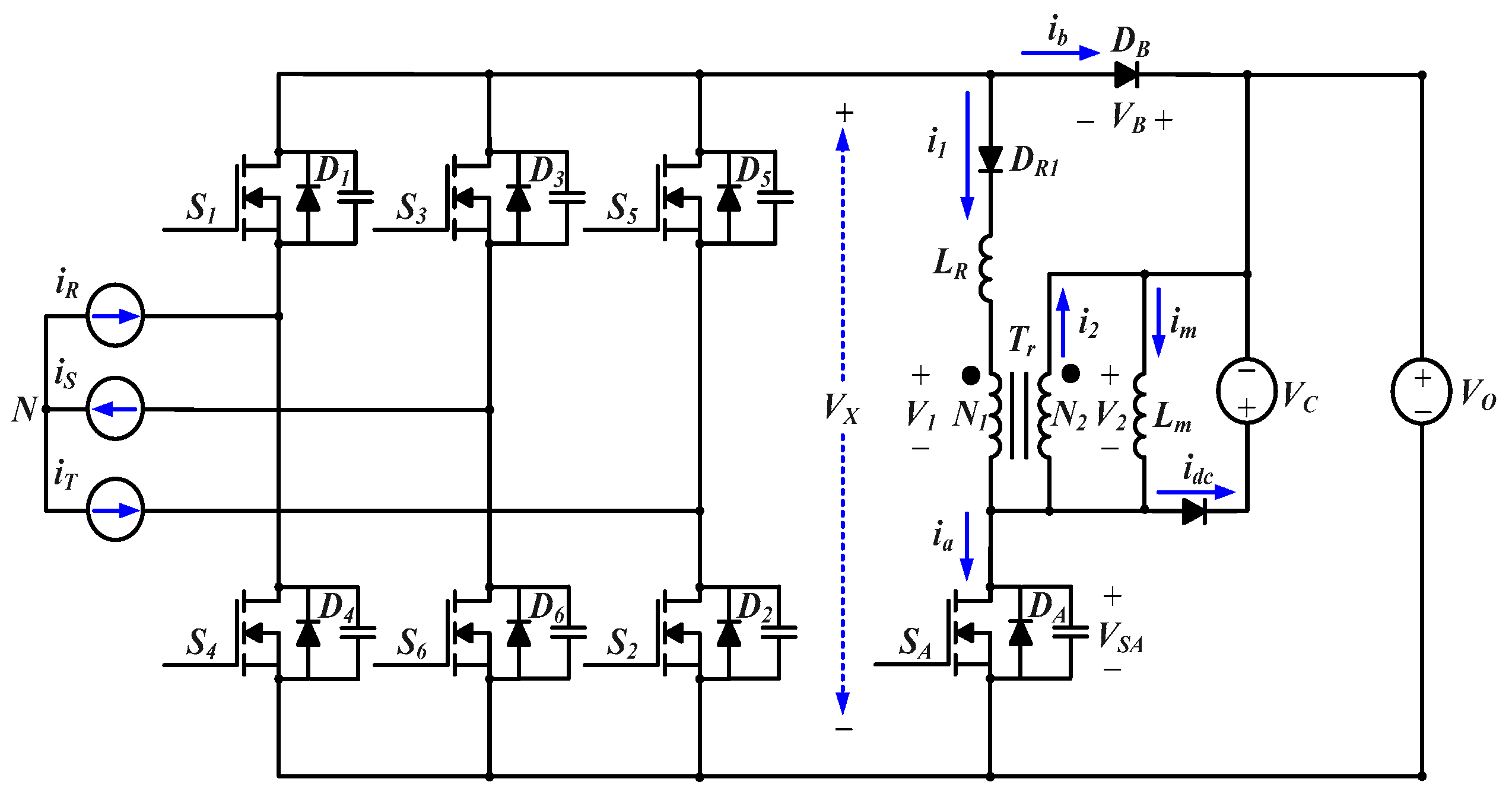
2. Proposed Three-Phase Six-Switch Soft-switching PFC Rectifier

The proposed three-phase six-switch soft-switching PFC rectifier is shown in Figure 2. The circuit inside the dotted box is a soft-switching assist circuit to achieve ZVS in the main switches and ZCS in the auxiliary switch. The soft-switching assist circuit consists of the auxiliary switch SA, resonant inductor LR, transformer Tr, barrier diode DR1, clamp circuit RC–DC–CC, and resonant capacitor (the capacitance employs the parasitic capacitance of main switch).
Three phase line voltages VRN, VSN, VTN for a balanced three-phase system are shown in Figure 3. The 60° symmetry in the three-phase voltages is evident from Figure 3. The operation of the three-phase PFC using the 60° symmetry is described in detail in [11].
In order to simplify the analysis, Interval 1 (0°–60°) can be selected for the analysis of the switching cycles as the operation over the rectifier is identical in the other 60° segments. The following assumptions are made to support the operating analysis:
(1)
Input inductance LB is large enough to allow the input current to be considered as a current source over a switching period;
(2)
Input capacitance CL is large enough to be equivalent to the ideal voltage source VO; and
(3)
The output capacitance of the clamp circuit CC is large enough to allow its voltage VC to be considered a voltage source over a switching period.
Under the assumptions listed above, the simplified circuit diagram is shown in Figure 4 and the voltage polarity and current direction for each main component are defined.
A detailed description of circuit operation is provided in this section. The key waveforms of the circuit for Interval 1 are shown in Figure 5, and equivalent circuits for each operating mode are shown in Figure 6. There are 12 operating modes to be analyzed over a switching cycle.

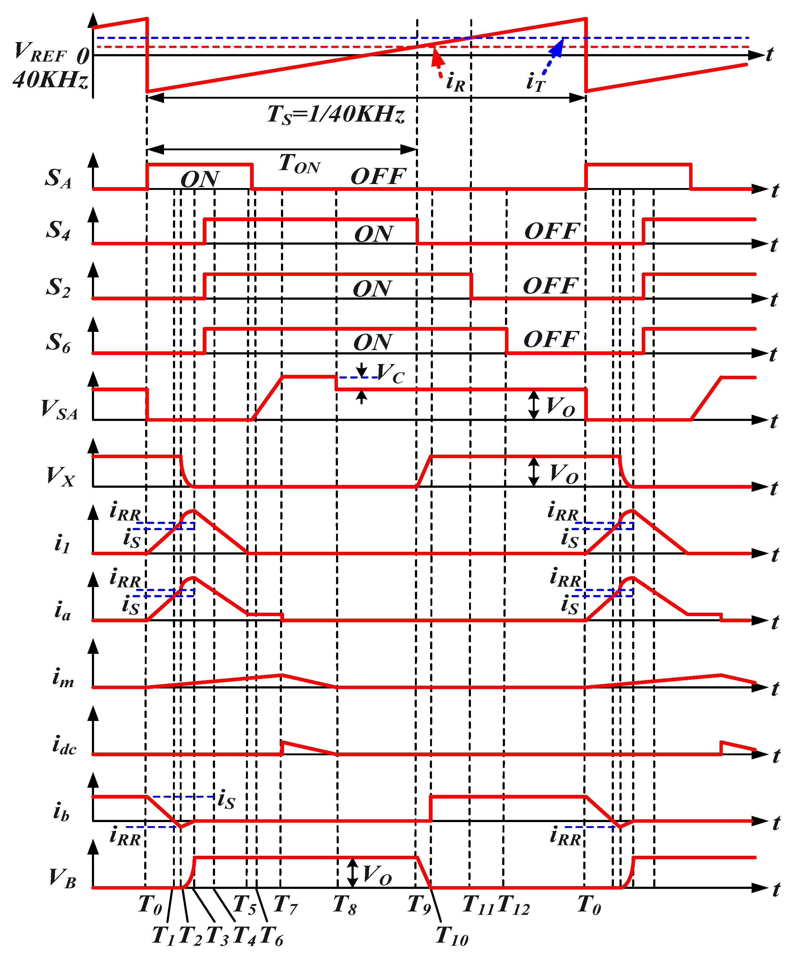
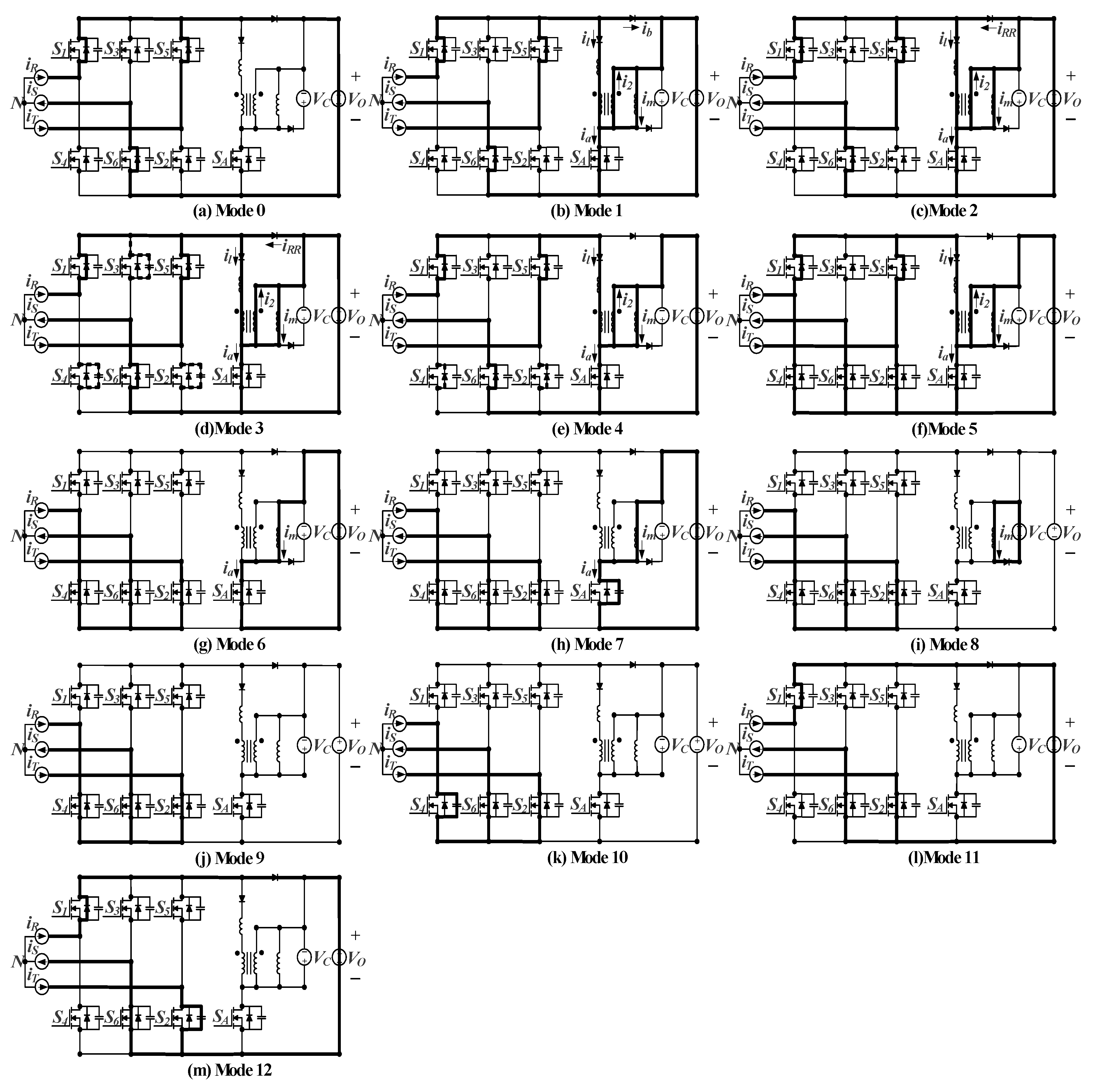
2.1. Mode 0: (t ≦ T0)

This mode is based on the analysis of the switching cycle in Interval 1 (VRN > 0, VTN > 0, and VSN < 0). Before T0, as in Figure 6a, the diode D1, D6, and D5 are in the state of conduction. The main switches S1 to S6 and auxiliary switch SA are turned off. The currents iR and iT flow through diode DB to the load and return to the AC source as the current iS. Under this condition, the voltage across the active rectifier bridge is VX = VO.

2.2. Mode 1 (T0 < t ≦ T1)

At T0, the auxiliary switch SA is turned on to go into Mode 1. The current i1 of resonant inductor LR starts to increase, and current i1 flows through the primary winding N1 of the transformer Tr. The induced current i2 and excitation current im outflow through secondary coil N2, as shown in Figure 6b. The voltage on the seconding winding N2 is the output voltage VO. The voltage V1 and V2 across the windings of transformer Tr are obtained as follows:
V 2 = V O
V 1 = N 1 N 2 V 2 = n V O
The current in the resonant inductor i1 increases linearly with the slope given by
d i 1 d t = V O V 1 L R = V O n V O L R = ( 1 n ) V O L R
Similarly to i1, the excitation current im also displays a linear increase, and the slope is
d i m d t = V O L m
When the current i1 ascends to iS current, this mode ends. The time interval is given as below:
t 01 = i s V o ( 1 n ) L R

2.3. Mode 2 (T1 < t ≦ T2)

At t = T1, the DC link diode current ib reaches zero. The reverse recovery current of diode DB flows through diode DB in a negative direction. The resonant inductor current keeps increasing, as shown in Figure 6c.

2.4. Mode 3 (T2 < t ≦ T3)

At t = T2, the parasitic capacitance of diode Db along with the resonant capacitor CR, which includes the parasitic capacitor of the main switches and the resonant inductor LR, start resonating, as shown in Figure 6d. When the equivalent voltage VX of the main switch is decreased to zero at t = T3, the mode ends. The equivalent voltage VX and resonant current i1 are shown in Equations (6) and (7).
V X = V O ( 1 n ) V O ( 1 cos ( ω R t ) )
i 1 = i s + i R R + ( 1 n ) V O Z C sin ( ω R t )
C R = C 2 + C 3 + C 4
ω R = 1 L R ( C R + C b )
Z C = L R C R + C b

2.5. Mode 4: (T3 < t ≦ T4)

When t > T3, the bridge rectifier voltage VX is decreased to zero and the auxiliary switch SA continues to conduct. The corresponding equivalent circuit is shown in Figure 6e. The body diodes D4, D3, and D2 of the main switches S4, S3, and S2 are conducting. Turning on the main switches S4, S6, and S2 when the bridge voltage reaches zero achieves ZVS turn-on. The detection circuitry to turn on the main switches at zero voltage also enables the minimization of duty-cycle loss and, thus, loss of efficiency. After the main switches turn on at ZVS, the resonant inductor current i1 decreases linearly with the slope given by Equation (11). When the current of the main switches S4 and S2 reaches zero at t = T4, the mode ends.
d i 1 d t = n V O L R

2.6. Mode 5: (T4 < t ≦ T5)

As shown in Figure 6f, when t > T4, then S4, S6, and S2 keep conducting. The current il is continuously decreased to zero until t = T5.

2.7. Mode 6: (T5 < t ≦ T6)

When t > T5, the input currents iR and iT flow through the main switches S4 and S2, as shown in Figure 6g. When the current ia flows through the auxiliary switch SA, it consists mostly of the magnetizing current, im, of the transformer. If the magnetizing inductance Lm is designed to be relatively large, the current ia of the auxiliary switch SA is extremely close to zero. When T5 < tT6, the auxiliary switch is set to be turned off so that it can effectively achieve the purpose of ZCS.

2.8. Mode 7: (T6 < t ≦ T7)

When t = T6, the auxiliary switch SA is turned off, as shown in Figure 6h. Subsequently, the magnetizing current im of the transformer charges the parasitic capacitance Coss1 of the auxiliary switch SA so that the auxiliary switch voltage will increase continuously.

2.9. Mode 8: (T7 ≦ t ≦ T8)

At t = T7, the auxiliary switch voltage VSA increases to VO + VC and the clamp diode DC is conducting. The magnetizing current im discharges through the clamp circuit DCVC, as shown in Figure 6i. The slope of the excitation current in this mode is given by
d i m d t = V C L m

2.10. Mode 10: (T8 ≦ t ≦ T9)

At t = T8, the magnetizing current im is decreased to zero which resets the transformer, as shown in Figure 6j.

2.11. Mode 10: (T9 < t ≦ T10)

At t = T9, the main switch S4 is turned off. The input current iR charges the parasitic capacitance of the main switch S4 and the equivalent voltage VX of the main switch is increased, as shown in Figure 6k.

2.12. Mode 11: (T10 ≦ t ≦ T11)

At t = T10, the equivalent voltage VX of the main switch is increased to VO and the diode DB is conducting as shown in Figure 6l. Subsequently, the antiparallel diode D1 of the main switch S1 is conducting. The input current iR flows through diodes D1 and DB and flows back from iS through the load.

2.13. Mode 12: (T11 ≦ t ≦ T12)

At t = T11, the main switch S2 is turned off. The input current iT starts to charge the parasitic capacitance of the main switch S2, as shown in Figure 6m.

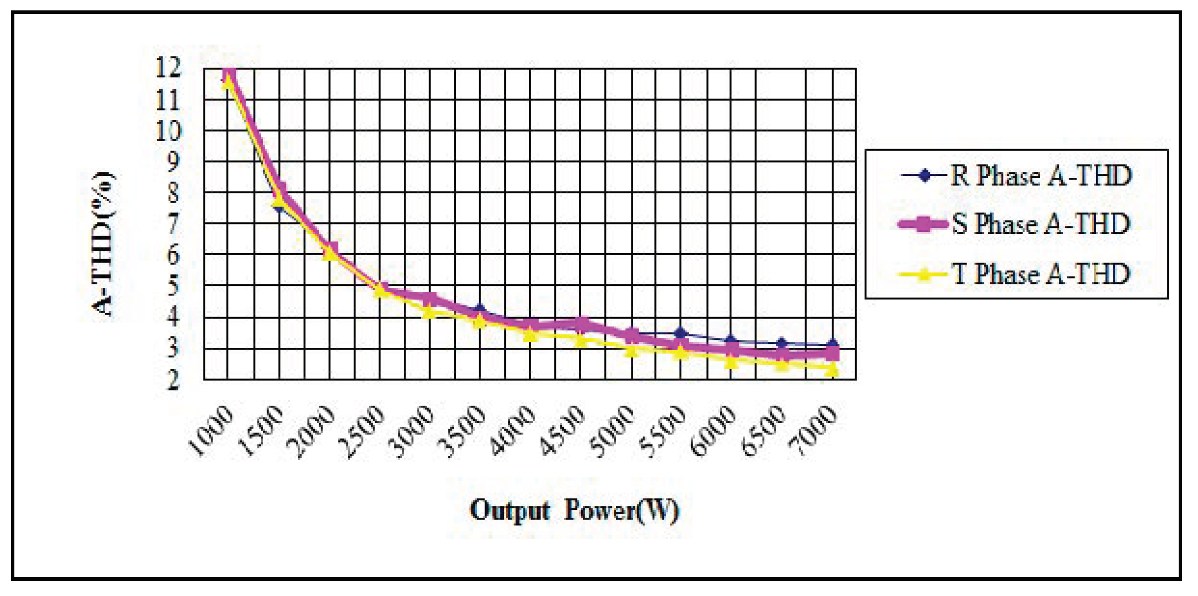
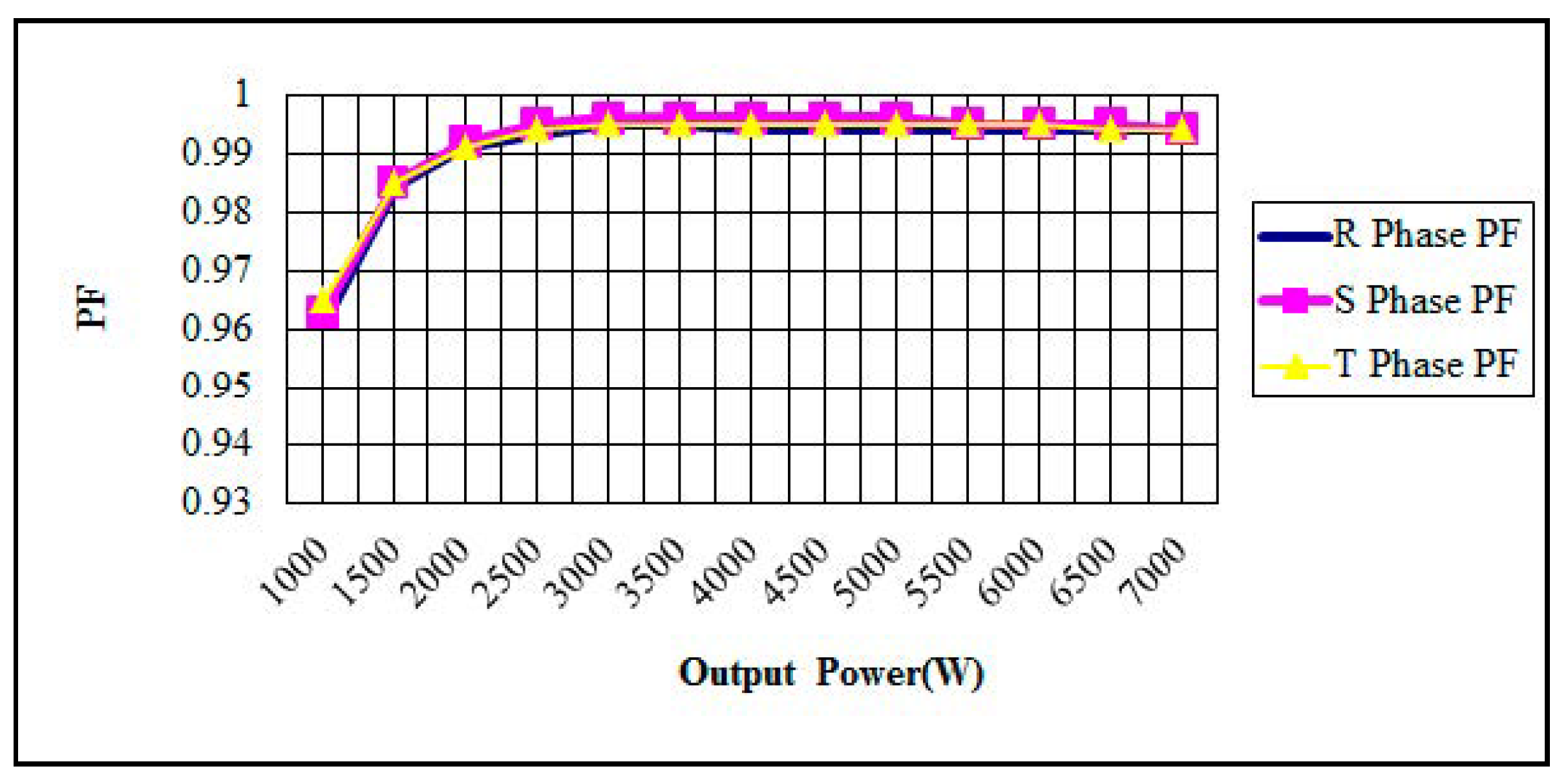
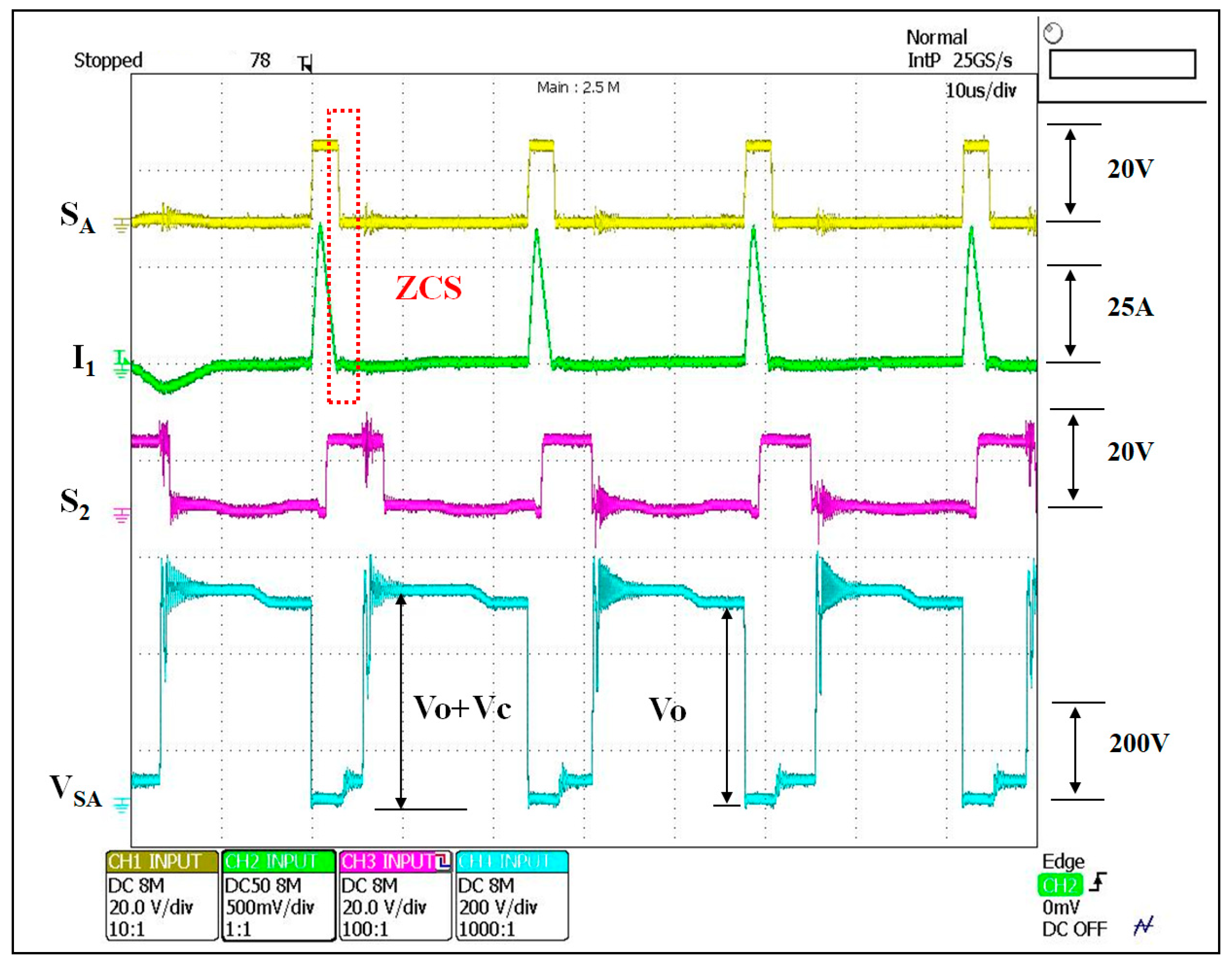
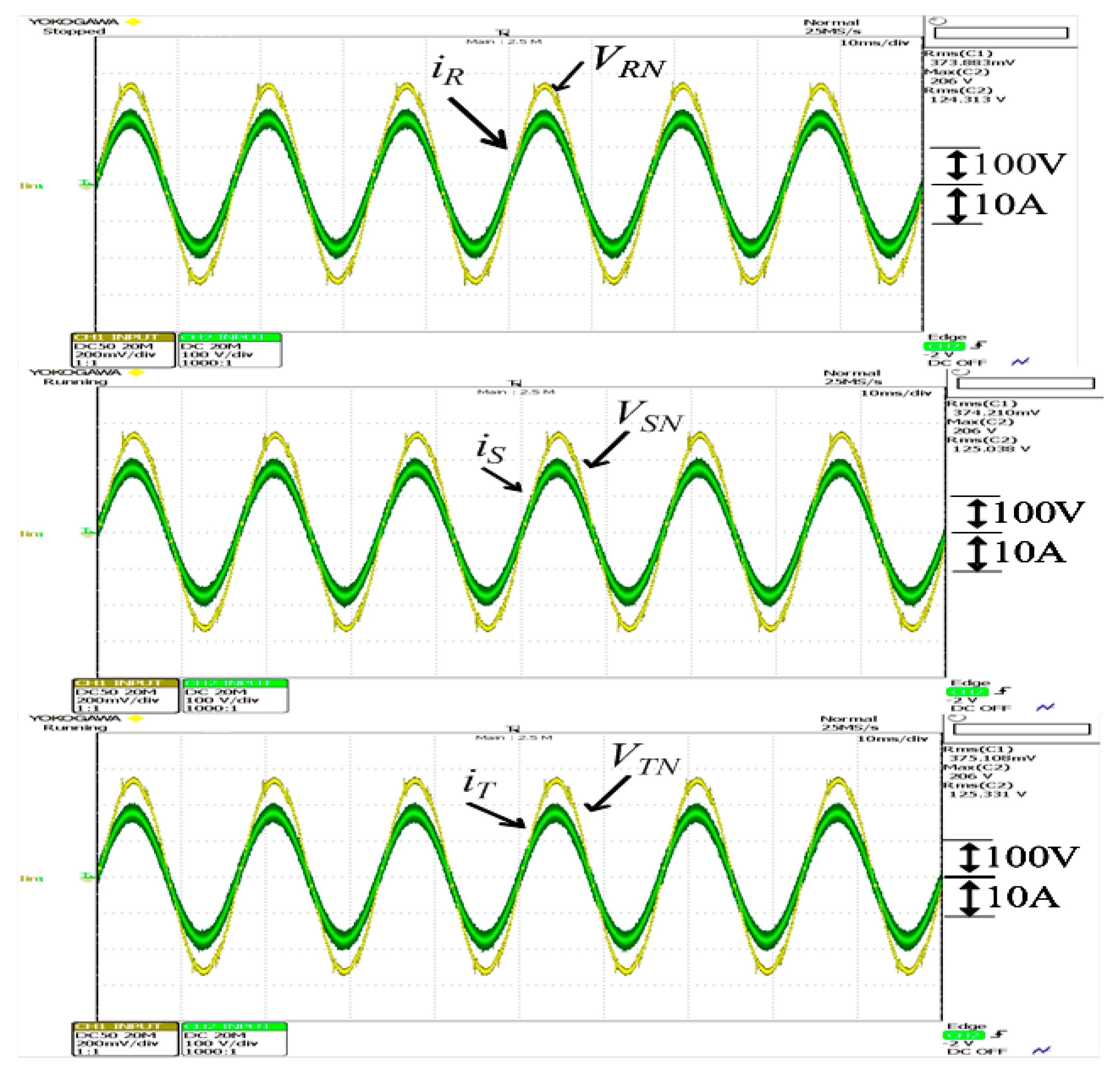
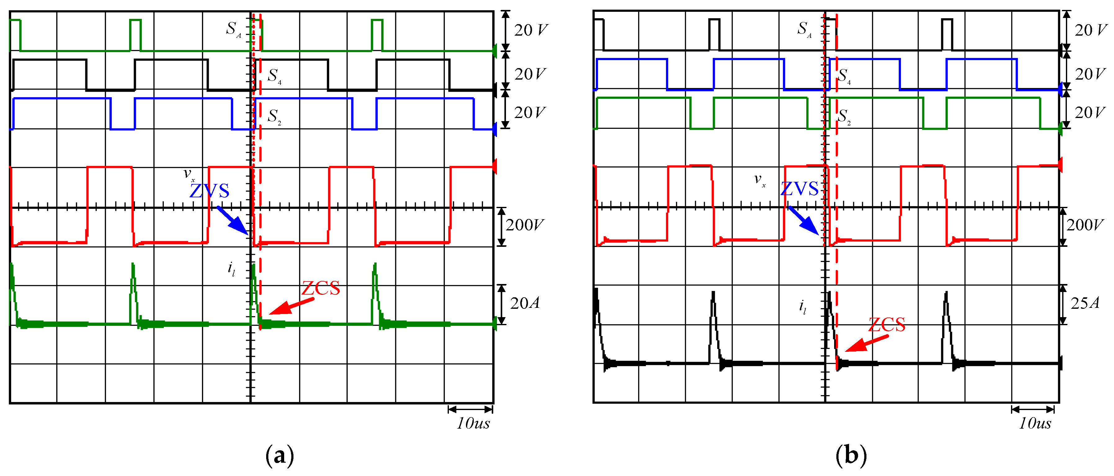
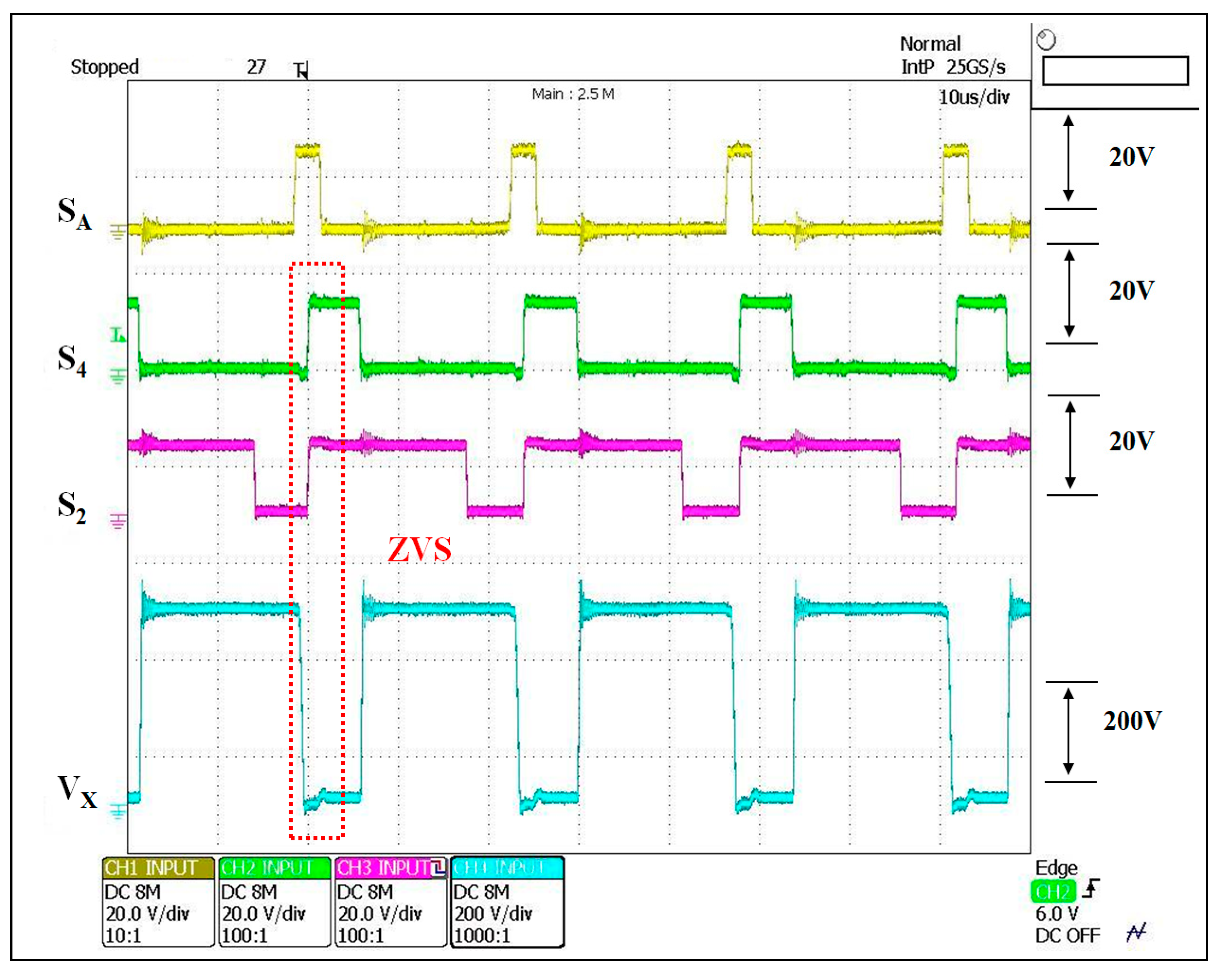
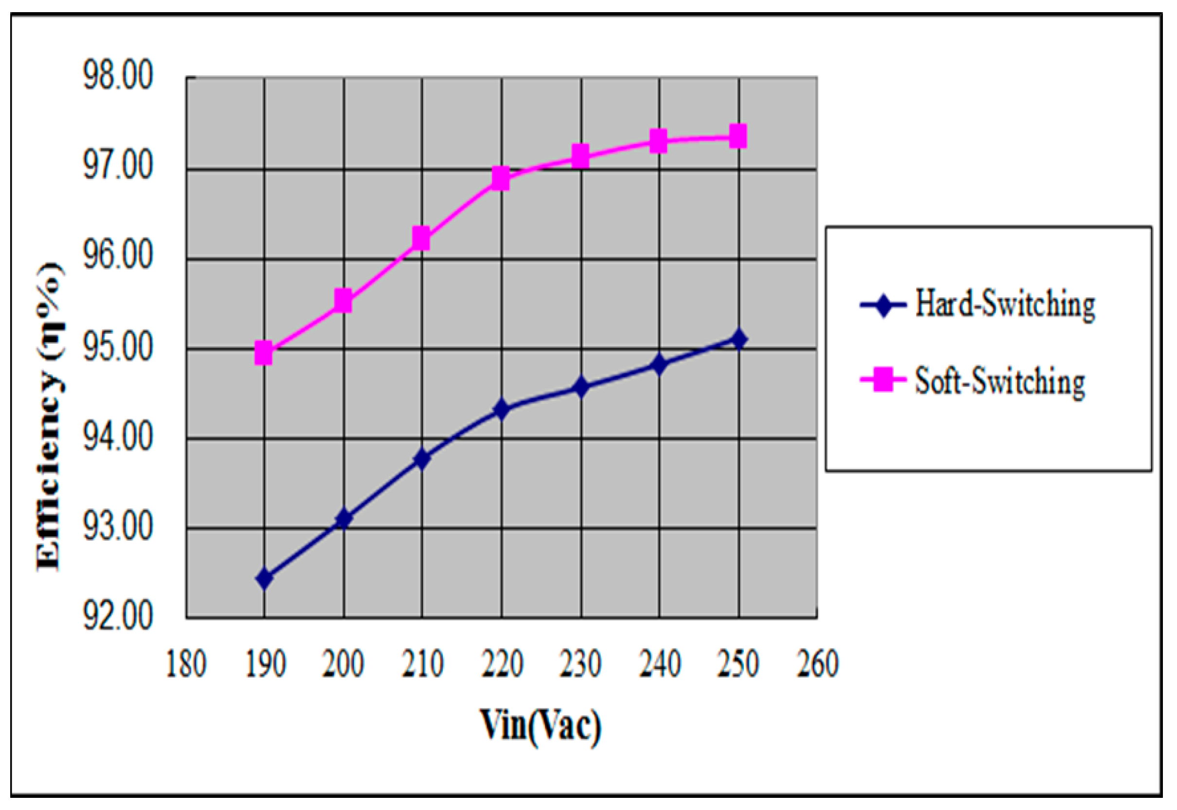
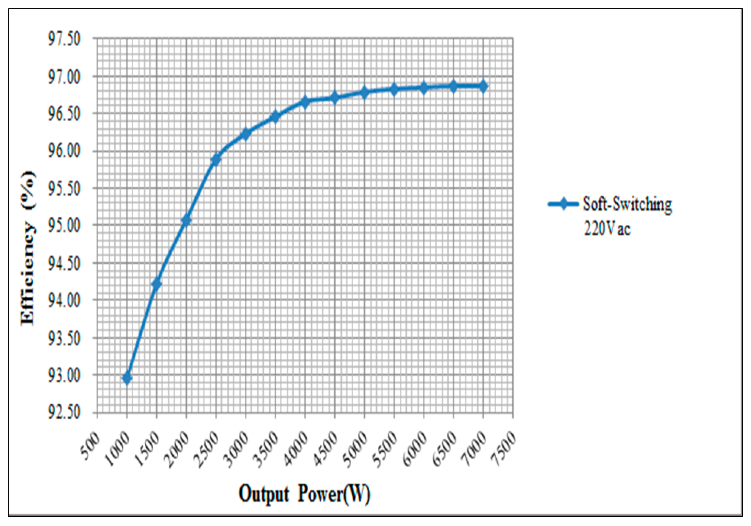
3. Experimental Verifications

Based on the design described, a prototype was built. When the line voltage in the three-phase input was 220 V, namely, the phase voltage was 127 V, the switching frequency 40 kHz, and the output load 7 kW, then the measured waveforms for three-phase VRN, VSN, VTN, line voltage and the line current were at low line and full load. The current waveform, as in Figure 7, is practically sinusoidal with low THD and a high power factor (the A-THD is shown in Figure 8 and power factor is shown in Figure 9).
Figure 10 shows the simulation waveforms using Isspice at half load and full load. It can be seen that the main switches S4 and S2 on the bottom sides turned on when their VX was down to zero by the resonant circuit, after the auxiliary switch SA was turned on.
Measured waveforms of the gate drive signals and voltage across the main switch are shown in Figure 11. The captured waveforms indicate the need to turn on the auxiliary switch SA before the turning on the main switches S4 and S2 to achieve ZVS.
As shown in Figure 12, when the current i1 of resonant inductor LR decreases to zero, the auxiliary switch SA can be turned off under ZCS conditions.
A comparison between the hard-switched and proposed soft-switched rectifier was performed at a load of 7 kW over an input voltage range of 190–250 V. The hard-switched rectifier was tested by simply disabling the soft-switch assist circuitry. Figure 13 shows the efficiency improvement from the soft-switched rectifier. The largest efficiency difference between hard-switch and soft-switch rectifier was 2.55% when the input line voltage was 220 V, and Figure 14 shows the soft-switched rectifier efficiency from 1–7 kW.

4. Conclusions

A novel three-phase rectifier with zero-voltage-switching and zero-current-switching features was proposed. The design has been validated with simulation and experimental data captured on a 7 kW three-phase rectifier prototype. Efficiency improvement between hard-switch and soft-switch rectifiers peaks at 2.55% when the input line voltage is 220 V at full load. Mathematical equations to explain circuit operation have been derived and analyzed under a sequence of operating modes. The experimental results have confirmed the proposed design of the soft-switched rectifier in achieving high efficiency, high power factor, and low THD.

Author Contributions

C.-W.L. and C.-Y.P. designed, debugged the system, built some part of hardware and performed the experiment. C.-W.L. also mainly responsible for preparing the paper. H.-J.C., supervised the design, analysis, experiment, and editing the paper.

Funding

The authors would like to acknowledge the financial support of the Ministry of Science and Technology of Taiwan through grant number NSC 103-2221-E-011 -064 -MY3.

Conflicts of Interest

The authors declare no conflict of interest.

References

  1. Ecova Plug Load Solutions Website. 80 PLUS Certified Power Supplies and Manufacturers. Available online: http://www.plugloadsolutions.com/80PlusPowerSupplies.aspx (accessed on 1 March 2019).
  2. Kolar, J.W.; Friedli, T. The essence of three-phase PFC rectifier systems—Part I. IEEE Trans. Power Electron. 2013, 28, 176–198. [Google Scholar] [CrossRef]
  3. Friedli, T.; Hartmann, M.; Kolar, J.W. The essence of three-phase PFC rectifier systems—Part II. IEEE Trans. Power Electron. 2014, 29, 543–560. [Google Scholar] [CrossRef]
  4. Chang, C.H.; Cheng, C.A.; Chang, E.C.; Cheng, H.L.; Yang, B.E. An integrated high-power-factor converter with ZVS transition. IEEE Trans. Power Electron. 2016, 31, 2362–2371. [Google Scholar] [CrossRef]
  5. Martins, M.L.S.; Hey, H.L. Self-commutated auxiliary circuit ZVT PWM converters. IEEE Trans. Power Electron. 2004, 19, 1435–1445. [Google Scholar] [CrossRef]
  6. Bodur, H.; Bakan, A.F. A new ZVT-ZCT-PWM dc/dc converter. IEEE Trans. Power Electron. 2004, 19, 676–684. [Google Scholar] [CrossRef]
  7. Ivanovic, B.; Stojiljkovic, Z. A novel active soft Switching snubber designed for boost converter. IEEE Trans. Power Electron. 2004, 19, 658–665. [Google Scholar] [CrossRef]
  8. Moran, L.; Werlinger, P.; Dixon, J.; Wallace, R. A Series active power filter which compensates current harmonics and voltage unbalance simultaneously. In Proceedings of the IEEE PESC Conference, Atlanta, GA, USA, 18–22 June 1995; pp. 222–227. [Google Scholar]
  9. Chang, Y. Boost Converter with Zero Voltage Main Switch and Zero Current Auxiliary Switches. U.S. Patent 6,498,463 B2, 24 December 2002. [Google Scholar]
  10. Tsai, H.; Hsia, T.; Chen, D. A novel soft-switching bridgeless power factor correction circuit. In Proceedings of the European Power Electronics and Applications Conference, Aalborg, Denmark, 2–5 September 2007. [Google Scholar]
  11. Jang, Y.; Jovanovic, M.M.; Fang, K.H.; Chang, Y.M. High-Power-Factor Soft-Switched Boost Converter. IEEE Trans. Power Electron. 2006, 21, 98–104. [Google Scholar] [CrossRef]
  12. Tsai, H.Y.; Hsia, T.H.; Chen, D. A Family of Zero-Voltage Transition Bridgeless Power Factor CorrectionCircuits with a Zero-Current-Switching Auxiliary Switch. IEEE Trans. Ind. Electron. 2011, 58, 1848–1855. [Google Scholar] [CrossRef]
  13. Wei, H.; Bataresh, I. Comparison of basic converter topologies for power factor correction. In Proceedings of the Southeastcon Conference, Orlando, FL, USA, 24–26 April 1998; pp. 348–353. [Google Scholar]
  14. Mohan, N.; Undeland, T.M.; Robbins, W.P. Power Electronics Converters, Applications and Design, 2nd ed.; Wiley: New York, NY, USA, 1995. [Google Scholar]
  15. Jiang, Y.; Mao, H.; Lee, F.C.; Borojevic, D. Simple high Performance three-phase boost rectifiers. In Proceedings of the IEEE Power Electronics Specialists Conference, Taipei, Taiwan, 20–25 June 1994; pp. 1158–1163. [Google Scholar]
  16. Li, R.; Ma, K.; Xu, D. A novel 40 KW ZVS-SVM controlled three-phase boost PFC converter. In Proceedings of the IEEE Applied Power Electronics Conference and Exposition, Washington, DC, USA, 15–19 February 2009; pp. 376–382. [Google Scholar]
  17. Hengchun, M.; Lee, C.Y.; Boroyevich, D.; Hiti, S. Review of high-performance three-phase power-factor correction circuits. IEEE Trans. Ind. Electron. 1997, 44, 437–446. [Google Scholar] [CrossRef]
  18. Li, Q.; Zhou, X.; Lee, F.C. A novel ZVT three-phase rectifier/inverter with reduced auxiliary switch stresses and losses. In Proceedings of the IEEE PESC PESC’96, Baveno, Italy, 23–27 June 1996; pp. 153–158. [Google Scholar]
  19. Vlatkovic, V.; Borojevic, D.; Lee, F.C.; Cuadros, C.; Gataric, S. A new zero-voltage transition, three-phase PWM rectifier/inverter circuit. In Proceedings of the IEEE PESC’93, Seattle, WA, USA, 20–24 June 1993; pp. 868–873. [Google Scholar]
  20. Kennel, R.; Schröder, D. Predictive control strategy for converters. In Proceedings of the 3rd IFAC Symposium on Control in Power Electronics and Electrical Drives, Lausanne, Switzerland, 12–14 September 1983; pp. 415–422. [Google Scholar]
  21. Mercorelli, P.; Kubasiak, N.; Liu, S. Multilevel bridge governor by using model predictive control in wavelet packets for tracking trajectories. In Proceedings of the IEEE International Conference on Robotics and Automation, New Orleans, LA, USA, 26 April–1 May 2004; pp. 4079–4084. [Google Scholar]
  22. Mercorelli, P.; Kubasiak, N.; Liu, S. Model predictive control of an electromagnetic actuator fed by multilevel PWM inverter. In Proceedings of the IEEE International Symposium on Industrial Electronics, Ajaccio, France, 4–7 May 2004; pp. 531–535. [Google Scholar]
Figure 1. A conventional three-phase six-switch power-factor-correction (PFC) rectifier.
Energies 12 01119 g001
Figure 2. The circuit of the proposed soft-switching PFC rectifier.
Energies 12 01119 g002
Figure 3. The line cycle in three-phase balance power system.
Energies 12 01119 g003
Figure 4. The simplified circuit of the proposed soft-switched rectifier.
Energies 12 01119 g004
Figure 5. The key waveforms of the proposed soft-switched rectifier.
Energies 12 01119 g005
Figure 6. Operation modes of the proposed soft-switched rectifier.
Energies 12 01119 g006
Figure 7. Measured waveforms of input voltage and input current at full load.
Energies 12 01119 g007
Figure 8. A-THD measured results.
Energies 12 01119 g008
Figure 9. Power factor measured results.
Energies 12 01119 g009
Figure 10. Simulation of key waveforms of the main switch voltage VX and current il at (a) half load and (b) full load.
Energies 12 01119 g010
Figure 11. Measured waveforms of drive signal and voltage for the main switch of the soft-switched rectifier.
Energies 12 01119 g011
Figure 12. Measured waveforms of drive signal and resonant current for the main switch of the soft-switched rectifier.
Energies 12 01119 g012
Figure 13. The efficiency comparison between hard-switching and soft-switching rectifier at 7 kW load.
Energies 12 01119 g013
Figure 14. Measured efficiency from 1 to 7 kW with the soft-switched rectifier.
Energies 12 01119 g014

