1. Introduction
The photovoltaic (PV) generation is emerging as a future energy system because of its installation convenience, no-noise, infinite, and eco-friendly characteristics [
1,
2,
3,
4]. It is classified into the centralized power system and the distributed power system depending on the scale of solar power generation [
5]. The centralized power system has a simple circuit structure with PV strings as the input energy source, but it has a disadvantage that the power generation is considerably lowered when some panels of the PV string are shaded. On the other hand, in the distributed power system, the optimal power extraction is possible because the maximum power point tracking (MPPT) control can be applied to each PV panel with a micro-inverter connected. So, it can minimize the loss of power generation caused by the shading effect. However, one micro-inverter is required for each PV panel, so implementation of this strategy is expensive. Therefore, many attempts have recently been made to lower the cost of micro-inverters.
In general, considering the cost, micro-inverters have been designed to use circuit architectures with a flyback converter [
6,
7,
8,
9,
10], which provides galvanic isolation with fewer switches than other designs. Although the flyback converter has the advantage of circuit simplicity and low cost, the design must use a transformer with a high turns ratio to achieve a high voltage-conversion ratio from low dc voltage on a single PV panel. In the transformer, the high turns ratio causes a large leakage inductance which increases the stress on semiconductor switches. Moreover, due to low utilization of the transformer, this topology is most suitable for low-power applications <200 W. Recently, multi-phase interleaved technology has been applied to solar power generation from PV panels that output ≥320 W, but this technology requires large and expensive components.
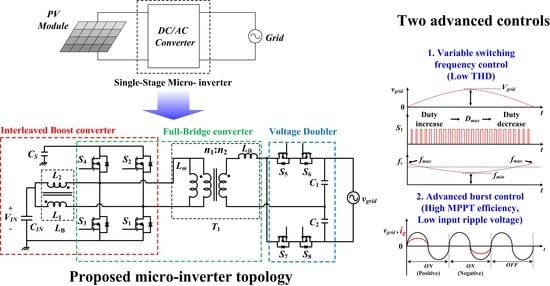
This paper proposes a low-cost, slim, single-stage micro-inverter to drive a 320-W-class PV panel. The proposed micro-inverter has an interleaved structure based on the boost half-bridge (BHB) converter [
11] with a cascaded voltage doubler. The interleaved BHB has an inversely-coupled inductor for the voltage step-up operation. The coupled inductor can reduce input ripple current and can be reduced in size. The voltage doubler increases the ac output voltage from the interleaved converter. Therefore, the transformer can have a lower turns ratio in the interleaved BHB than in a flyback converter and can be reduced in size. In the proposed micro-inverter, semiconductor switches achieve turn-on zero-voltage-switching (ZVS) and turn-off zero-current-switching (ZCS) by exploiting the resonance between the leakage inductance of the transformer and output capacitors of the voltage doubler, without additional components.
This paper also presents two advanced control algorithms. First, a variable switching frequency control scheme was implemented to reduce total harmonic distortion (THD) by reducing output ripple current. Then an advanced burst control scheme was implemented to improve power-conversion efficiency at light loads. By distributing output current temporally at light loads, input ripple voltage can be reduced. Therefore, the size of decoupling capacitors is reduced and MPPT efficiency is improved compared with the conventional burst control [
12,
13].
Section 2 describes the circuit structure and operating principles of the proposed micro-inverter,
Section 3 gives the proposed control schemes,
Section 4 shows experimental results using a 320-W prototype micro-inverter, and
Section 5 concludes the paper.
2. Circuit Structure and Operating Principles of the Proposed Micro-inverter
The proposed micro-inverter (
Figure 1) consists of an interleaved boost converter, a full-bridge converter, and a voltage doubler. The portion that is composed of the interleaved boost and full-bridge converters is based on a boost half-bridge topology. The interleaved boost converter consists of an inversely-coupled inductor
LB, four switches
S1–
S4, and a storage capacitor
CS. The full-bridge converter consists of a transformer
T1 and the same four switches
S1–
S4 as the interleaved boost converter. The voltage doubler has four switches
S5–
S8 and two capacitors
C1 and
C2.
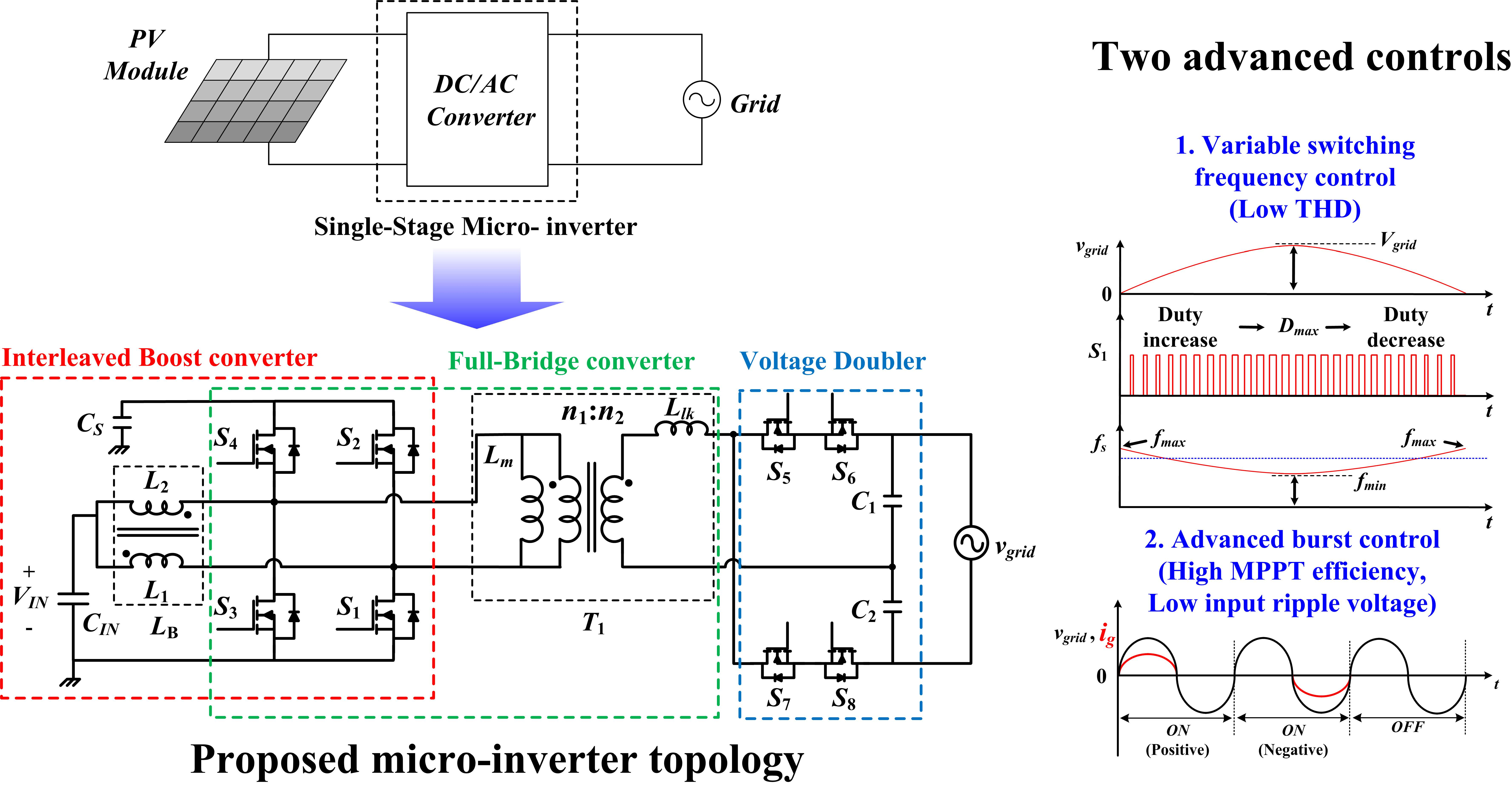
In the proposed interleaved boost converter, two inductors
L1 and
L2 form
LB (
Figure 2) by using a single magnetic core instead of two separate magnetic cores used in the conventional interleaved boost converter [
14].
LB has a turns ratio of 1:1;
L1 and
L2 each have self-inductance
L. The mutual inductance
M between
L1 and
L2 is represented as:
where
k is the coupling coefficient. The voltage drops of
L1 and
L2 are given, respectively, by
and
Using Equations (2) and (3) and
yields
and
S1, the body diode of
S2, and
L1 form one boost power stage.
S3, the body diode of
S4 and
L2 form the other boost power stage. The two boost power stages form an interleaved boost converter and two outputs operate out of phase. When
S1 or
S3 is turned on, voltage
is applied to
L1 or
L2, respectively. When
S1 or
S3 is turned off, voltage
is applied to
L1 or
L2, respectively. The energy accumulated during the on-state for each boost power stage is transferred into
CS. There are four cases of the voltage
v1 of
L1 and the voltage
v2 of
L2 depending on the states of
S1 and
S3. Using Equations (4) and (5), the equivalent inductance for each case is obtained (
Table 1).
M < 0 in Equation (1), so
Table 1 demonstrates that appropriate design of the inversely coupled inductor can reduce the input ripple current of the micro-inverter [
15].
The full-bridge converter shares four switches S1–S4 with the interleaved boost converter, and its input power comes from CS. The leakage inductance Llk of T1 and capacitors C1 and C2 in the voltage doubler form an LC resonant circuit. The LC resonant current flows through the primary and secondary sides of T1 with turns ratio n1:n2. This current causes the body diode of each switch to conduct before the turn-on gate signal is applied, thus achieving zero-voltage-switching (ZVS) for S1–S4.
In the voltage doubler, S5–S8 rectify current on the secondary side of T1. When grid voltage is positive, both S5 and S8 are turned on, and both S6 and S7 act as diodes. When grid voltage is negative, both S6 and S7 are turned on, and both S5 and S8 act as diodes. The energy transferred to the voltage doubler through T1 is stored in C1 and C2. C1 and C2 are connected in series, and the output voltage of the micro-inverter is the sum of the voltage vC1 of C1 and the voltage vC2 of C2.
In the proposed micro-inverter, variable-switching-frequency control is used, and the output voltage is a sinusoidal grid voltage. However, for simplicity, the analysis is based on the assumption that the micro-inverter generates a constant output voltage with a fixed switching frequency at a certain point in the analysis. In addition, the electrical losses of all components are ignored, and the following conditions are assumed: and , where Lm is the magnetizing inductance and Ts is the switching period. The operation cycle S1–S4 is the same regardless of the polarity of the grid voltage, so the analysis considers only positive grid voltage.
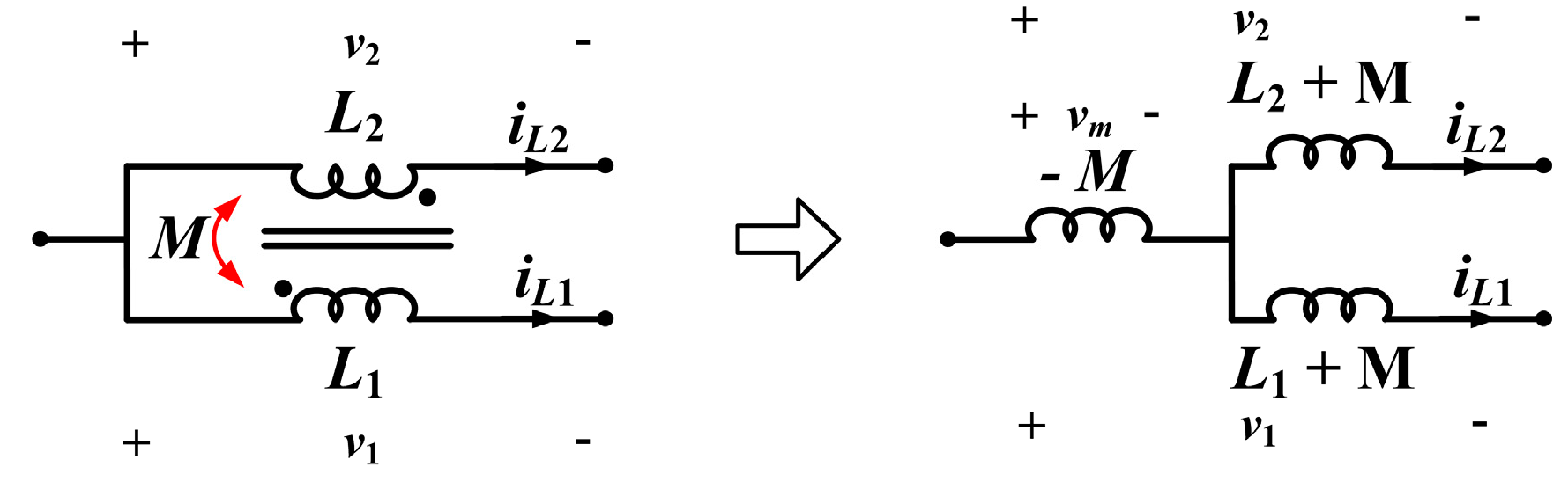
The operating waveforms (
Figure 3) of the proposed micro-inverter depend on the duty ratio
D. First, operational states are analyzed for
D ≤ 0.5 (
Figure 3a and
Figure 4).
State 1 (
t0–
t1): At
t =
t0,
S1 is turned on,
vDS1 = 0, and
iSW1 < 0.
S4 remains in the turn-on state, and both
S2 and
S3 remain in the turn-off state. For
T1, the voltage
vLm across
Lm is equal to
vCs, and the secondary voltage
vs proportional to the turns ratio
n1:
n2 is generated on the secondary side of
T1. The magnetizing current
iLm is increased and is given by:
Resonance is generated by
Llk on the secondary side of
T1 and capacitors
C1 and
C2, and the state equation is given by
Using Equations (7) and (8), the secondary current
is of
T1 is obtained as
where
is the resonant impedance and
is the resonant angular frequency.
From Equations (6) and (9), the primary current
ip of
T1 is obtained as
From
Table 1, the currents
iL1 and
iL2 of the coupled inductor are obtained as
State 2 (t1–t2): At t = t1, S1 is turned off and S4 remains in the turn-on state. Both S2 and S3 remain in the turn-off state. This interval is a dead time to prevent shoot-through before S2 is turned on. During this state, the drain-source voltage of S1 increases from 0 V to vCs and that of S2 decreases from vCs to 0 V by charging and discharging parallel capacitance across each switch, respectively.
State 3 (
t2–
t3): At
t =
t2,
S2 is turned on,
vDS2 = 0, and
iSW2 < 0.
S4 remains in the turn-on state, and both
S1 and
S3 remain in the turn-off state. For
T1, the voltage
vLm across
Lm is 0 V and the voltage
vlk across
Llk is –
vC1. The amplitude of
iLm remains unchanged during state 3 as:
is begins to decrease because the energy stored in
Llk is transferred to
C1, and is given by
From Equations (14) and (15),
ip is obtained as
From
Table 1,
iL1 and
iL2 are obtained as
State 4 (t3–t4): At t = t3, S4 is turned off and S2 remains in the turn-on state. Both S1 and S3 remain in the turn-off state. This time interval is a dead time to prevent shoot-through before S3 is turned on. During this state, the drain-source voltage of S4 increases from 0 V to vCs and that of S3 decreases from vCs to 0 V.
The proposed micro-inverter has an interleaved structure, so both the operating principle of the next half cycle for D ≤ 0.5 and the operating principle for D > 0.5 are the same as the above analysis except for the switches used. Thus, further analysis for the others is not given.
The voltage gain
Gv of the proposed micro-inverter is twice the product of the boost converter voltage gain and the full bridge converter voltage gain:
3. The Proposed Control Schemes
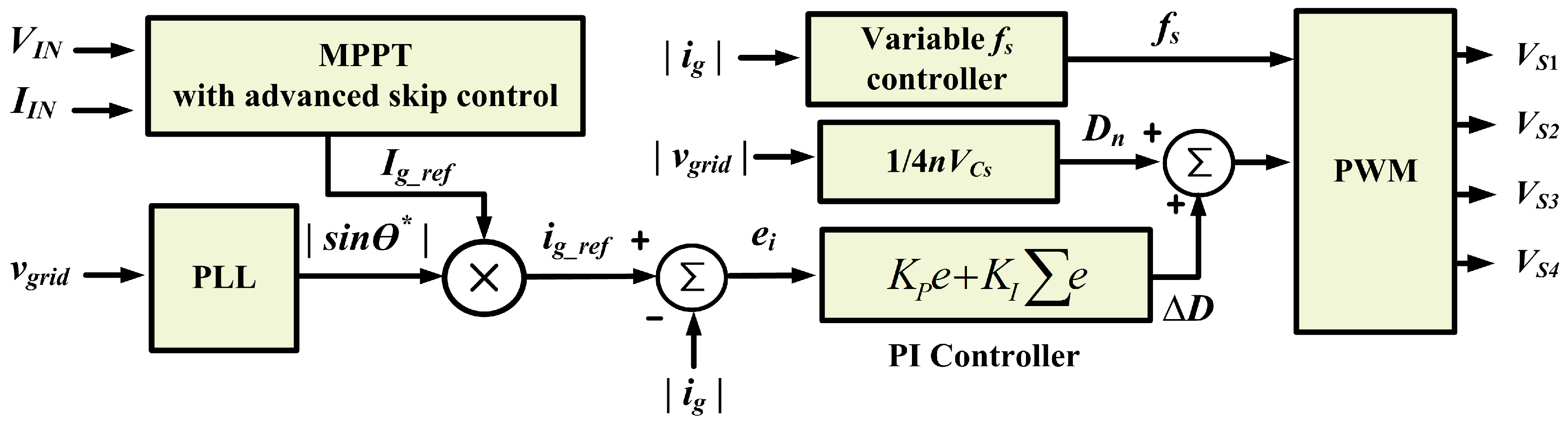
The main controller (
Figure 5) for the proposed micro-inverter takes as analog-to-digital inputs the grid voltage
vgrid, the grid current
ig, the input voltage
VIN and the input current
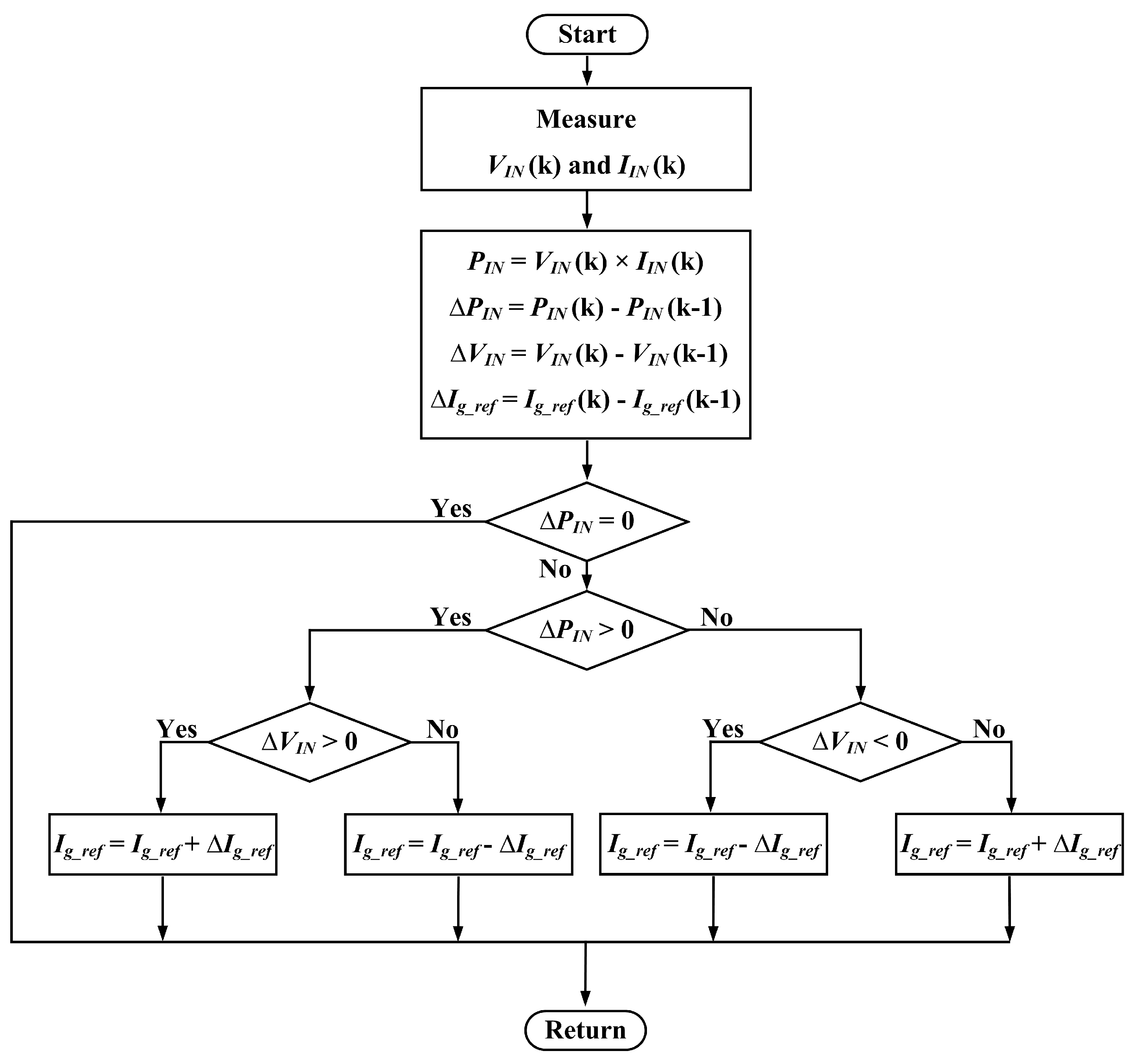
IIN. The MPPT controller is based on the perturb and observe (P&O) MPPT algorithm [
16]. This controller determines the amplitude of the reference grid current
Ig_ref by using
IIN and
VIN to maximize solar power generation. In the P&O MPPT algorithm used (
Figure 6),
Ig_ref is increased if Δ
PIN > 0 and Δ
VIN > 0 or if Δ
PIN < 0 and Δ
VIN < 0.
Ig_ref is decreased if Δ
PIN > 0 and Δ
VIN < 0 or if Δ
PIN < 0 and Δ
VIN > 0. This process is repeated until the maximum power point (MPP) is reached, i.e., Δ
PIN = 0.
The phase-locked loop (PLL) generates the phase information |
sin θ*| by using
vgrid. In the PLL, virtual voltage
vq1 is derived from
vgrid for phase detection.
where
GPLL(s) is PLL gain and
Vgrid is the amplitude of
vgrid.
From the inverse Laplace transform of
vq1(s),
where
ωt is the actual phase of the grid.
Using equation (20), the other virtual voltage
vq2 is obtained as
vgrid and
vq2 are transformed into the synchronous reference frame as follows:
where
θ* is a phase output from the PLL. From Equation (22),
The PLL generates
θ* to follow ωt through PI control inside the PLL. The reference current signal
ig_ref is the product of
Ig_ref and |
sin θ*|:
The proportional-integral (PI) controller determines the duty ratio variation Δ
D by using the difference between
ig_ref and |
ig| as follows:
Δ
D compensates for the voltage drop of
Llk, so that
ig follows
ig_ref. The nominal duty ratio
provides stable system dynamics for nonlinear sinusoidal waves which are difficult to control using only Δ
D. The total duty ratio
where
Dn is duty ratio generated by the grid voltage and Δ
D is a duty ratio variation generated by the grid current.
D is given to the pulse-width-modulation (PWM) controller. The PWM controller generates gate signals for switches to track the reference power.
Operating modes (
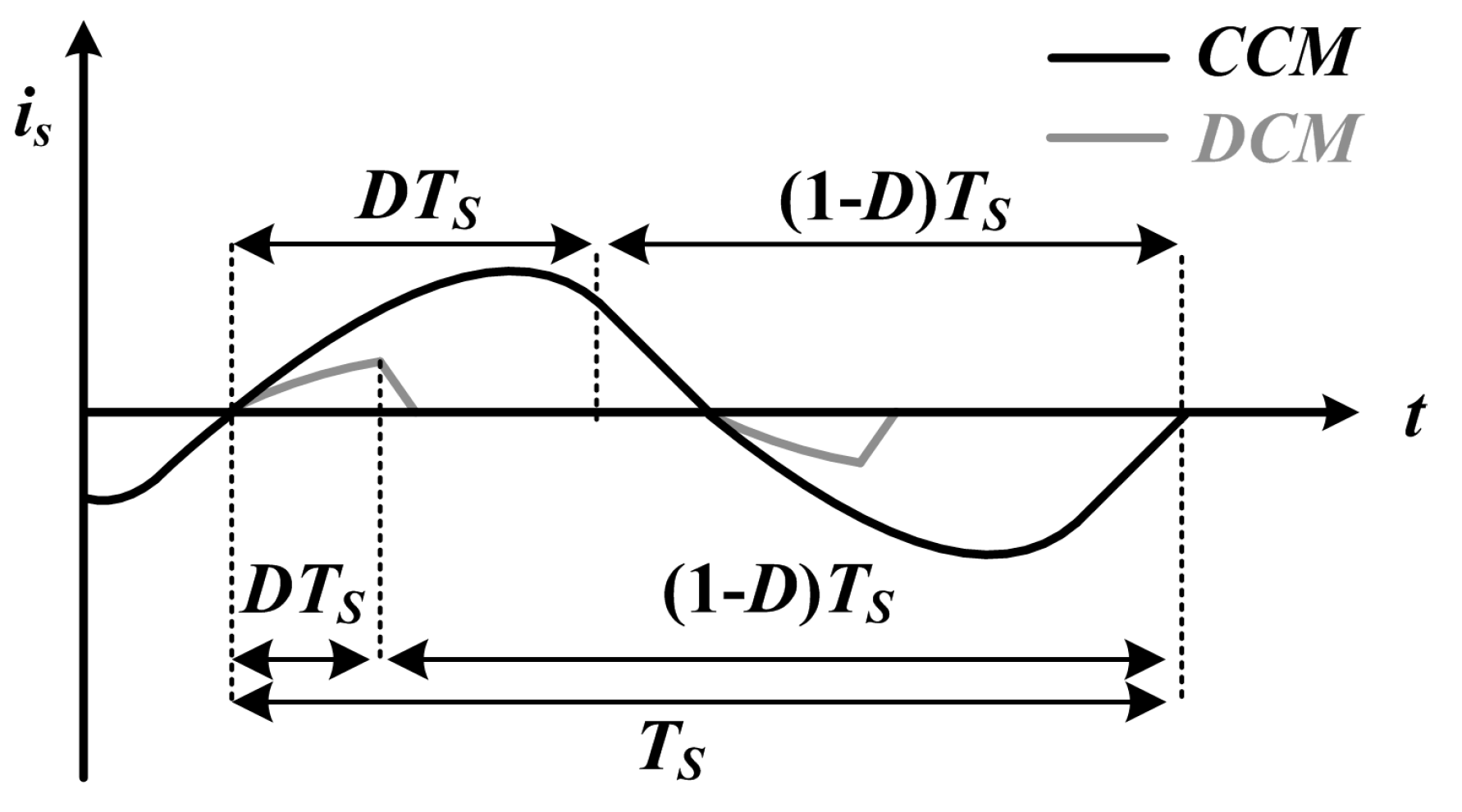
Figure 7) depend on the grid current level when grid voltage is positive. When
ig is low, the proposed micro-inverter operates in discontinuous conduction mode (DCM) because
ig becomes zero before the end of the switching cycle with the period
Ts. When
ig is high, continuous conduction mode (CCM) is applied.
If a fixed switching frequency is used for the operating modes, especially the DCM mode, two problems occur: (1) High grid current ripples at low grid currents increase total harmonic distortion (THD); (2) as the output power decreases, the total DCM operating time can increase over the total CCM operating time, and the power conversion efficiency of the micro-inverter can be reduced by high current stress. To solve these problems, this paper proposes two advanced control schemes: Variable-switching-frequency (VSF) control and the advanced burst (AB) control.
3.1. Variable Switching Frequency Control
During
Ts,
is of
T1 in DCM and CCM modes vary with
D (
Figure 8). As
D decreases, the energy stored in
Llk decreases, so time required to demagnetize
Llk decreases. Therefore, the micro-inverter is operated in DCM mode. From Equations (9) and (15), the operating condition for DCM is given by
Existing methods to optimize the DCM mode duration have drawbacks. One method is to increase the value of Llk; a large Llk increases the inductive energy and increases the demagnetizing time, but this solution requires a large transformer with a large number of windings. Another solution is to increase the switching frequency fs; this approach can also increase the power density, but high fs causes high switching loss. Thus, this paper presents VSF control, which minimizes switching loss without increasing the transformer size. VSF control varies fs depending on the magnitude |ig| of the grid current.
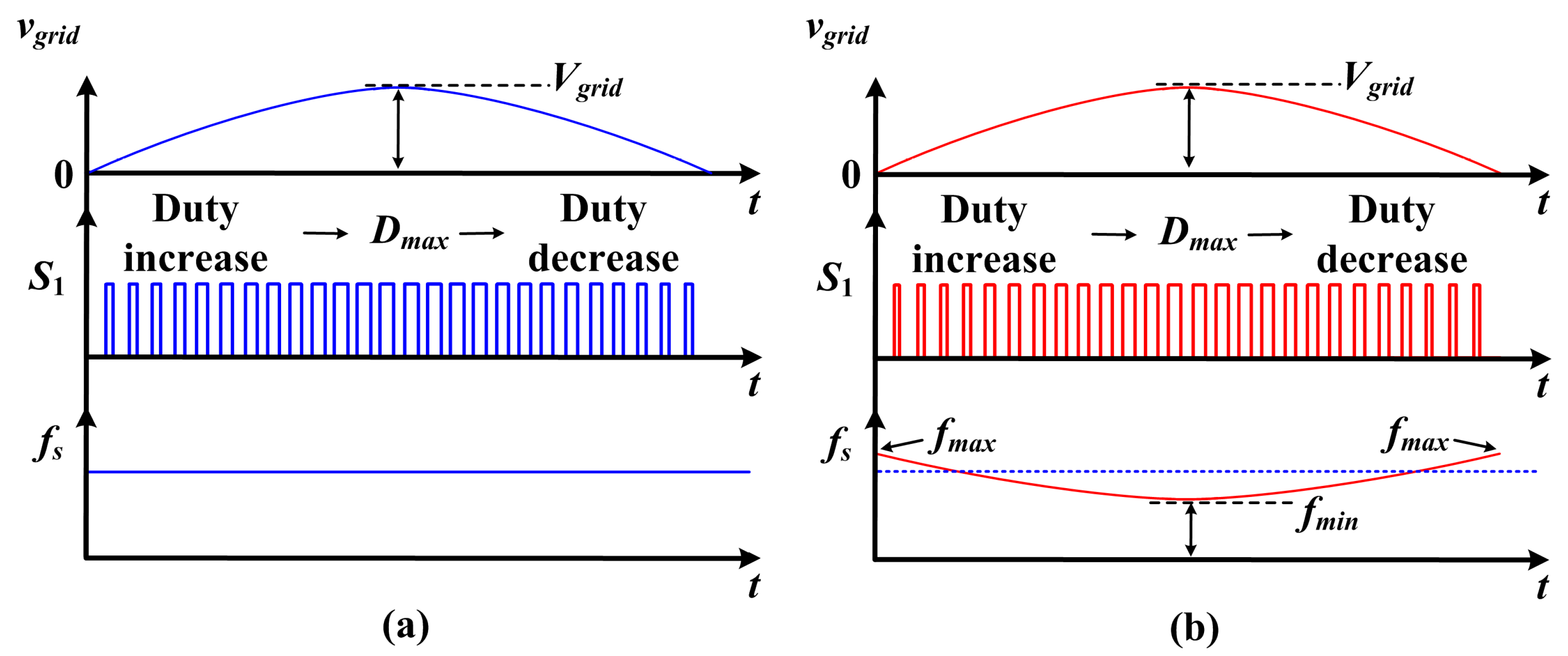
Fixed-switching-frequency (FSF) control and VSF controls have distinct attributes (
Figure 9). FSF control changes only
D depending on
vgrid (
Figure 9a). In contrast, VSF control changes both
D and
fs depending on
vgrid (
Figure 9b). When
vgrid is near zero, the switching loss is very small because
ig is close to zero. Therefore, when VSF control is used,
fs is increased to the maximum switching frequency
fmax and the time interval between demagnetizings of L
lk is reduced (
Figure 9b). As
vgrid increases,
fs is decreased to the minimum switching frequency
fmin to reduce switching losses.
fs is given by
where
Vgrid is the peak value of
vgrid. 3.2. Advanced Burst Control
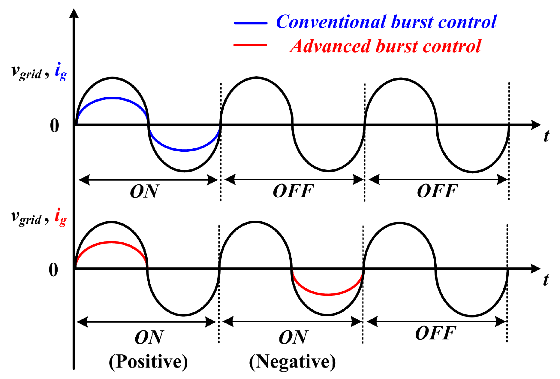
When solar power generation and load are very small, micro-inverters operate only intermittently to supply the desired power to the grid on an average power basis. This intermittent operation is called “burst control”. For the burst control, the micro-inverter supplies ig to the grid only during the ON state, and stops running during the OFF state. The burst control improves power-conversion efficiency by reducing the ripple of ig and switching loss when the load is small.
In the conventional burst control scheme, positive and negative grid currents are consecutively supplied to the grid during one ON-state period (
Figure 10). Then OFF-state periods follow the ON-state period. During the OFF state, no power is output, so output occurs only during the ON state, and the energy flowing out of
CIN is also concentrated. Therefore, the input ripple voltage Δ
VIN is increased, the MPPT efficiency is reduced, and additional time is required to charge the input capacitor
CIN for the next operation.
To further improve the performance of burst control, this paper proposes AB control, which supplies positive grid current during the first ON-state (
Figure 10). The negative grid current is supplied during the ON-state that immediately follows the first ON-state period. Then, OFF-state periods follow the ON-state periods. This scheme has the effect of distributing the output current temporally compared with the conventional burst control scheme. Therefore, in the proposed micro-inverter with the advanced burst control scheme, the MPPT efficiency can be improved, and the input capacitance
CIN can be reduced due to the reduced Δ
VIN.
4. Experimental Results
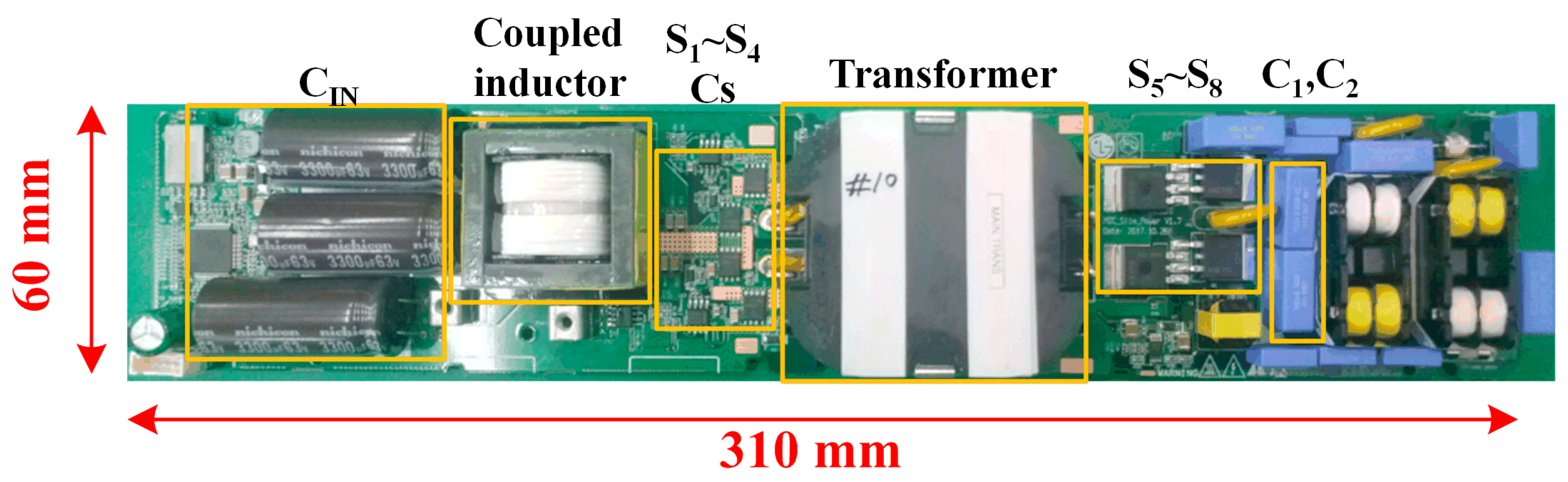
The proposed grid-connected micro-inverter (
Figure 11) was designed to operate at the rated power 320 W,
VIN = 25~52 V
DC,
IIN.max = 12 A
DC, and
fs = 60~90 kHz. The grid voltage was 220 V
rms, the grid frequency was 60 Hz, and grid current supplied by the proposed micro-inverter is 0~1.45 A
rms. The proposed micro-inverter was implemented using the circuit parameters given in
Table 2. The microcontroller used was a MN103DF35 (PANASONIC). For the PI controller in the main controller,
KP and
KI were experimentally optimized and set to 9.5 and 200, respectively. The sampling frequency for analog signals is 20 kHz, and the resolution of the analog-to-digital converter is 12 bits. The turns ratio of
LB is 10:10 and that of
T1 is 6:19. The resonant frequency
fr = 35.5 kHz from
Llk = 100 µH and
C1 =
C2 = 100 nF. The MOSFET package of
S1–
S4 is PG-TDSON-8 and that of
S5–
S8 is D
2PAK. Capacitors
Cs,
C1 and
C2 are MPP-film type. The fabricated micro-inverter was compact and slim with 60-mm width, 310-mm length, and 30-mm height.
Instead of an actual PV module, the photovoltaic simulator ETS600X14CPVF TerraSAS from AMETEK was used as an input source. The solar cell I-V characteristic curve for the experiment was based on that of the NeON®2 PV module from LG electronics.
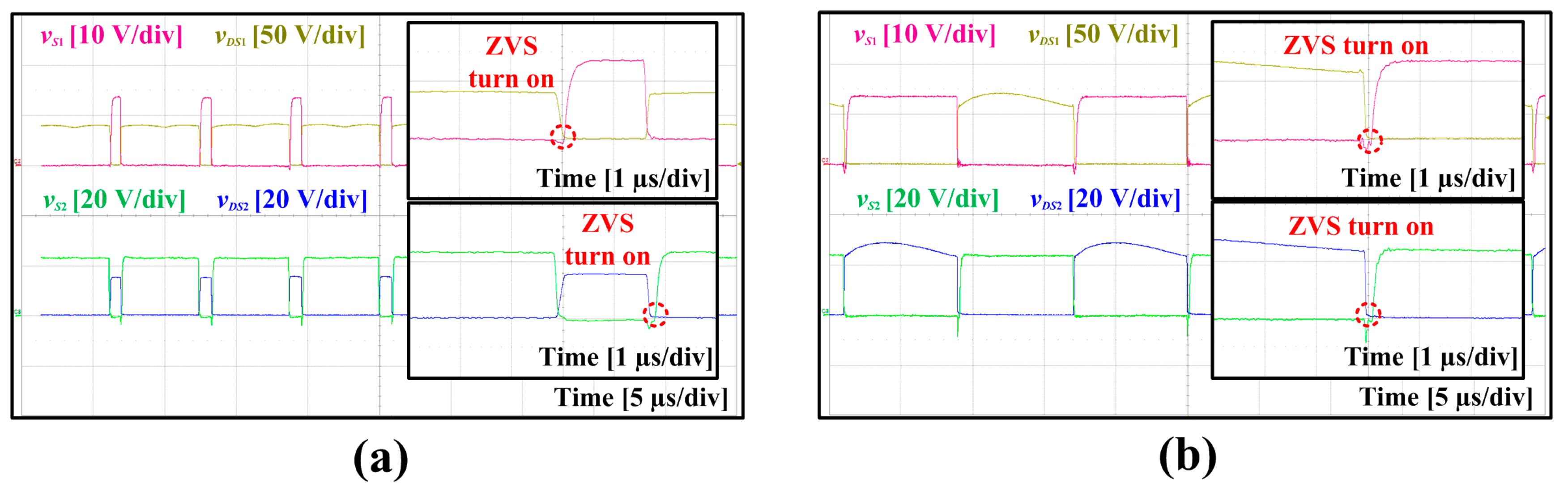
Gate-source and drain-source voltages were obtained for
S1 and
S2 at
D ≤ 0.5 (
Figure 12a) and at
D > 0.5 (
Figure 12b) at
VIN = 34 V and
vgrid = 220 V
rms /60 Hz. The drain-source voltage v
DS1 of
S1 drops to 0 V before the gate signal
vS1 is applied, so
S1 turns on with ZVS.
S2 is complementary to
S1 and achieves a ZVS turn-on. The operation of
S3 and
S4 is out of phase with that of
S1 and
S2, so
S3 and
S4 can also achieve the ZVS turn-on.
Waveforms (
Figure 13) were obtained for
vgrid and
ig at
VIN = 34 V and
vgrid = 220V
rms / 60 Hz for output power
Po = 320 W and 64 W. To maximize efficiency, the proposed micro-inverter operates in normal mode at
Po ≥ 110 W and in AB control mode at
Po < 110 W. The boundary of the output power at which the proposed micro-inverter switches from the normal mode to AB control mode and vice versa is selected to be in a range where the peak value of
ig does not exceed the rated grid current.
Waveforms were obtained for the fixed-frequency (
Figure 14a) and the variable-switching-frequency (
Figure 14b) controls. Gate signals of
S1 and
S3,
ig and
vgrid were measured at
VIN = 34 V,
vgrid = 220 V
rms / 60 Hz, and output power
Po = 320 W. When fixed-switching frequency control was used,
ig was distorted near zero-crossing, and THD was increased to 5.79%. In contrast, when variable switching frequency control was used, the distortion of
ig was improved near zero-crossing, and THD was reduced to 2.65%, which is below the requirement for distributed power. The switching frequency
fs decreased as
ig increased, so switching loss was also reduced.
Δ
VIN is higher when conventional burst control is used (
Figure 15a) than when AB control is used (
Figure 15b), because AB control reduces the energy supplied by
CIN during one ON-state period. At
VIN = 34 V,
vgrid = 220 V
rms / 60 Hz, and
Po = 32 W, Δ
VIN was 4.2 V when conventional burst control was used, but 2.4 V when AB control was used.
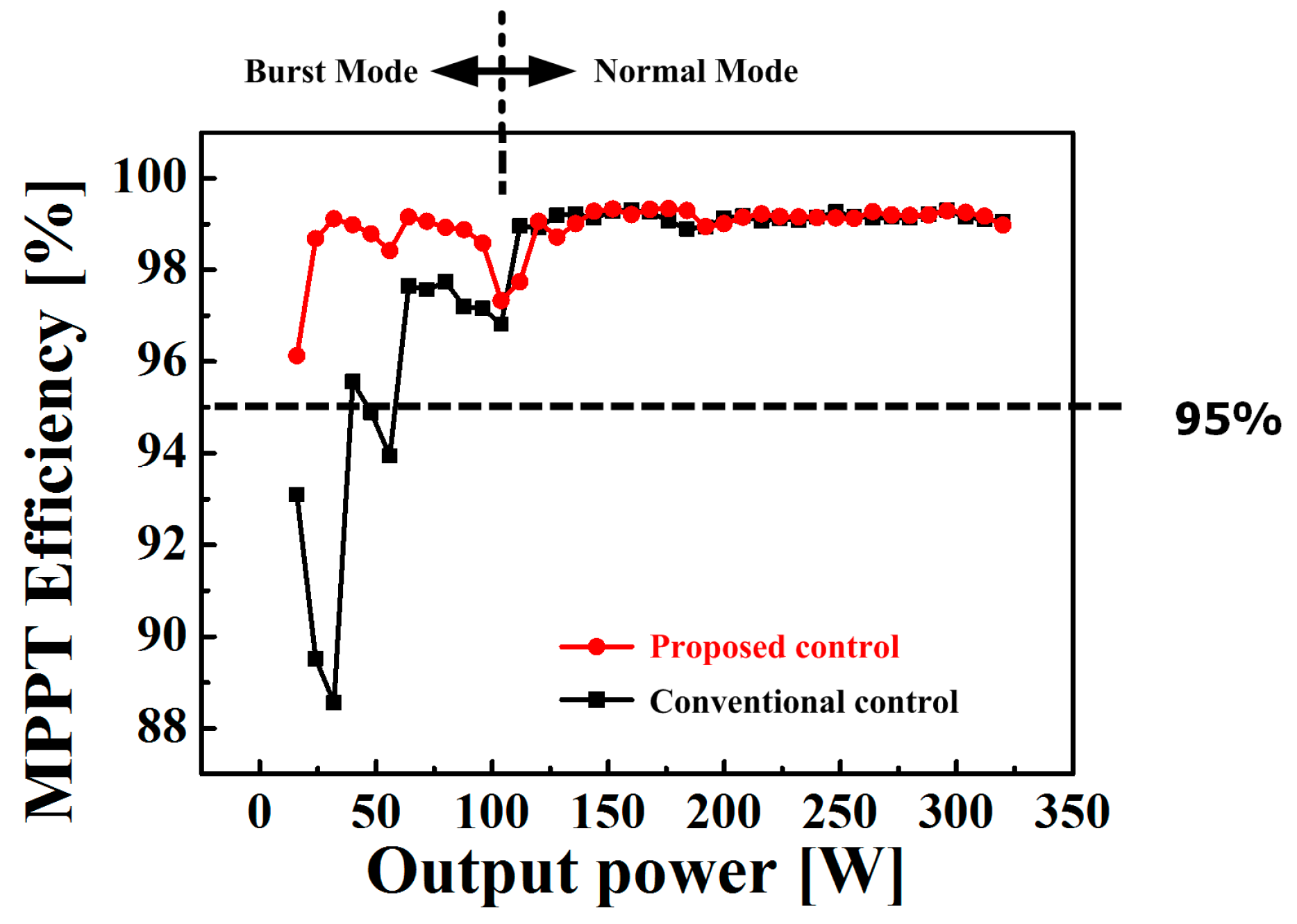
The MPPT efficiency of the proposed micro-inverter was measured (
Figure 16) in the range of irradiance from 50 W/m
2 (
Po = 16 W)–1000 W/m
2 (
Po = 320 W). In the proposed control scheme, for
Po < 110 W (burst mode), the MPPT efficiency was kept >95% because Δ
VIN and Δ
Ig_ref are reduced. However, in the conventional control scheme, the MPPT efficiency was reduced to ~88% because fluctuation of
Ig_ref increased. During burst mode, the maximum MPPT efficiency was >99% for the proposed control scheme but <97.5% for the conventional control scheme.
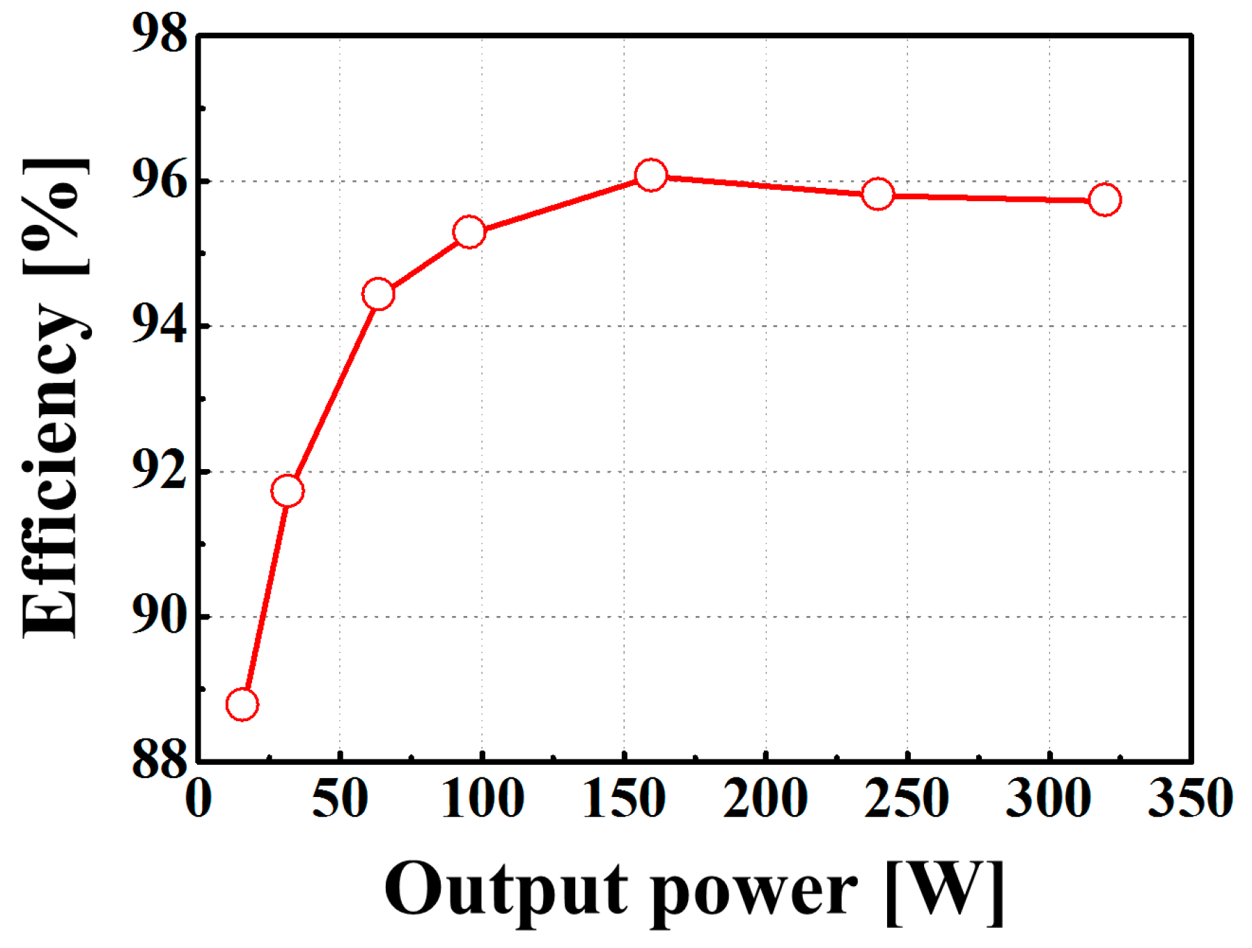
In a micro-inverter, one of the most important factors is the power conversion efficiency ɳ
e for 50~75% load under actual solar irradiation. Therefore, the California Energy Commission (CEC) weighted efficiency to represent this fact has been widely used to measure the performance of micro-inverters. The power conversion efficiency ɳ
e (
Figure 17) was measured for the proposed micro-inverter; the result indicate that the CEC weighted efficiency [
17,
18] is 95.55%, in which ɳ
e(10%) = 91.71%, ɳ
e(20%) = 94.42%, ɳ
e(30%) = 95.28%, ɳ
e(50%) = 96.06%, ɳ
e(75%) = 95.8%, and ɳ
e(100%) = 95.72%. The maximum ɳ
e is 96.06% for
Po = 160 W.


