Article

Experimental Investigation on the Performances of a Multilevel Inverter Using a Field Programmable Gate Array-Based Control System

Dipartimento di Ingegneria, Università degli Studi di Palermo,Viale delle Scienze, 90128 Palermo, Italy
*
Author to whom correspondence should be addressed.
Energies 2019, 12(6), 1016; https://doi.org/10.3390/en12061016
Submission received: 1 February 2019 / Revised: 9 March 2019 / Accepted: 12 March 2019 / Published: 15 March 2019
(This article belongs to the Section F: Electrical Engineering)

Abstract

:
The Field Programmable Gate Array (FPGA) represents a valid solution for the design of control systems for inverters adopted in many industry applications, because of both its high flexibility of use and its high-performance with respect to other types of digital controllers. In this context, this paper presents an experimental investigation on the harmonic content of the voltages produced by a three-phase, five level cascaded H-Bridge Multilevel inverter with an FPGA-based control board, aiming also to evaluate the performance of the FPGA through the implementation of the main common modulation techniques and the comparison between simulation and experimental results. The control algorithms are implemented by means of the VHDL programming language. The output voltage waveforms, which have been obtained by applying to the inverter the main PWM techniques, are compared in terms of THD%. Simulation and experimental results are analyzed, compared and finally discussed.

1. Introduction

Over the last decades, the technological advances of software for the implementation of digital systems, which are generally finalized to the control of specific applications, has significantly contributed to the simplification of the design processes of digital controllers dedicated for the electrical energy conversion [1]. The Digital Signal Processor (DSP) is a very wide-spread digital controller that allows the implementation of control algorithms through a purely software programming (C or C++). The related hardware, even if composed by several peripherals (e.g., the RAM or the ROM), presents an already designed structure and, therefore, the flexibility of use of the microcontroller is significantly reduced.
The Field Programmable Gate Array (FPGA) is another example of digital controller composed by a matrix of Configurable Logic Blocks (CLBs) with completely reprogrammable connections. Thus, if compared with a DSP, the FPGA ensures a higher flexibility, even if the complexity of the system in the low-level programming is challenging. Moreover, the previously mentioned feature allows the realization of a system of logic operations developed in parallel, reducing the computing time and leading to the achievement of high-performance control systems, which can be even compared with equivalent controllers composed by analogical components [2,3,4,5]. Nevertheless, it has to be highlighted that the adoption of a DSP could generally provide a much faster software development with respect to a FPGA. However, according to [1,2,6], the latter can overcome to some of the major disadvantages of the conventional microprocessor or DSP controls. In fact, as aforementioned, one of the main advantages is the independence between the architecture of the device and the written code. Furthermore, the hardware can be reconfigured in a very easy manner [2].
Moreover, in comparison with Complex Programmable Logic Devices (CPLDs), the adoption of an FPGA allows the design of very complex digital systems, providing higher flexibility with a lower design security and allowing the adoption of Computer-Aided Design (CAD) [1,5].
Several papers in the literature have focused their attention in the field of multilevel converters controlled by FPGA, especially for high-speed control systems [7,8,9,10,11,12,13,14,15,16,17,18]. For instance, Islam et al. [8], as well as Zhou et al. [9], proposed the modeling and experimental evaluation of multilevel inverters control, focusing their interest towards the implementation through FPGA and not on the harmonic content of the voltage waveform for the different modulation techniques. Similar analysis and experimental results are given in [10,11,12], but for different cases of applications. In addition, Aime et al. [13] proposed the use of a FPGA for the Peak Current Control (PCC) in a multilevel inverter: the main tasks of the FPGA architecture, such as ramp generation, dead time creation, switching orders generation, voltage regulation, are well described. Gateau et al. [14] highlight the role of FPGA in the implementation of a digital sliding-mode observer of the flying capacitors in stacked multicell converters (SMCs). Nevertheless, the potential benefits in terms of THD improvement are not extensively proven.
In [15], Coppola et al. presented an FPGA-based control strategy for Cascade Half Bridge (CHB) inverters: despite a wide exploitation of the FPGA tasks (e.g., Maximum Power Point Tracking, MPPT, and sorting algorithm implementation, dead time generation, measurement stage) the FPGA system is not responsible for the PWM control, which is implemented by a DSP. Moreover, the work described in [16] takes into account only three modulation techniques, also referring several DSP disadvantages such as the increased processing time or a reduced accuracy due to the limited available resources. Mentions of the flexibility of the FPGA system in terms of industry applications can be found in [17,18,19,20,21,22]. In particular recent papers [17,18,20] address the control of modular multilevel converters, and others face the growing application on electrical mobility from battery management systems [19] and traction [21,22,23]. All proposed recent papers report FPGA as the best answer for implementing in real time the control techniques, due to its adaptive parallel processing hardware structure, which permits implementing diverse algorithms with reducing the serial and consecutive operations compared to traditional CPU implementation.
In this context, this paper aims to present a detailed investigation and experimental validation on the performances in terms of harmonic distortion of the voltages produced by a cascade h-bridge multilevel inverter, defined in Section 2, controlled by an FPGA and for several modulation techniques. The harmonic content is evaluated by means of the approximate total harmonic distortion parameter, which is defined in Section 5.
Moreover, in the field of the DC-AC conversion systems, multilevel converters, with respect to the traditional ones, provide great advantages such as lower Total Harmonic Distortion (THD) of the waveforms, lower strains to both load and switches and reduction of the issues related to the electromagnetic compatibility. However, the main drawbacks for these converters can be identified in a higher overall cost of the device and a higher complexity for the design of control and command circuits.
Multilevel converters are commonly used for medium voltage/high power applications, as reported in [24]. Furthermore, the use of components with high switching frequencies and low losses (i.e., power MOSFET) allows the multilevel converters to be applied also for low-power and low voltage applications, as reported in [25,26].
In comparison with multilevel converters of the traditional type, higher number of levels can be obtained through particular structures reported in [27,28,29].
Generally, due to the complex structure of the multilevel inverters, several studies have been carried out in order to reduce the number of components. For instance, Jamaludin et al. [30] proposed the use of bidirectional switches with an auxiliary circuit in order to reduce the complexity of a three-phase full-bridge inverter. A hybrid circuital structure was proposed by Gautam et al. [31], in which the number of controlled switches, diodes and DC sources is considerably reduced. Another innovative topology for medium/high voltage is presented in [32], consisting of a series-connected symmetric module and a three-phase inverter. However, the reduction of the number of components leads to a reduction on its flexibility of use and, therefore, innovative control techniques must be developed [33].
In this context, the aim of this paper is to present an experimental investigation of the main Multicarrier Pulse Width Modulation (MC PWM) techniques for a three-phase, five level cascaded H-bridge inverter by means of a FPGA controller-based board, which represents a favorable solution for the design of control systems for inverters, mainly due to its high flexibility of use.
In the first step, the analysis is carried out in order to compare the simulation and experimental results of the proposed techniques. For this purpose, the Total Harmonic Distortion (THD%) is used as a parameter for comparison. Then, the analysis is focused on two cases of study, in order to experimentally investigate on the harmonic content of the voltage waveforms, deeply describing the steps of the low-level programming with FPGA implementation. Finally, this extensive analysis is also validated by means of the Approximate Total Harmonic Distortion (ATHD) parameter, described in detail in Section 4. This paper is structured as follows: the Cascaded H-Bridge structures and the multicarrier modulation techniques are described in Section 2 and Section 3, respectively. The steps for the design of the control software for FPGA control board are reported in Section 4. Finally, by means of a test bench specifically equipped for this purpose, the experimental validation and discussions of the results of the modulation techniques are reported in Section 5.

2. Cascaded H-Bridge Multilevel Inverter

Among the classic structures of multilevel inverters presented in the literature, this work considers the three-phase, five-level Cascaded H-Bridge Multilevel Inverter (CHBMI) topology, which is depicted in Figure 1.
This structure is composed by two cascaded-connected H-bridges per phase, each of them requiring its DC source. The latter represents an advantage with respect to the other multilevel structures (i.e., the Diode Clamped Multilevel Inverter or the Capacitor Clamped Multilevel Inverter) for specified fields of applications, such as photovoltaic generation and automotive. Another advantage is represented by the modulability of the structure, providing a high simplicity in case of substituting damaged modules. Moreover, the CHBMI is intrinsically fault-tolerant, as reported in [34]. Generally, the number of levels nL can be expressed as a function of the number of the H-bridges, here named nHB:
n L = 2 n H B + 1
The output converter voltage (e.g., for phase a) is given by the sum of the voltages generated by the n series-connected modules of each phase:
V a = i = 1 n V A N , i
Therefore, the CHBMI is capable of generating a five-level phase voltage and a nine-level line-to-line voltage.

3. Overview of Multicarrier Modulation Techniques

The PWM techniques adopted for multilevel converters, namely MC PWM [35,36,37,38,39,40], are usually the same as those applied for traditional converters. The common techniques for Multilevel Power Inverter (MPI) use several triangular carrier signals and one modulating signal per phase. By taking into account the CHBMI topology, the command signals delivered to the components of the same leg of the bridge are obtained through the comparison between each carrier signal and the modulating signal. For a MPI with a number of levels equal to nL, the number of carrier signals Nc is given by the following equation:
N c = n L 1
The modulation index m can be expressed as function of nL:
m = A M A C ( n L 1 )
where AM is the amplitude of the modulating signal, whereas AC is the amplitude of the carrier signal.
Moreover, the frequency modulation index, namely mf, is given by the ratio between the frequency of the carrier signal fC and the frequency of the output fundamental signal f1:
m f = f C f 1
In the literature, several MC PWM modulation techniques for multilevel inverters are provided. In particular, depending on the phase shift among the carrier signals, the following dispositions can be obtained:
  • Phase Disposition PWM–PD PWM (Figure 2a);
  • Phase Opposition Disposition PWM–POD PWM (Figure 2b);
  • Alternative Phase Opposition Disposition PWM APOD PWM (Figure 2c);
  • Phase Shifted - PS PWM (Figure 2d).
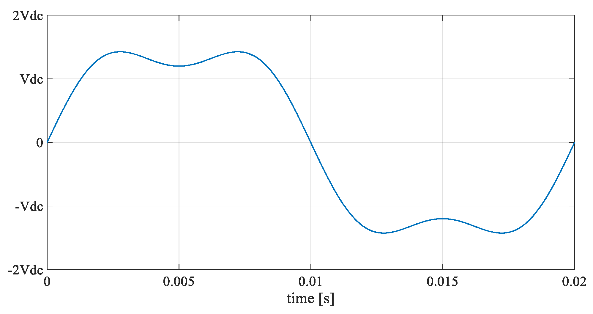
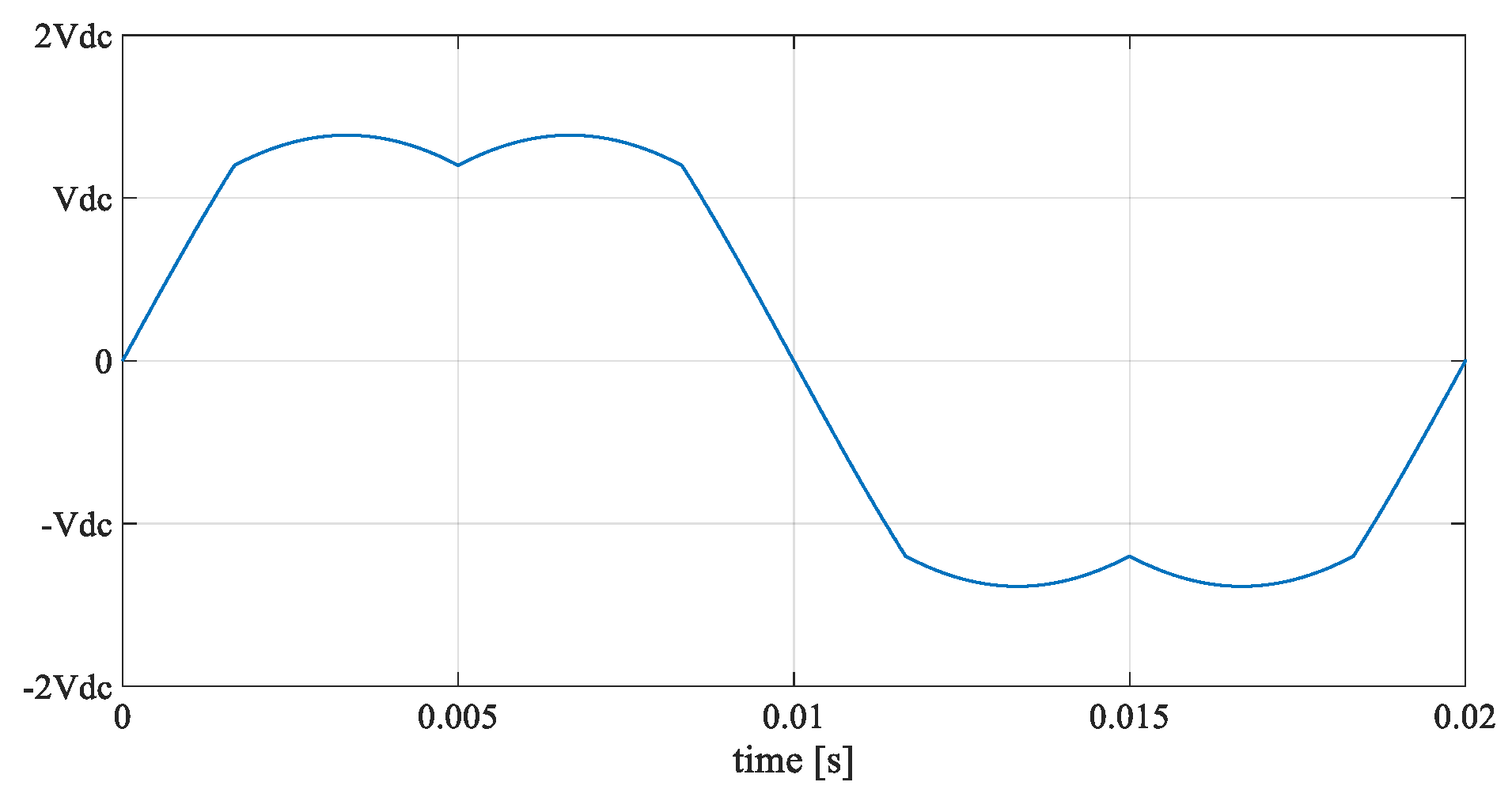
Depending on the modulating signal waveform, the following techniques can be obtained:

4. FPGA Design of the Control Software

The FPGA is commonly used in order to implement complex functions, such as Arithmetic Logic Unit (ALU), memories, communication units and so on [2]. It can be stated that this digital device, due to both its flexibility and high number of configurable digital outputs, is suitable for the implementation of the modulation techniques by using the traditional formula for the evaluation of the duty cycle, providing also higher accuracy in terms of design of the related algorithm, due to the possibility of choice of the frequencies for the clock signals. This section describes the main technical aspects related to the design, implementation and simulation of the control software.

4.1. Features of the Control Software

In order to design a digital system capable of generating the carrier and modulating signals and compare them in an adequate manner, the operations must be synchronized with respect to the chosen operating frequency.
The converter has been controlled with a modulating frequency equal to 10 kHz. The number of samples of the modulating signal is chosen based on the type of modulation. With the purpose of obtaining a synchronous modulation, the number of samples ns, which are required in the construction of the 50 Hz modulating signal, is given by:
n s = f P W M 50 .
From Equation (6), the number of obtained samples for the modulating wave is equal to 200. The updating of the modulating samples is managed with a CLKreference clock signal with a frequency equal to fPWM.
The number of samples of the carrier waves Ncarrier has been chosen equal to 1000 in order to obtain a good resolution. Based on this value, the frequency of the clock signal for the updating of the carrier samples can be determined as follows:
C L K c a r r i e r = f P W M · N c a r r i e r
Thus, the frequency of the CLKcarrier clock signal obtained from Equation (7) is equal to 10 MHz.

4.2. Digital System Design

The implemented digital system has been designed with the aim of obtaining a synchronous sequential system, so that the data flow can be managed from adequately synchronized timing signals, namely CLKreference and CLKcarrier, allowing the updating of the modulating and carrier signals, respectively. These signals are generated from the use of a digital Phase Locked Loop (PLL) circuit, whose input source is an external clock signal available in the control board, as reported in [41].
In order to increase the speed of computation of the entire digital system, the reference signals are generated from the use of a Look-Up Table (LUT) with dimensions and resolutions equal to 200 × 1 and 13 bit, respectively. The carrier signals are generated by adopting up-down binary counters with a resolution of 13 bit and the comparison between reference and carrier signals is realized by a 13-bit digital comparator. This circuit adopts the CLKreference as temporizing signal. Therefore, the comparison is achieved 1000 times for each PWM period equal to 100 μs. The output signals from the comparators represent the command signals for the upper components of the H-Bridges legs.
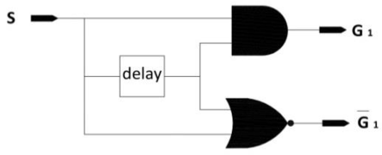
The generation of the command signals of the components of the lower H-Bridge legs, as well as the obtainment of the dead-time for the protection of the series-connected components, is achieved through the logic circuit shown in Figure 6. The delayed signal is obtained by using several cascaded-connected D flip-flops, whose number is dependent on the adopted clock signal. In order to obtain a 400 ns of delay, four D flip-flops have been connected and managed with the 10 MHz CLKcarrier clock signal.

4.3. FPGA and Software Environment

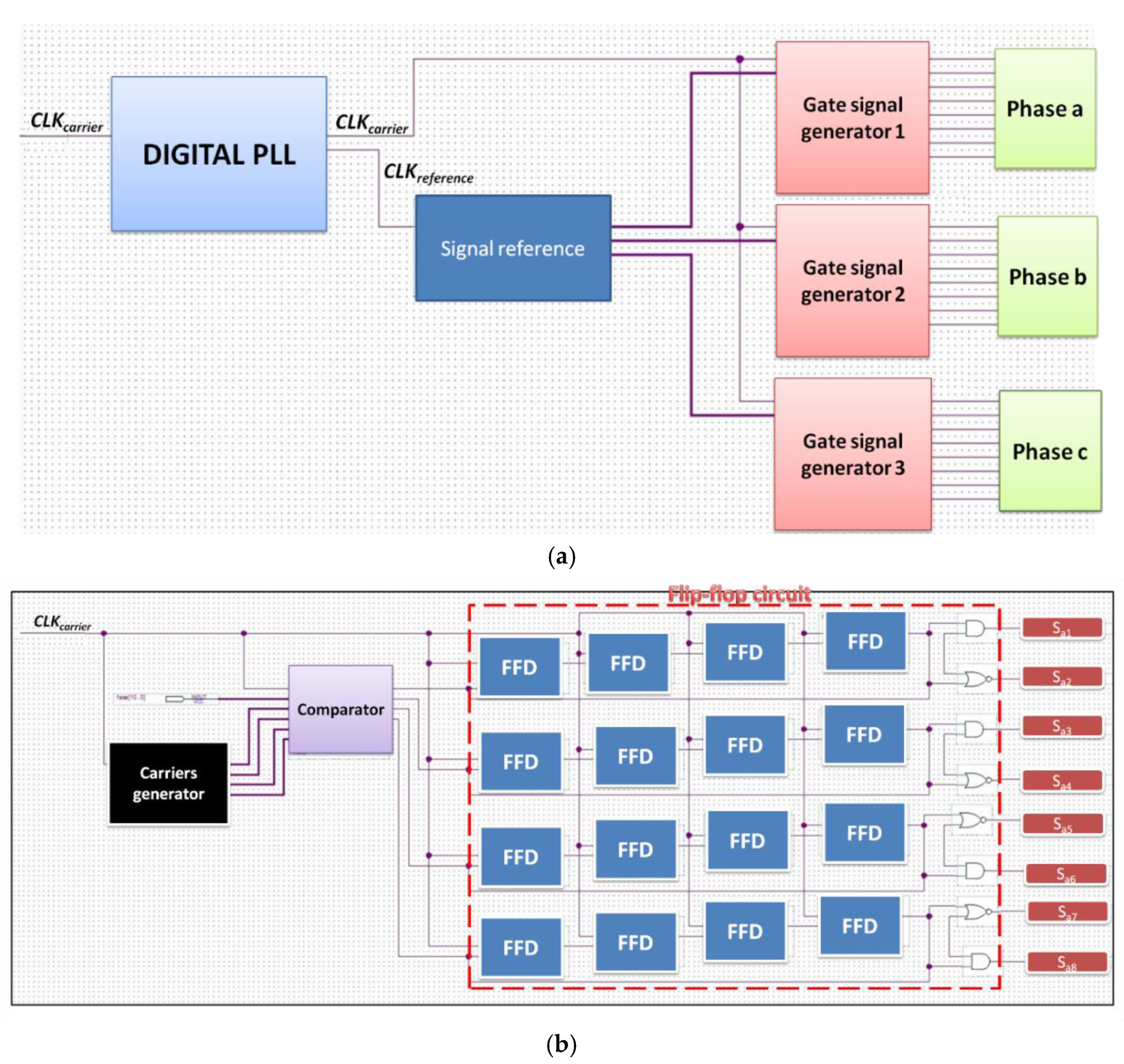
The digital signal above described has been implemented in a Cyclone III EP3C40Q FPGA (ALTERA®, San Jose, CA, USA). The software environment is Quartus II, produced by ALTERA®; VHDL has been adopted as programming language [42]. The block scheme of the implemented software is depicted in Figure 7a,b.
The digital PLL circuit (see Figure 7a) generates two synchronized clock signals, namely CLKreference and CLKcarrier, from an external clock signal. For each rising edge of the CLKreference clock, the signal generator block produces the modulating signals for each phase of the converter.
Inside the Gate signal generator block (see Figure 7b), the samples of triangular waves are available for each rising edge of the CLKcarrier clock signal. The carrier and modulating samples are compared during the falling edge. For each phase, the command signals are generated at the same instant of time, since the comparisons are realized in parallel.

4.4. Gate Level Simulation

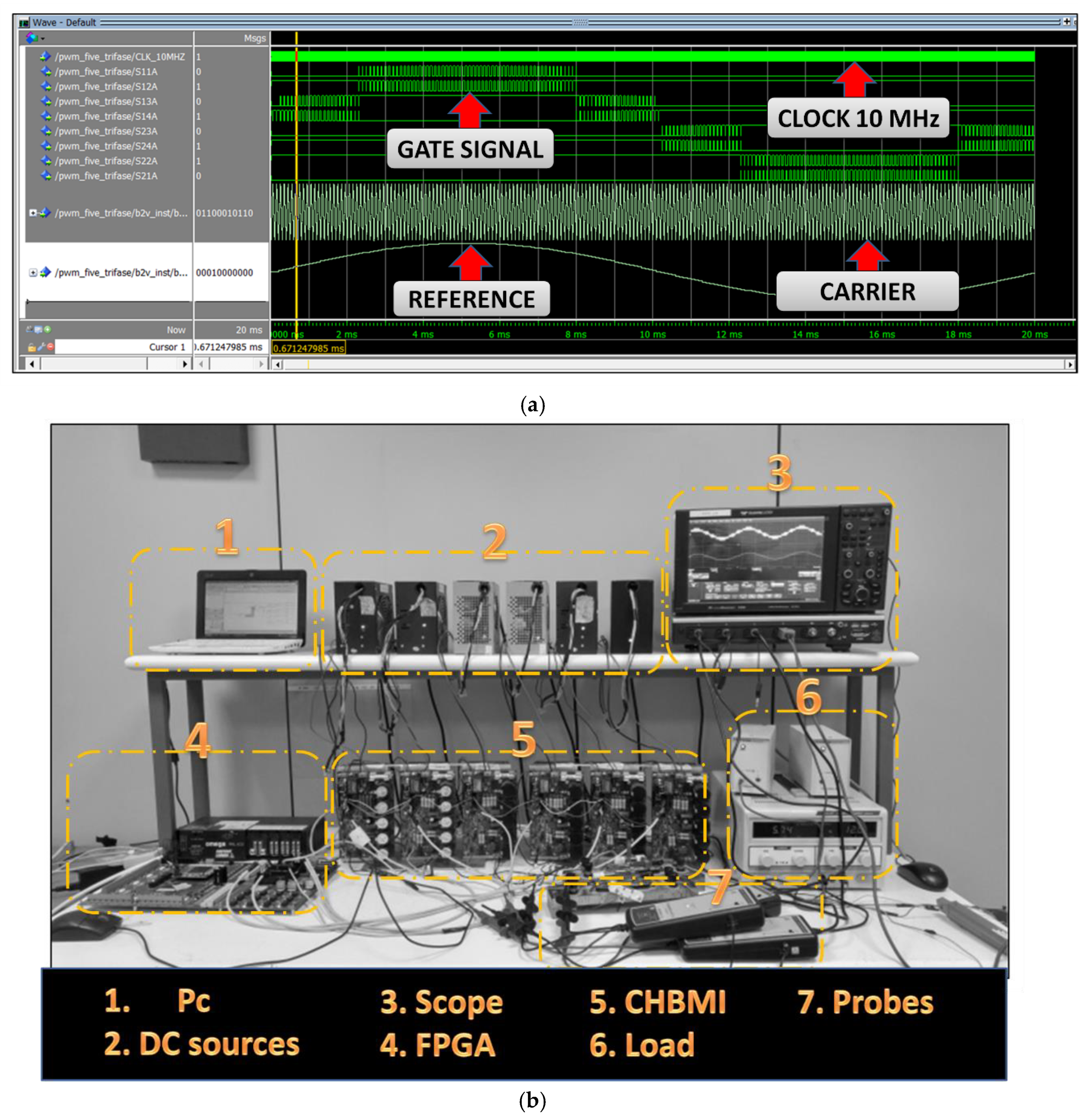
The correct working operation of the implemented control software has been simulated by means of the ModelSim environment produced by ALTERA®. Figure 8a shows the results of the simulation, which include the command signals of the components of one phase, the carrier signals and the sinusoidal modulating waveform. A photograph of the test bench is depicted in Figure 8b.

5. Comparison between Simulation and Experimental Results

In order to determine the harmonic content of the voltage waveforms produced by a CHBMI controlled by FPGA, the sinusoidal modulation techniques briefly reported in Section 3 have been taken into account due to their greater use in the field of industry applications. Moreover, as previously reported, this analysis is performed by considering the THD%, which can be evaluated as follows [39]:
T H D % = V r m s 2 V r m s , 1 2 V r m s , 1 2 · 100
where Vrms is the root mean square value of the phase voltage and Vrms,1 is the root mean square value of its fundamental harmonic.
For this purpose, in a first phase (simulation phase), the trends of both the phase and line-to-line voltages have been simulated by means of the Matlab/Simulink environment, in which the model of a 5-level CHBMI was implemented. Several simulations have been carried out with different values of the modulation index, ranging from 0.4 to 1.2.
In a second phase (experimental verification), the prototype of a 5-level CHBMI has been assembled and the related test bench (see Figure 8b), is mainly composed by:
  • A prototype of FPGA-based control board (Cyclone III–ALTERA®, DigiPowers.r.l);
  • Six power MOSFET-based H-bridge prototypes (model IRFB4115PbF, DigiPowers.r.l, city, country), whose technical features are summarized in Table 1;
  • A LeCroy WaveRunner 6Zi scope (Teledyne, city, state abbrev if USA, country) used for the real-time monitoring and acquisition of the related waveforms;
  • Six DC sources with 12 V of rated voltage;
  • A balanced RL three-phase electric load.
The voltage waveforms have been acquired by the Teledyne LeCroy WaveRunner 6Zi acquisition system with a number of samples equal to 1 Ms and in a time interval equal to 20 ms, corresponding to a sampling frequency of 50 MHz. The THD% values of the acquired waveforms have been, then, processed through means of the Matlab software.
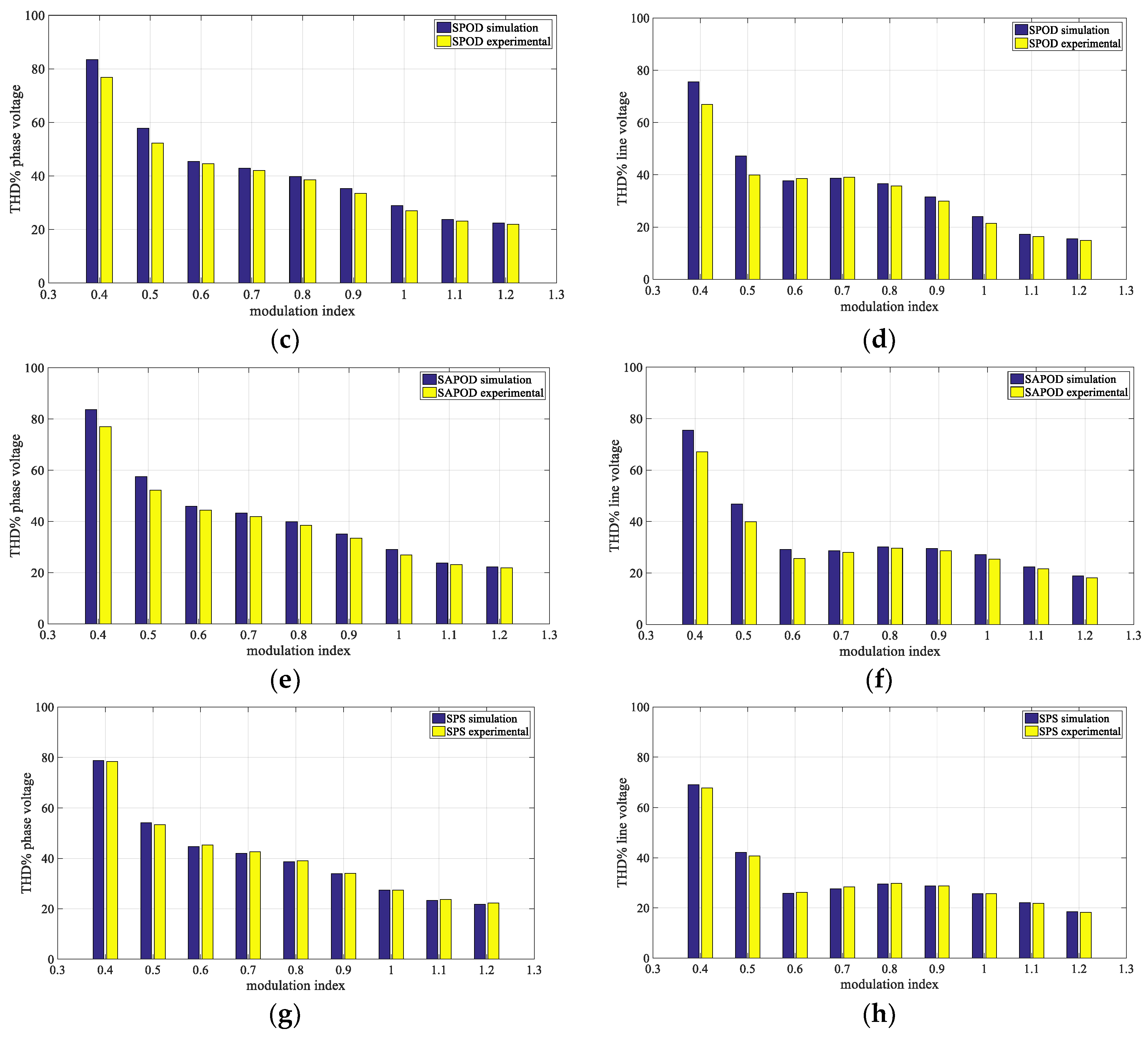
Figure 9 shows the comparison between the simulation and experimental values of THD% as function of m of both the phase and line voltage for each of the modulation techniques taken into account.
From Figure 10 it can be noticed that the THD% values experimentally obtained are comparable with those derived through simulations. This is due to both the implementation of parallel computing and the relatively high speed of processing of the FPGA.
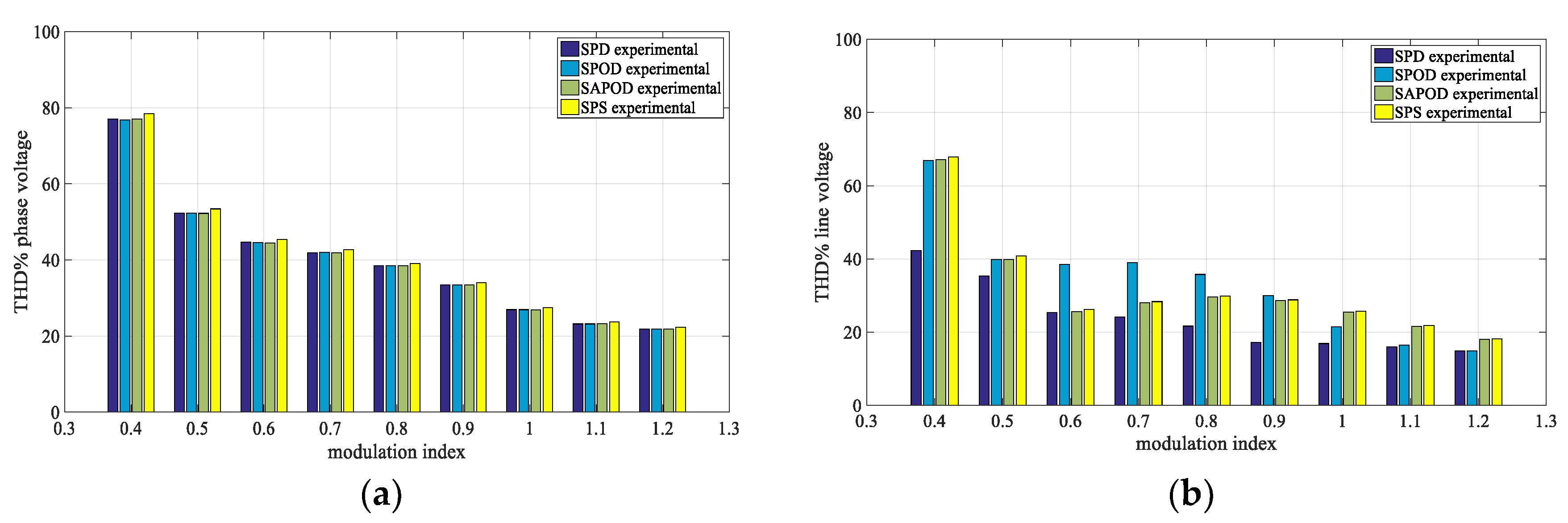
By referring to Figure 11, in which the experimental results are plotted all together for the phase voltage (Figure 11) and the line-to-line voltage (Figure 11), it is interesting to observe that the THD% values of the phase voltages for each modulation technique are almost close to each other. On the contrary, the THD% values for the line voltages significantly differ between the modulation techniques, with the lowest values corresponding to the SPD technique for any value of m. Moreover, the SAPOD technique presents the highest THD% values in the modulation range between 0.6 and 0.9.
The spectra of the SPD, SPOD and SAPOD modulation techniques present harmonics centered at a frequency fh equal to:
f h = k · f P W M
where fPWM is the switching frequency and k is an integer number.
On the contrary, by considering the harmonic spectrum of the SPS technique, the harmonics are centered at a frequency fh corresponding to:
f h = 4 k · f P W M
In order to deeply investigate the performance of the converter controlled by the previously described techniques, the harmonic spectra of the measured line voltages have been analyzed for two specific values of m, equal to 0.5 and 0.9. The first value corresponds to the condition of comparable THD% between the proposed modulation techniques, whereas the second value corresponds to the condition of minimum values of THD% within the linear region.
Table 2 summarizes the values obtained from this analysis and the corresponding trends of the line voltages for the eight conditions of Table 2 are all plotted in Figure 11 (m = 0.5) and Figure 12 (m = 0.9).
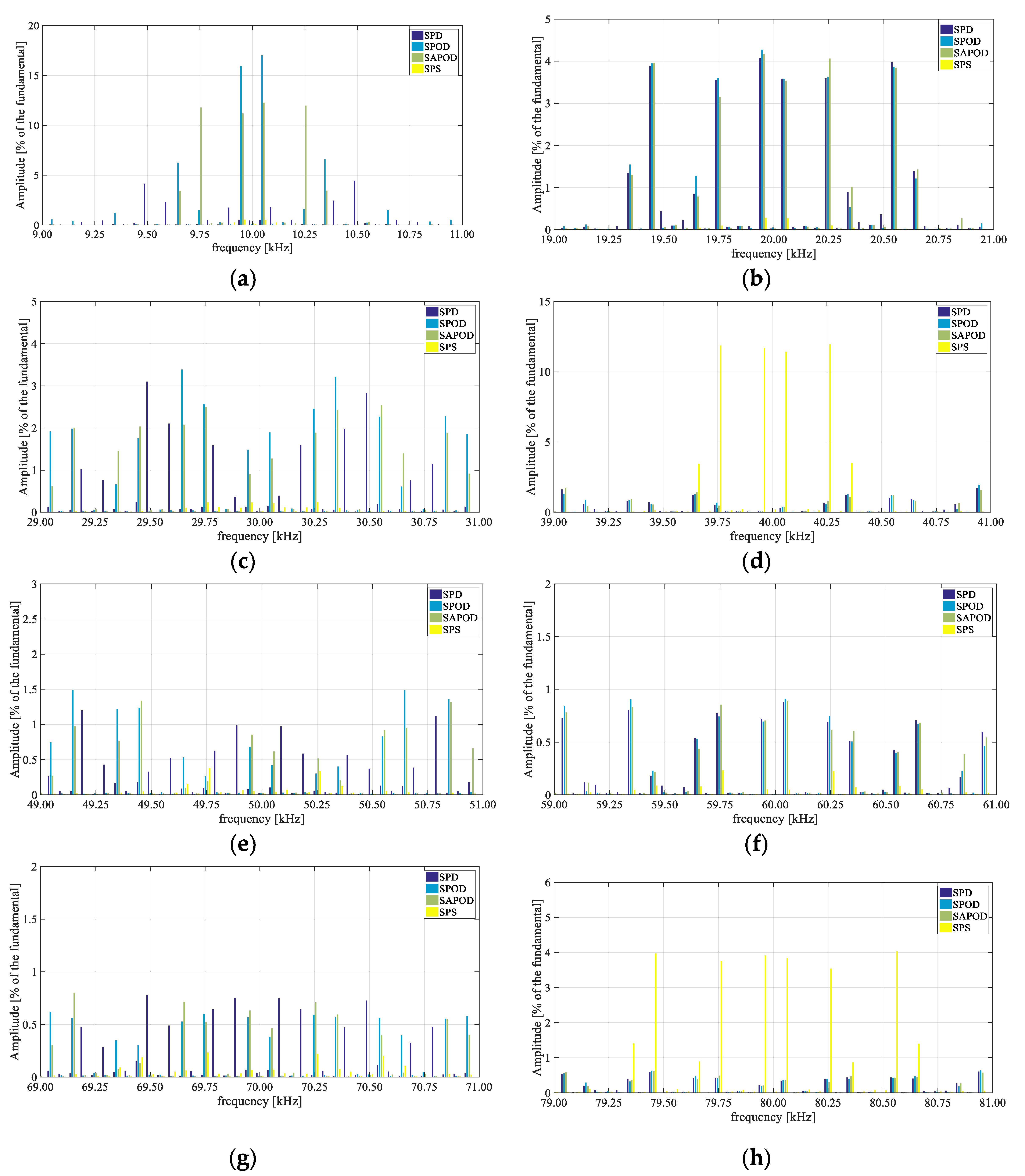
It can be noticed that these trends present differences in terms of voltage waveforms, at the same value of m. Figure 13 shows the comparison between the harmonic spectra centered around the switching frequency of 10 kHz (see Figure 14a) and their multiples from 20 kHz to 80 kHz (see Figure 14b–h) in the case of study of m=0.5 (the harmonic amplitudes are expressed as percentage of the fundamental harmonic).
For each frequency, only lateral bands are detected. Moreover, at the 10 kHz frequency and for odd values of k, the major contribution in terms of amplitude is given by the SPOD and SAPOD techniques, whereas the SPD presents a lower contribution, even with the presence of a higher number of harmonics.
Instead, for even values of k, the SPD, SPOD and SAPOD techniques present the same harmonic contribution both in terms of amplitude and spectra distribution. Moreover, the SPS technique presents harmonic content only for 2k multiples. The case of study of m = 0.9 is investigated in Figure 14, which shows the comparison between the harmonic spectra of the proposed techniques centered around the switching frequency of 10 kHz (see Figure 14a) and their multiples from 20 kHz to 80 kHz (see Figure 14b–h).
As in the previous case, only lateral bands are detected. In addition, in case of even values of k, the SPD, SPOD and SAPOD techniques present almost the same harmonic content and the SPS harmonics appear for frequencies equal to 4k. For odd values of k, the major harmonic contributions are given by the SPOD and SAPOD techniques, while the SPD presents the lowest contribution, except for the frequency equal to 70 kHz, in which the harmonic content is comparable in terms of amplitude. Therefore, from this analysis it can be stated that the different values of THD% depend on the harmonic components with frequencies corresponding to odd values of k.
The well-known equation for the determination of the THD is given by:
T H D = h = 2 V h 2 V 1
In order to evaluate the contribution produced by each modulation technique for each of the considered frequency fh, the following Approximate Total Harmonic Distortion formula, namely ATHD, is considered:
A T H D 2 = h = 9 11 V h 2 V 1 2 + h = 19 21 V h 2 V 1 2 + h = ( k f P W M 1 ) ( k f P W M + 1 ) V h 2 V 1 2
The ATHD is based on distributing Equation (11) only for the frequencies of interest, as shown by Equation (12). Thus, the sum is extended only within the range of the analyzed frequencies and, therefore, each sum defines a partial THD (PTHD). Consequentially, the ATHD can be also expressed as function of the PTHD:
A T H D 2 = P T H D 10 k H z + P T H D 20 k H z + + P T H D k f P W M
A T H D = h = f P W M k f P W M P T H D h
Furthermore, the PTHD values allow the evaluation of the contribution to the ATHD for each modulation technique.
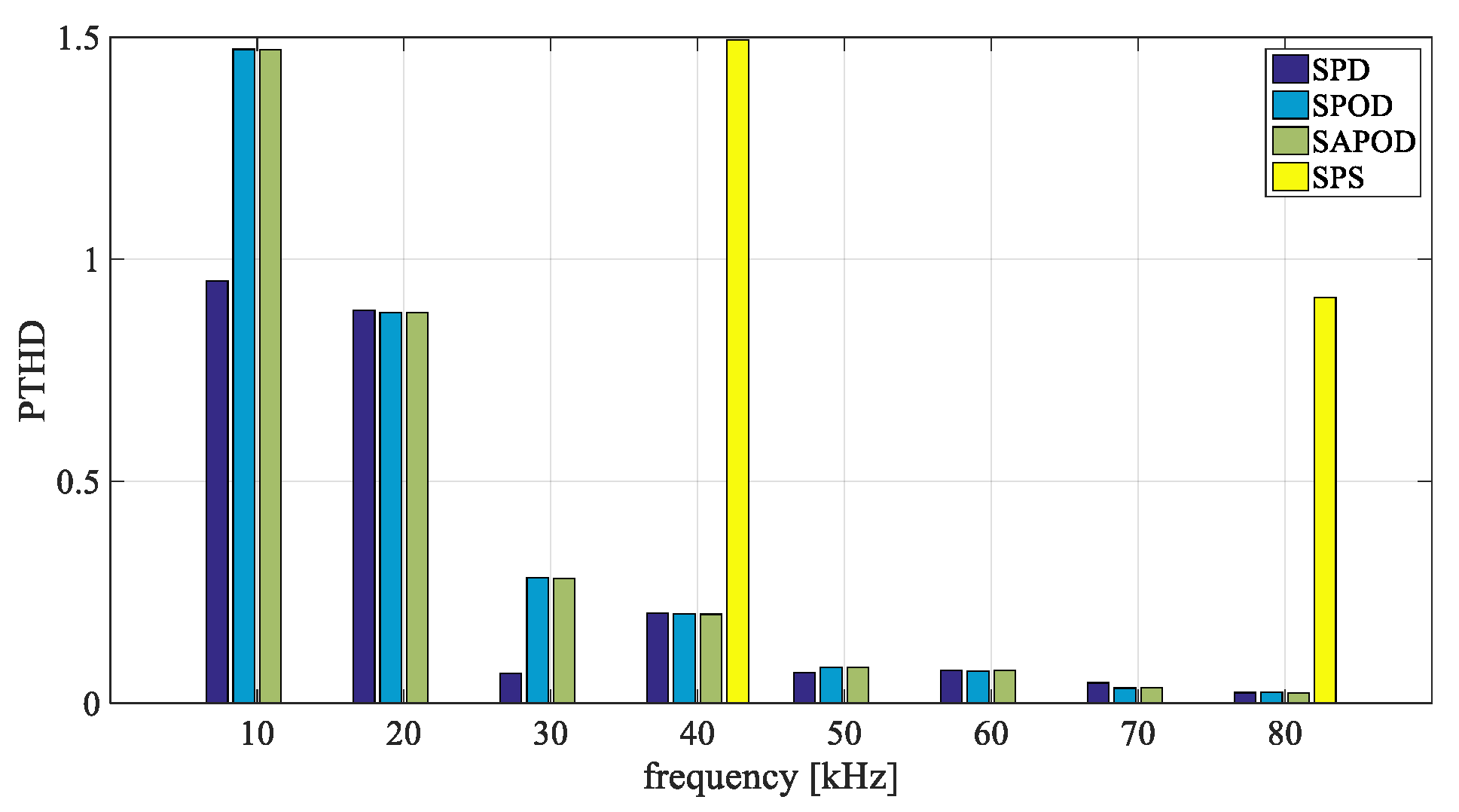
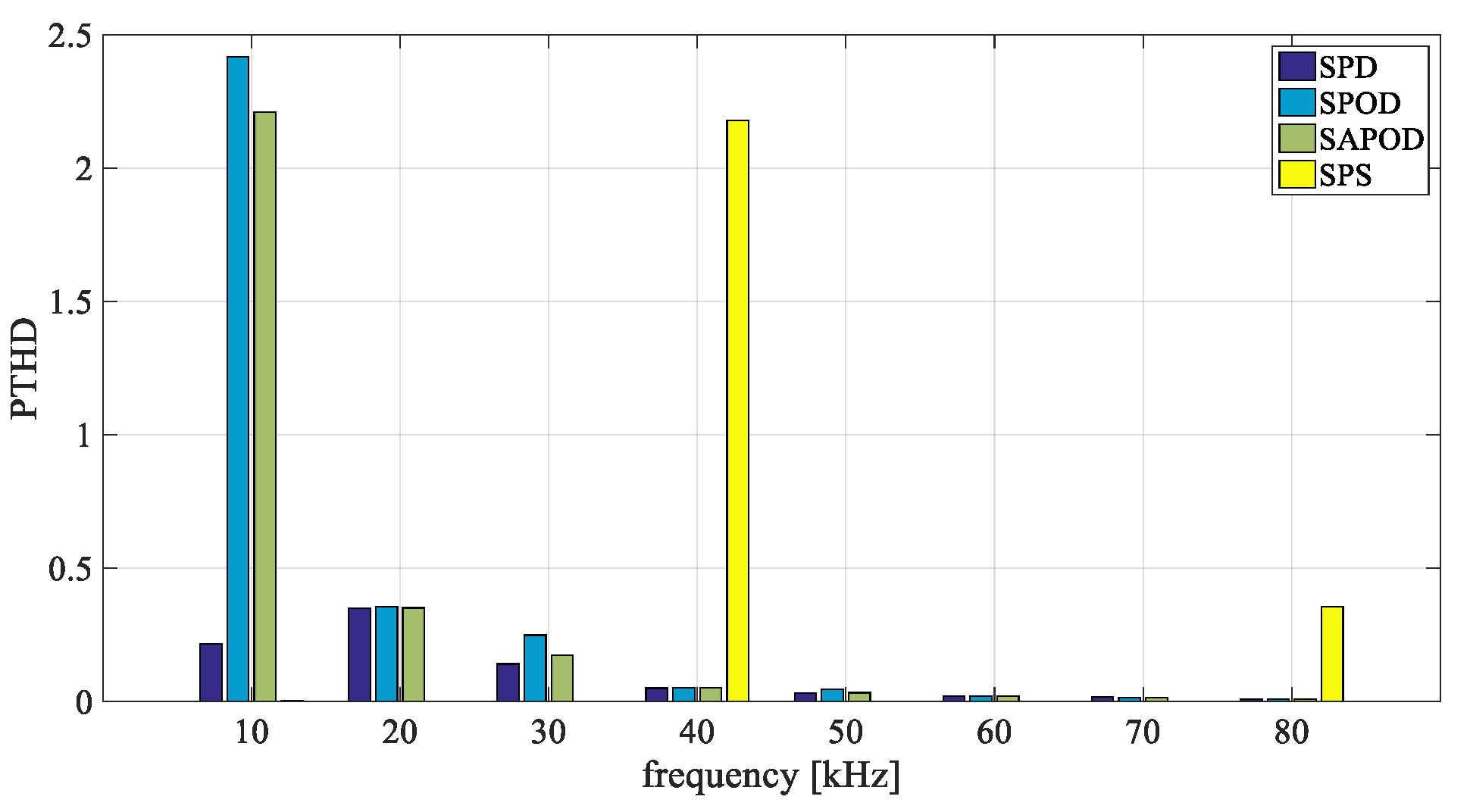
Figure 15 and Figure 16 show the PTHD values computed for the two cases. From this graphical view, it can be noticed that the SPD technique provides the lowest harmonic contribution (the highest difference can be detected for f = 10 kHz and m = 0.5), whereas the SPS technique gives the major contribution at the frequencies of 40 kHz and 80 kHz.

6. Conclusions

This paper has presented the performance of a CHBMI five-level three phase with an FGPA-based controller. The first step of this analysis has provided a comparison between the simulation and experimental results obtained from the multicarrier modulation techniques with sinusoidal waveform as reference signal. Both for the phase and line voltages, the THD% values computed from the simulations and from the experimental data are almost comparable to each other, for any of the considered modulation techniques and independently from the value of the modulation index, demonstrating the high-performance of the FPGA control system.
Even though the obtained THD% values for the phase voltage are comparable between the proposed modulation techniques independently from the value of modulation index, the THD% related to the line-to-line voltage differ among the techniques, with the lowest contribution provided by the SPD technique.
Finally, the line voltage harmonic spectra for two specific cases of study (m = 0.5 and m = 0.9) have been taken into account by evaluating the THD% in the frequency range of interest for each of the proposed described modulation technique. From this comparison, it can be stated that the SPD technique provides the lowest contribution for each of the considered frequency range.

Author Contributions

Conceptualization, G.S., F.V. and M.C.; methodology, R.M.; software, F.P.; validation, G.S.; writing—review and editing, G.S., F.V. and M.C.; supervision, G.A. and M.T.

Funding

This research received no external funding. This work was financially supported by MIUR–Ministero dell’Istruzione dell’Università e della Ricerca (Italian Ministry of Education, University and Research) and by SDESLab (Sustainable Development and Energy Saving Laboratory) and LEAP (Laboratory of Electrical APplications) of the University of Palermo.

Conflicts of Interest

The authors declare no conflict of interest.

References

  1. Buccella, C.; Cecati, C.; Latafat, H. Digital Control of Power Converters—A Survey. IEEE Trans. Ind. Inform. 2012, 8, 437–447. [Google Scholar] [CrossRef]
  2. Monmasson, E.; Cirstea, M.N. FPGA Design Methodology for Industrial Control Systems—A Review. IEEE Trans. Ind. Electron. 2007, 54, 1824–1842. [Google Scholar] [CrossRef]
  3. Monmasson, E.; Idkhajine, L.; Cirstea, M.N.; Bahri, I.; Tisan, A.; Naouar, M.W. FPGAs in Industrial Control Applications. IEEE Trans. Ind. Inform. 2011, 7, 224–243. [Google Scholar] [CrossRef] [Green Version]
  4. Rodríguez-Andina, J.J.; Valdés-Peña, M.D.; Moure, M.J. Advanced Features and Industrial Applications of FPGAs—A Review. IEEE Trans. Ind. Inform. 2015, 11, 853–864. [Google Scholar] [CrossRef]
  5. Sulaiman, N.; Obaid, Z.A.; Marhaban, M.H.; Hamidon, M.N. Design and implementation of FPGA-based systems—A review. Aust. J. Basic Appl. Sci. 2009, 3, 3575–3596. [Google Scholar]
  6. Kung, Y.; Fung, R.; Tai, T. Realization of a Motion Control IC for X-Y Table Based on Novel FPGA Technology. IEEE Trans. Ind. Electron. 2009, 56, 43–53. [Google Scholar] [CrossRef]
  7. Patel, J.; Sood, V.K. Review of Digital Controllers in Power Converters. In Proceedings of the 2018 IEEE Electrical Power and Energy Conference (EPEC), Toronto, ON, Canada, 10–11 October 2018; pp. 1–8. [Google Scholar] [CrossRef]
  8. Islam, M.R.; Guo, Y.; Zhu, J. FPGA-based control of modular multilevel converters: Modeling and experimental evaluation. In Proceedings of the 2015 International Conference on Electrical & Electronic Engineering (ICEEE), Rajshahi, Bangladesh, 4–6 November 2015; pp. 89–92. [Google Scholar] [CrossRef]
  9. Zhou, Z.; Wang, Q.; Lin, R. Real-time Simulation Realization of Modular Multilevel Converter Based on FPGA. In Proceedings of the 2018 IEEE International Power Electronics and Application Conference and Exposition (PEAC), Shenzhen, China, 4–7 November 2018; pp. 1–6. [Google Scholar]
  10. Atoui, E.B.; Mesbah, T.; Atoui, H. FPGA Implementation of Multi-carriers PWM Technique for Modular Multi-level Inverter. In Proceedings of the 2018 International Conference on Applied Smart Systems (ICASS), Medea, Algeria, 24–25 November 2018; pp. 1–6. [Google Scholar]
  11. Reddy, B.P.; Keerthipati, S. Torque Ripple Minimization of PPMIM Drives with Phase-Shifted Carrier PWM. In Proceedings of the IECON 2018—44th Annual Conference of the IEEE Industrial Electronics Society, Washington, DC, USA, 21–23 October 2018; pp. 725–730. [Google Scholar]
  12. Sumam, M.J.; Shiny, G. Rapid Prototyping of High Performance FPGA Controller for an Induction Motor Drive. In Proceedings of the 2018 8th International Conference on Power and Energy Systems (ICPES), Colombo, Sri Lanka, 21–22 December 2018; pp. 76–80. [Google Scholar]
  13. Aime, M.; Gateau, G.; Meynard, T. Implementation of a peak current control algorithm within a field programmable gate array. IEEE Trans. Ind. Electron. 2007, 54, 406–418. [Google Scholar] [CrossRef]
  14. Gateau, G.; Lienhardt, A.M.; Meynard, T. Digital sliding mode observer implementation using FPGA. IEEE Trans. Ind. Electron. 2007, 54, 1865–1875. [Google Scholar]
  15. Coppola, M.; Napoli, F.D.; Guerriero, P.; Iannuzzi, D.; Daliento, S.; Pizzo, A.D. An FPGA-based advanced control strategy of a grid-tied PV CHB inverter. IEEE Trans. Power Electron. 2016, 31, 806–816. [Google Scholar] [CrossRef]
  16. Moranchel, M.; Huerta, F.; Sanz, I.; Bueno, E.; Rodríguez, F.J. A Comparison of Modulation Techniques for Modular Multilevel Converters. Energies 2016, 9, 1091. [Google Scholar] [CrossRef]
  17. Prabaharan, N.; Arun, V.; Sanjeevikumar, P.; Mihet-Popa, L.; Blaabjerg, F. Reconfiguration of a Multilevel Inverter with Trapezoidal Pulse Width Modulation. Energies 2018, 11, 2148. [Google Scholar] [CrossRef]
  18. Jayaraman, M.; Vt, S. Power Quality Improvement in a Cascaded Multilevel Inverter Interfaced Grid Connected System Using a Modified Inductive–Capacitive–Inductive Filter with Reduced Power Loss and Improved Harmonic Attenuation. Energies 2017, 10, 1834. [Google Scholar] [CrossRef]
  19. Xue, F.; Ling, Z.; Yang, Y.; Miao, X. Design and Implementation of Novel Smart Battery Management System for FPGA Based Portable Electronic Devices. Energies 2017, 10, 264. [Google Scholar] [CrossRef]
  20. Ricco, M.; Mathe, L.; Monmasson, E.; Teodorescu, R. FPGA-Based Implementation of MMC Control Based on Sorting Networks. Energies 2018, 11, 2394. [Google Scholar] [CrossRef]
  21. Rodič, M.; Milanovič, M.; Truntič, M. Digital Control of an Interleaving Operated Buck-Boost Synchronous Converter Used in a Low-Cost Testing System for an Automotive Powertrain. Energies 2018, 11, 2290. [Google Scholar] [CrossRef]
  22. Zhang, B.; Wang, Y.; Tu, S.; Jin, Z. FPGA-Based Real-Time Digital Solver for Electro-Mechanical Transient Simulation. Energies 2018, 11, 2650. [Google Scholar] [CrossRef]
  23. Naouar, M.W.; Monmasson, E.; Naassani, A.A.; Slama-Belkhodja, I.; Patin, N. FPGA-Based Current Controllers for AC Machine Drives—A Review. IEEE Trans. Ind. Electron. 2007, 54, 1907–1925. [Google Scholar] [CrossRef]
  24. Rodriguez, J.; Lai, J.-S.; Peng, F.Z. Multilevel inverters: A survey of topologies, controls, and applications. IEEE Trans. Ind. Electron. 2002, 49, 724–738. [Google Scholar] [CrossRef]
  25. De, S.; Banerjee, D.; Kumar, K.S.; Gopakumar, K.; Ramchand, R.; Patel, C. Multilevel inverters for low-power application. IET Power Electron. 2011, 4, 384–392. [Google Scholar] [CrossRef]
  26. Beig, A.R.; Dekka, A. Experimental verification of multilevel inverter-based standalone power supply for low-voltage and low-power applications. IET Power Electron. 2012, 5, 635–643. [Google Scholar] [CrossRef]
  27. Behrouzian, E.; Bongiorno, M.; de la Parra, H.Z. An overview of multilevel topologies for grid connected applications. In Proceedings of the 2013 15th European Conference on Power Electronics Applications (EPE), Lille, France, 2–6 September 2013. [Google Scholar]
  28. Rashid, M.H. Power Electronics Handbook, Devices, Circuits and Applications, 3rd ed.; Buttherworth-Heirnann: Oxford, UK, 2011. [Google Scholar]
  29. Gupta, K.K.; Jain, S. Topology for multilevel inverters to attain maximum number of levels from given DC sources. IET Power Electron. 2012, 5, 435–446. [Google Scholar] [CrossRef]
  30. Jamaludin, J.; Rahim, N.A.; Ping, H.W. Multilevel voltage source inverter with optimised usage of bidirectional switches. IET Power Electron. 2015, 8, 378–390. [Google Scholar] [CrossRef] [Green Version]
  31. Gautam, S.P.; Kumar, L.; Gupta, S. Hybrid topology of symmetrical multilevel inverter using less number of devices. IET Power Electron. 2015, 8, 2125–2135. [Google Scholar] [CrossRef]
  32. ShalchiAlishah, R.; Nazarpour, D.; Hosseini, S.H.; Sabahi, M. Novel multilevel inverter topologies for medium and high-voltage applications with lower values of blocked voltage by switches. IET Power Electron. 2014, 7, 3062–3071. [Google Scholar] [CrossRef]
  33. Adam, G.P.; Anaya-Lara, O.; Burt, G.M.; Telford, D.; Williams, B.W.; Mcdonald, J.R. Modular multilevel inverter: Pulse width modulation and capacitor balancing technique. IET Power Electron. 2010, 3, 702–715. [Google Scholar] [CrossRef]
  34. Haji-Esmaeili, M.M.; Naseri, M.; Khoun-Jahan, H.; Abapour, M. Fault-tolerant structure for cascaded H-bridge multilevel inverter and reliability evaluation. IET Power Electron. 2017, 10, 59–70. [Google Scholar] [CrossRef]
  35. McGrath, B.P.; Holmes, D.G. Multicarrier PWM strategies for multilevel inverters. IEEE Trans. Ind. Electron. 2002, 49, 858–867. [Google Scholar] [CrossRef]
  36. Balamurugan, C.R.; Natarajan, S.P.; Bensraj, R.; Shanthi, B. A Review on Modulation Strategies of Mulilevel Inverter. Indones. J. Electr. Eng. Comput. Sci. 2016, 3, 681–705. [Google Scholar] [CrossRef]
  37. Schettino, G.; Buccella, C.; Caruso, M.; Cecati, C.; Castiglia, V.; Miceli, R.; Viola, F. Overview and experimental analysis of MC SPWM techniques for single-phase five level cascaded H-bridge FPGA controller-based. In Proceedings of the IECON 2016—42nd Annual Conference of the IEEE Industrial Electronics Society, Florence, Italy, 23–26 October 2016; pp. 4529–4534. [Google Scholar] [CrossRef]
  38. Benanti, S.; Buccella, C.; Caruso, M.; Castiglia, V.; Cecati, C.; di Tommaso, A.O.; Miceli, R.; Romano, P.; Schettino, G.; Viola, F. Experimental analysis with FPGA controller-based of MC PWM techniques for three-phase five level cascaded H-bridge for PV applications. In Proceedings of the 2016 IEEE International Conference on Renewable Energy Research and Applications (ICRERA), Birmingham, UK, 20–23 November 2016; pp. 1173–1178. [Google Scholar] [CrossRef]
  39. Miceli, R.; Schettino, G.; Viola, F. A novel computational approach for harmonic mitigation in PV systems with single-phase five-level CHBMI. Energies 2018, 11, 2100. [Google Scholar] [CrossRef]
  40. Viola, F. Experimental evaluation of the performance of a three-phase five-level cascaded h-bridge inverter by means FPGA-based control board for grid connected applications. Energies 2018, 11, 3298. [Google Scholar] [CrossRef]
  41. Dordevic, O.; Jones, M.; Levi, E. Analytical Formulas for Phase Voltage RMS Squared and THD in PWM Multiphase Systems. IEEE Trans. Power Electron. 2015, 30, 1645–1656. [Google Scholar] [CrossRef] [Green Version]
  42. ALTERA, Cyclone III Device Handbook—Volume 1, 101 Innovation Drive San Jose, CA 95134. Available online: http://www.altera.com (accessed on 14 March 2019).
  43. International Rectifier. Data Sheet IRFB4115PbF. 2014. Available online: www.irf.com (accessed on 14 March 2019).
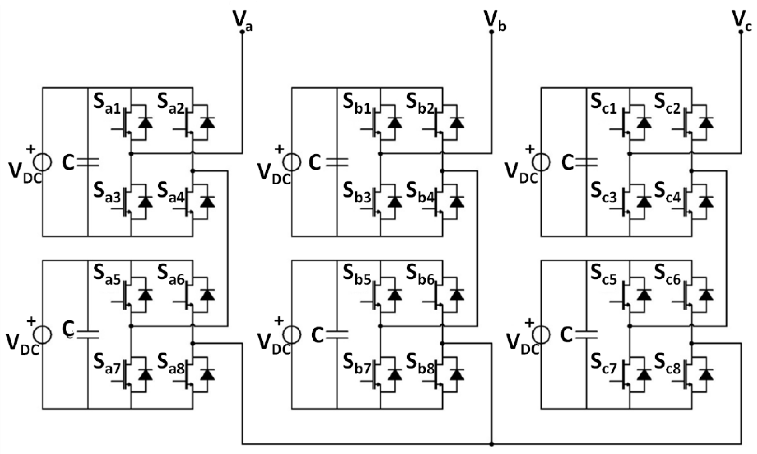
Figure 1. Three-phase, five-level structure of a CHBMI.
Energies 12 01016 g001
Figure 2. Multicarrier modulation techniques for five-level inverter. (a) Sinusoidal Phase Disposition (SPD). (b) Sinusoidal Phase Opposition Disposition (SPOD). (c) Sinusoidal Alternative Phase Opposition Disposition (APOD). (d) Sinusoidal Phase-Shifted (SPS).
Energies 12 01016 g002aEnergies 12 01016 g002b
Figure 3. Sinusoidal modulating signal.
Energies 12 01016 g003
Figure 4. Third Harmonic Injection (THI) modulating signal.
Energies 12 01016 g004
Figure 5. SFO (Switching Frequency Optimal) modulating signal.
Energies 12 01016 g005
Figure 6. Logic circuit for the dead-time generation.
Energies 12 01016 g006
Figure 7. Block scheme of the control software: (a) Main schematic, (b) Gate signal generator for one phase. PLL: Phase Locked Loop; FFD: Flip-Flop Device.
Energies 12 01016 g007
Figure 8. Experimental implementation: (a) Gate level simulation results and (b) a photograph of the test bench.
Energies 12 01016 g008
Figure 9. Comparison between the simulated (blue) and the experimental (yellow) THD% values. (a) Phase Voltage-SPD; (b) Line Voltage-SPD; (c) Phase Voltage-SPOD; (d) Line Voltage-SPOD; (e) Phase Voltage-SAPOD; (f) Line Voltage-SAPOD; (g) Phase Voltage-SPS; (h) Line Voltage-SPS.
Energies 12 01016 g009aEnergies 12 01016 g009b
Figure 10. Comparison between the experimental THD% results for (a) phase voltage and (b) line voltage.
Energies 12 01016 g010
Figure 11. Line voltage waveforms acquired with a modulation index equal to 0.5.
Energies 12 01016 g011
Figure 12. Line voltage waveforms acquired with a modulation index equal to 0.9.
Energies 12 01016 g012
Figure 13. Comparison between the harmonic spectra around the center of multiples of the switching frequency for m equal to 0.5: SPD (blue bar), SPOD (light-blue bar), SAPOD (green bar) and SPS (yellow bar). (a) harmonic spectrum centered at 10 kHz; (b) harmonic spectrum centered at 20 kHz; (c) harmonic spectrum centered at 30 kHz; (d) harmonic spectrum centered at 40 kHz; (e) harmonic spectrum centered at 50 kHz; (f) harmonic spectrum centered at 60 kHz; (g) harmonic spectrum centered at 70 kHz; (h) harmonic spectrum centered at 80 kHz.
Energies 12 01016 g013
Figure 14. Comparison between the harmonic spectra around the center of multiples of the switching frequency for m equal to 0.9: SPD (blue bar), SPOD (light-blue bar), SAPOD (green bar) and SPS (yellow bar). (a) harmonic spectrum centered at 10 kHz; (b) harmonic spectrum centered at 20 kHz; (c) harmonic spectrum centered at 30 kHz; (d) harmonic spectrum centered at 40 kHz; (e) harmonic spectrum centered at 50 kHz; (f) harmonic spectrum centered at 60 kHz; (g) harmonic spectrum centered at 70 kHz; (h) harmonic spectrum centered at 80 kHz.
Energies 12 01016 g014
Figure 15. Comparison of PTHD values for modulation index equal to 0.5.
Energies 12 01016 g015
Figure 16. Comparison of PTHD values for modulation index equal to 0.9.
Energies 12 01016 g016
Table 1. Features of the IRFB4115PBF device [43].
Magnitude (unit)SymbolValue
Voltage (V)Vdss150
Resistance (mΩ)Rds(on)9.3
Current (A)Id (siliconlimited)104
Turn on delay (ns)TD(ON)18
Rise time (ns)tR, rise time73
Turn off delay (ns)TD(OFF),41
Fall time (ns)tF39
Reversal recovery (ns)tRR86
Table 2. THD% for modulation indexes equal to 0.5 and 0.9.
Modulation TechniqueTHD% m = 0.5THD% m = 0.9
SPD35.38%17.19%
SPOD39.88%29.95%
SAPOD39.87%28.64%
SPS40.77%28.83%