Article

An MPC Reference Governor Approach for Enhancing the Performance of Precompensated Boost DC–DC Converters

Department of Automation Engineering, Alexander Technological Educational Institute (ATEI) of Thessaloniki, Sindos 57400, Greece
Energies 2019, 12(3), 563; https://doi.org/10.3390/en12030563
Submission received: 11 January 2019 / Revised: 8 February 2019 / Accepted: 10 February 2019 / Published: 12 February 2019

Abstract

:
This article addresses the problem of enhancing the performance of boost DC–DC converters that are already compensated either in voltage-mode by a common proportional–integral–derivative (PID, Type III) primary controller or in current-mode with a two-loop PI control law. Improved performance may be obtained with the addition of a secondary controller/prefilter in the form of a reference governor. This complementary scheme adjusts the imposed voltage reference input signal dynamically and can be designed in an optimal fashion via the model predictive control (MPC) methodology. Our evaluation with numerical simulation in MATLAB suggests that this two-level controller can effectively enhance the performance of a DC–DC boost converter in a wide operating range without imposing extra requirements or limitations. A simple linear MPC design in explicit form is employed in this approach, which is computationally tractable for digital microprocessor implementation. This work paves the way for future research involving reference governor ideas in the area of bilinear power electronic converters.

1. Introduction

Reference governor techniques have only very recently appeared in the power electronics field [1,2,3]. Such ideas have been developed theoretically for over two decades and already applied to other engineering fields, mainly in the automotive industry and robotics (see, e.g., [4,5,6] and references therein). Especially for the more demanding types of DC–DC converters (i.e., boost converters with nonlinear dynamics), many advanced control methods have been recently proposed with the aim of improving their transient response and robustness [7,8,9,10,11,12,13], including model predictive control (MPC) technology [14,15,16,17,18,19]. The vast majority of the control algorithms developed are replacements to the primal controller, resulting in an increased complexity and implementation cost. However, there are many cases in which the main controller is already hard-coded or implemented in low-cost hardware with certified performance, stability, and robustness, which we would not like to sacrifice or which is not possible to replace. Instead of replacing this controller, a new idea is to complement it with a secondary, higher-level controller that provides a dynamically modified reference signal to the primal controller. This idea results in a two-loop control structure, where the outer loop provides a modified reference to the inner loop and can also run in a different (slower) rate as it usually involves on-line (e.g., MPC) optimization.
In this paper, the idea of using an MPC reference governor scheme is applied for the first time, to the best of the author’s knowledge, to a voltage-mode-controlled boost DC–DC converter. A similar technique has been recently tested for a DC–DC buck converter controlled by a simple proportional–integral (PI) primary controller [1]. However, the case of a boost converter presents further nontrivial challenges as its dynamics are nonlinear (bilinear), it is a nonminimum phase system, and it requires a much more complicated primary controller. The so-called PI–derivative (PID) Type III controller is an industrial standard for boost converters [20,21]; however, further performance enhancement is possible using a predictive controller and a hybrid scheme combining PID and predictive controllers, as shown in [22]. Considering a standard PID Type III primary controller, this work demonstrates that an MPC reference governor in explicit form can be found that provides improved performance without imposing more stringent operational requirements (higher currents or component stress) or extra constraints. This framework can offer improvements and more degrees of freedom compared to the results of [22], at the expense of added complexity. These findings are supported by extensive simulation results.
Additionally, current-mode, two-loop PI controllers, which are quite common for boost converters, are also studied. Similar MPC reference governor ideas are applied and performance improvements are also obtained, especially in disturbance rejection tasks and soft-start startup situations.
This paper is structured as follows. Section 2 describes the DC–DC boost converter, and Section 3 outlines the basic controllers used in the literature. The main results are included in Section 4, Section 5 and Section 6. Section 4 provides a detailed exposition of the design procedure for the proposed voltage-mode MPC reference governor scheme, while Section 5 presents a thorough evaluation with numerical simulation results. The current-mode scheme is presented in Section 6. The final section concludes.

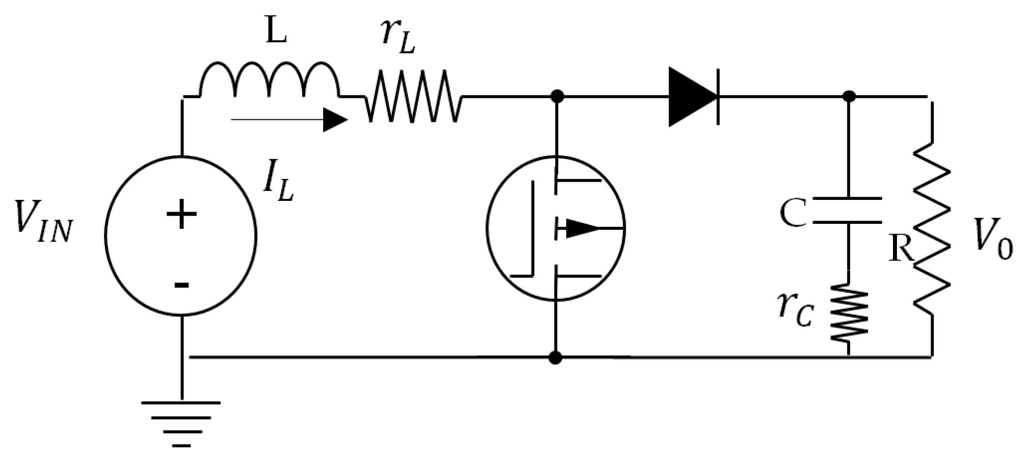
2. DC–DC Boost Converter

The circuit diagram of the boost converter considered in this paper is shown in Figure 1. A nonideal circuit with parasitic elements of the inductor and the capacitor was adopted. For comparison purposes, the values and the parameter ranges used were taken from [22], and they are summarized in Table 1, where f s is the switching frequency of the pulse width modulator (PWM), and D is the duty cycle taking values in the interval [0, 1].
A common averaging small-signal analysis (see, e.g., [23]) leads to a typical transfer function from the duty cycle d ( t ) to the output voltage v 0 ( t ) in the following form:
G v 0 d ( s ) = v 0 ( s ) d ( s ) = G d 0 ( 1 + s ω Z 1 ) ( 1 s ω R H P Z ) 1 + s ω 0 Q + s 2 ω 0 2
with one zero ω Z C in the left half plane, another zero ω R H P Z in the right half plane (nonminimum phase behavior), and two poles parameterized by the frequency ω 0 and the quality factor Q , where
G d 0 = V I N ( D ) 2 = V 0 2 V I N ,   ω 0 = 1 L C r L + R   ( D ) 2 R 1 L C V I N V 0 ,   D   = 1 D , ω Z 1 = 1 C   r C ,   ω R H P Z R L ( V I N V 0 ) 2 , Q = ω 0 r L L + 1 C ( R +   r C )

3. PID Type III and ARMarkov Predictive Control Design

A standard control strategy in industrial applications, including power electronics, is the PID controller. A special form of practical PID with three poles and two zeros, a double pole (second-order filter for high-frequency roll-off and noise mitigation), and a double zero (offering the necessary phase boost) is typically used in power electronics. It is known as the Type III compensator (see Figure 2), and its design is usually performed based on the so-called small-signal model of the converter in the frequency domain [23]. Typical requirements are a phase margin (PM) above 45° and a gain margin (GM) over 10 dB. In the present work, and as a reference point for assessing the performance of the proposed MPC reference governor scheme, the design presented in [22] was adopted. The transfer function of the Type III compensator is as follows:
G P I D ( s ) = k P I D s ( 1 + s ω Z C ) 2 ( 1 + s ω P C ) 2 , ω P C = 10   a P   ω 0 d B , ω 0 d B = ω R H P Z , ω Z C = a P   ω 0 d B 10 , k P I D = ( a P   ω 0 d B ) 3 100   G d o ω ο 2 ρ
where the values a P , ρ are design parameters selected by the tuning procedure in order to obtain the required PM and GM values. The Type III controller in [22] was tuned for the worst-case operating conditions V I N = 8   V , R = 10   Ω , D = 0.585 , which resulted in the following values:
G d 0 = 72 , ω 0 = 2.357   krad / s , ω Z 1 = 50   krad / s , ω R H P Z = 11.111   krad / s , Q = 2.3582
For an appropriate selection a P = 1 ,   ρ = 0.4 the controller’s transfer function takes the following form:
G P I D ( s ) = 129 s ( 1 + s 1111 ) 2 ( 1 + s 111100 ) 2
As demonstrated in [22], this controller has good disturbance rejection properties but suffers from a slow startup response with a large average settling time of 15 ms. Another predictive controller called reduced-order ARMarkov-PFC (ROAPFC) has been designed, which exhibits significantly shorter average settling time without oscillations during the startup. However, this predictive controller has been shown to have noticeably worse disturbance rejection properties with oscillatory transients (three different perturbations, i.e., load, input, and set-point step changes, have been tested, as detailed later). The authors therefore produced the best results by combining the two controllers, Type III and ROAPFC, with appropriate weighting factors and additional feedforward compensation, in a new hybrid version termed APP controller (ARMarkov Plus PID). In this way, the advantages of both controllers are exploited, and a good response in all operating conditions can be obtained. The predictive controller ensures a fast and acceptable transient during startup, while the Type III controller offers good disturbance rejection properties around normal operating conditions. Other recently proposed optimal techniques, e.g., [8,9], have been shown in [22] to perform equally well when dealing with disturbances, but they fail to offer consistent performance in the whole operating range or in unfavorable circumstances (due to very high gains, excessive currents during startup are required).
The ARMArkov-PFC controller is a special type of MPC controller with low computational burden, offering ease of practical implementation in quick processes. One of its advantages is the simple form of the controller, which is a difference equation of relatively low order, requiring only output measurements (inductor current measurements are avoided). More specifically, the PFC controller designed in [22] for the converter in (1), which is a fourth-order discrete transfer function, was converted to a continuous form using Tustin transformation, followed by a model-order reduction, hence producing the so-called ROAPFC. The final controller proposed takes a very simple analogue form:
G R O A P F C ( s ) = 0.174 s ( s 2 + 1050 s + 5540000 ) s + 4310
In the following sections, we use the controllers (3), (6), and their hybrid combination (APP) as a reference point and propose an MPC reference governor scheme on top of the Type III controller capable of producing better results throughout the whole operating envelope, at the expense of increased complexity requiring a digital microprocessor implementation.

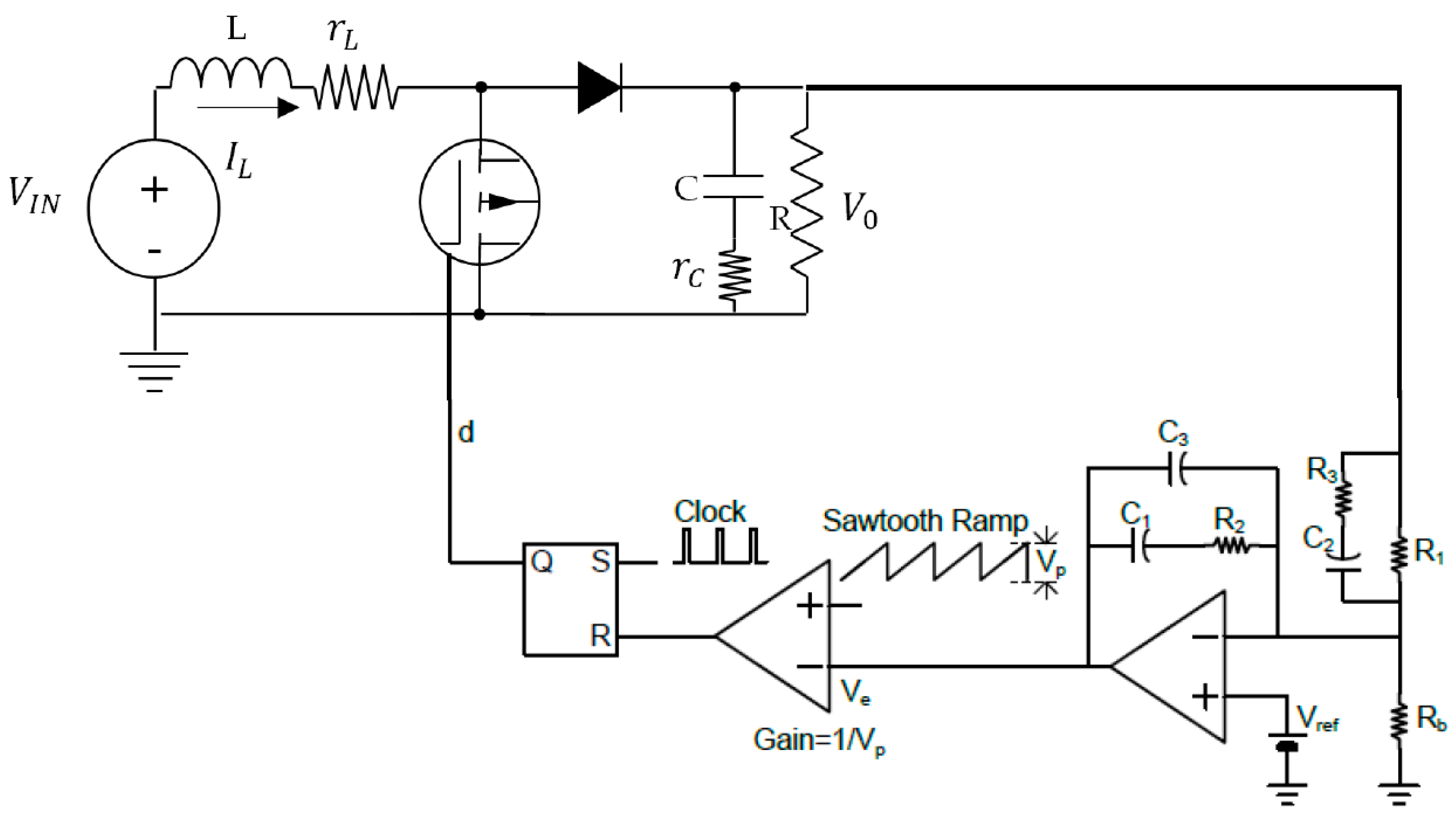
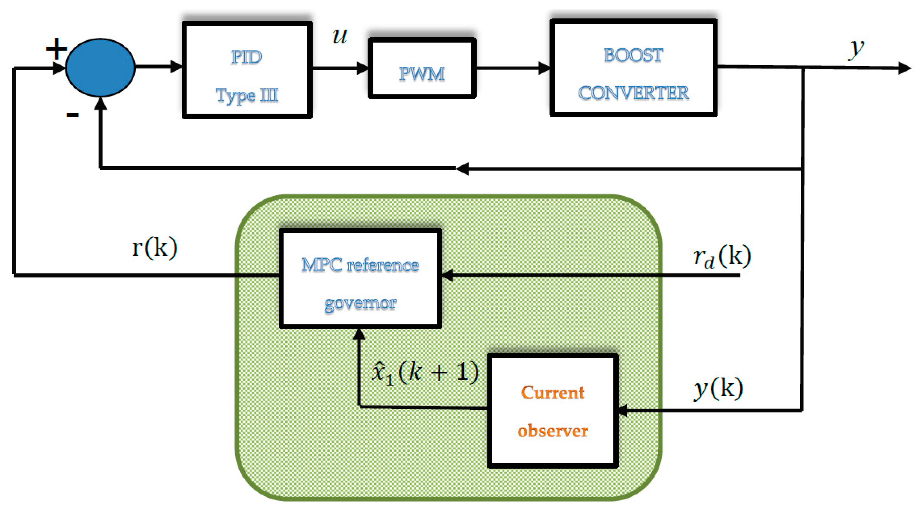
4. MPC Reference Governor Design for a Voltage-Mode-Controlled Converter

The development of an optimal and efficient reference governor using linear MPC ideas is commonly performed in a linear discrete-time state-space formulation. Hence, both the system and Type III controller dynamics have to be modeled in an appropriate linear discrete-time state-space form. To this end, a similar procedure to the one in [1] was followed.

4.1. Converter State-Space Modeling

An accurate state-space model of the boost circuit of Figure 1 can be found by following the common practice of defining the inductor’s current x 1 = I L and the capacitor’s voltage x 2 = V 0 as state variables. The model takes the following bilinear form (the tiny resistance r C is ignored for simplicity):
x ˙ = A x + B u + F 1 x 1 u + F 2 x 2 u + B v , y = C x , x = [ I L   V 0 ] T R 2 × 1 A = [ r L L 1 L 1 C 1 R C ] , B = 0 , C = [ 0   1 ] T , F 1 = [ 0   1 C ] T , F 2 = [ 1 / L   0 ] T ,   B v = [ V I N / L   0 ] T
The next step is to linearize the dynamics about the equilibrium point using small signal variations reflecting nominal operating conditions x ˜ = x x e , u ˜ = u u e , y ˜ = y y e to obtain new matrices:
x ˜ ˙ = A l i n   x ˜ + B l i n u ˜ , y = C l i n   x ˜ + D l i n u ˜ A l i n = [ r L / L ( 1 u e ) / L ( 1 u e ) / C 1 / ( R C ) ] , B l i n = [ x 2 e / L x 1 e / C ] T , C l i n = [ 0   1 ] T , D l i n = 0 x e = [ x 1 e     x 2 e ] T , x 1 e = V I N r L + R   ( 1 u e ) 2 , x 2 e = ( R   V I N   ( 1 u e ) ) / ( r L + R   ( 1 u e ) 2 )
These linear continuous-time dynamic equations may be further discretized for a fixed sampling period T to obtain the following discrete-time model in the new state variables x d R 2 × 1 :
x d ( k + 1 ) = A d   x d ( k ) + B d   u d ( k ) ,   y d ( k ) = C d   x d ( k ) A d = e A l i n   T ,   B d = 0 T e A l i n   τ   Β   d τ ,   C d = C

4.2. PID Controller State-Space Form

A reliable discretization method for small sampling periods is the approximate backward difference (It is well known that, for a sufficiently high sampling frequency, all approximation methods are safe and guarantee satisfactory performance. However, the backward difference method is the simplest possible representation and hence advantageous for subsequent modeling and control design.) method, for which it is well known that the Laplace-transform variable s and the Z-transform z are related by = z 1 T z as the time derivative of a time variable x ( t ) is approximated by x · ( t ) = x ( k ) x ( k 1 ) T . Direct substitution of s in the Type III controller transfer function G P I D ( s ) as in (3) leads to the following discrete-time transfer function G P I D ( z ) :
G P I D ( s ) = k P I D s ( 1 + s ω Z C ) 2 ( 1 + s ω P C ) 2   s = z 1 Tz G P I D ( z ) = K 0 z   ( z z 1 ) 2 ( z 1 ) ( z z 2 ) 2 K 0 = k P I D   T   ( 1 + α ) 2 ( 1 + β ) 2 ,   z 1 = α 1 + α ,   z 2 = β 1 + β ,   a = 1 T ω Z C ,   β = 1 T ω P C
Subsequently, a state-space formulation is obtained by partial fraction expansion of G P I D ( z ) as
G P I D ( z ) = K 0 z   ( z z 1 ) 2 ( z 1 ) ( z z 2 ) 2   = K 0 + K 1 z 1 + K 2 z z 2 + K 3 ( z z 2 ) 2 K 1 = K 0 ( z 1 1 ) 2 ( z 2 1 ) 2 , K 2 = K 0 2 z 2 3 ( 3 + 2 z 1 ) z 2 2 + 4 z 1 z 2 z 1 2 ( z 2 1 ) 2 , K 3 = K 0 z 1 2 z 2 2 z 1 z 2 2 + z 2 3 z 2 1
Further introduction of a new controller state variable vector x c = [ x c 1 , x c 2 , x c 3 ] T R 3 × 1 as
X c 1 ( z ) = K 1 z 1 , X c 2 ( z ) = K 2 z z 2 , X c 3 ( z ) = K 3 ( z z 2 ) 2
This leads, after some trivial calculations, to a simple state-space formulation in discrete-time:
x c ( k + 1 ) = A c   x c ( k ) + B c   u c ( k ) ,   y c ( k ) = C c   x c ( k ) + D c   x c ( k ) A c = [ 1 0 0 0 z 2 0 0 1 z 2 ] ,   B c = [ 1 1 0 ] ,   C c = [ K 1 , K 2 , K 3 ] T ,   D c = K 0

4.3. Reference Governor MPC Design and Tuning

For an MPC reference governor design on top of an already controlled plant, a discrete-time state-space model of the combined converter–controller closed-loop system is required. This may be found by noting that the output of the controller is the input to the converter, i.e., y c ( k ) = u d ( k ) , and that the input of the controller u c ( k ) is the error e ( k ) = r ( k ) y ( k ) ; hence, an augmented system-controller closed-loop discrete-time state-space formulation may be formed with a new extended state vector x a = [ x c   x d ] T   R 5 × 1 and corresponding matrices from (9), (13) as follows:
x a ( k + 1 ) = A a   x a ( k ) + B a   r ( k ) ,   y a ( k ) = C a   x a ( k ) A a = [ A c B c C d B d C c A d B d D c C d ]   R 5 × 5 ,   B a = [ B c B d D c ] R 5 × 1 ,   C a = [ 0   C d ] T   R 1 × 5
It is important to note that, in this formulation, the input coincides with the reference signal r ( k ) , while the output y a ( k ) coincides with the real output of the system, i.e., the output voltage V 0 . The role of the reference governor is explained pictorially in Figure 3. It is a secondary controller responsible for producing a dynamically modified optimal reference signal r ( k ) from a desired set-point signal r d ( k ) , which is usually constant or at least slowly time-varying. The MPC reference governor is using the measured (sampled) output y ( k ) to extract knowledge of the full state vector x a ( k ) . There are five state variables, which are all known except the inductor current for which a specialized observer is included, as explained below in Section 4.4. The MPC scheme operates by resorting at the linear closed-loop model in (14) to predict future trajectories and generate optimal decisions for r ( k ) . This scheme can be combined either with an analogue Type III compensation circuit (Figure 2) or with a purely digital implementation, as implied by Figure 3.
One of the simplest possible and computationally tractable ideas for an MPC formulation was adopted in this work, along the same lines with relevant design in [1], which proved surprisingly effective as the simulations results reveal in the next sections. An unconstrained formulation was used, which allowed the derivation of an explicit form of the corresponding MPC control law, hence avoiding the computationally demanding on-line optimization procedures. The gains of the controller were fixed and a priori determined, and this resulted in a computationally tractable implementation, especially because it is a single-input and single-output (SISO) system with low control and prediction horizon demands. Simple constraints regarding the size or the rate of change of the controller’s signal can also be dealt with easily with the same explicit MPC formula and without compromising the optimality, as explained in the sequel.
The first observation is that our MPC reference governor controller must be equipped with an extra integrator because the controller’s decisions for r ( k ) must converge to the desired values r d ( k ) . The simple formulation in ([24], Chapter 1) was adopted, where an embedded integrator augmented state-space model was used for control design and optimization.
The first step was to take a difference operation on both sides of (14) to obtain the following:
Δ x a ( k + 1 ) = A a   Δ x a ( k ) + B a   Δ r ( k )
where the differences of the control variables and the input need to be defined as follows:
Δ x a ( k + 1 ) = x a ( k + 1 ) x a ( k ) ,   Δ r ( k + 1 ) = r ( k + 1 ) r ( k )
A new extended state vector x ( k ) R 6 × 1 was formed next with an embedded integrator:
x ( k ) = [ Δ x α ( k ) T   y ( k ) ] T
Combining (16) and (17) yielded a new state-space model of an increase by one order given by the following equation:
x ( k + 1 ) = A   x ( k ) + B   Δ r ( k ) ,   y ( k ) = C   x ( k ) A = [ A a 0 5 T C a A a 1 ]   R 6 × 6 ,   B = [ B a C a B a ] R 6 × 1 ,   C = [ 0 5   1 ] T   R 1 × 6 , 0 5 = [ 0 , 0 , 0 , 0 , 0 ]
Note that the input to the new state-space model ( A , B , C ) is now Δ r ( k ) . Assuming that, at the sampling instant k i > 0 , the state variable vector x ( k i ) is available and the control horizon is N c , the future control trajectory is given by the sequence Δ r ( k i ) ,   Δ r ( k i + 1 ) , , Δ r ( k i + N c 1 ) . Moreover, for a prediction horizon (optimization window) N p , the future state variables are specified as x ( k i + 1 ) ,   x ( k i + 2 ) , , x ( k i + N p ) . The model equation in (18) can be sequentially applied to yield the future state and output variables as a function of the future control parameters (for a detailed exposition see [24]). By defining the vectors
Δ R =   [ Δ r ( k i ) ,   Δ r ( k i + 1 ) , , Δ r ( k i + N c 1 ) ] T ,   Y =   [ y ( k i + 1 ) ,   y ( k i + 2 ) , , y ( k i + N p ) ] T
which have dimensions N c ,   N p in the SISO case, respectively, all prediction equations can be collected in a compact matrix form as follows:
Y = F   x ( k i ) + Φ   Δ R F =   [ C A ,   C A 2 , C A 3 , , C A N p ] T ,   Φ = [ C B B 0 0 C A B C B 0 0 C A 2 B   C A B C B 0 C A N p 1   B C A N p 2   B C A N p 3   B C A N p N c   B ]
Assuming that the setpoint signal r d ( k i ) at sample time k i is constant in the optimization window, the data vector containing the setpoint data is R d T = [ 1   1   1 ] N p r d ( k i ) = R ¯ d r d ( k i ) , and the cost function J to be minimized is the sum of two terms:
J = ( R d Y ) T ( R d Y ) + Δ R T R ¯ Δ R
where the first term is related to the tracking errors and the second to the size of Δ R , while the weighting matrix R ¯ = r w I N c × N c is a diagonal matrix, with r w 0 the main tuning parameter affecting closed-loop performance. By zeroing the first derivative of J , the unconstained optimal solution for the control problem is given as follows (assuming that Φ T Φ + R ¯ is invertible):
Δ R = ( Φ T Φ + R ¯ ) 1 Φ T ( R ¯ d r d ( k i ) F   x ( k i ) )
Due to the receding horizon principle, only the first element Δ r of Δ R at time k i is applied:
Δ r ( k i ) = K r · r d ( k i ) K x · x ( k i )
where K r is the first element of ( Φ T Φ + R ¯ ) 1 Φ T R ¯ d , and K x is the first row of ( Φ T Φ + R ¯ ) 1 Φ T F . Hence, the optimal MPC reference governor takes an explicit static state-feedback form, where the gains of the controller are fixed and can be a priori determined. This is important for a computationally tractable implementation. Moreover, as we have a SISO system, simple constraints regarding the size of r ( k i ) and/or the rate of change Δ r ( k i ) of the reference signal can also be dealt with easily with the same explicit MPC formula and without compromising the optimality. This is explained in ([24], Chapter 3). When constraints are violated, the only action needed is to clamp the imposed r ( k i ) at the limit and notify the observer accordingly. These simple constraints are of the following form:
Δ r m i n Δ r ( k i ) Δ r m a x ,   r m i n r ( k i ) r m a x

4.4. Nonlinear Current Observer

The implementation of the MPC scheme introduced in the previous section requires knowledge of all five state variables in x a = [ x c   x d ] T   R 5 × 1 , which include the inductor current x 1 = I L . To avoid the addition of an extra current sensor, an efficient current observer can be a good alternative. In [1], a general linear observer (Kalman filter) was employed. In this work, a recently proposed robust and efficient nonlinear current observer [25] was selected with very good results due to its specialized nonlinear structure as well as the high sampling frequency used. A brief description of this structure is given below; for more details, please refer to [25].
With reference to the bilinear formulation of the converter dynamics as in (7), the observer formula proposed in [25] for the estimated state vector x ^ = [ x ^ 1   x ^ 2   ] T   R 2 × 1 based on the output estimation error x ˜ 2 = x ^ 2   x 2 (recall that x 2 = V 0 is the output voltage directly measured) is given by the following continuous-time equations:
x ^ ˙ = A   x ^ + F 1 x ^ 1 u + F 2 x ^ 2   u + B v + W ( x 2 , x ˜ 2 ) W ( x 2 , x ˜ 2 ) = [ 0 K x ˜ 2 + η ( x 2 , x ˜ 2 ) ] ,   η ( x 2 , x ˜ 2 ) C 1 s g n ( x ˜ 2 ) ( ρ   | x 2 | + a )
In this formula, the value of the parameter ρ is determined by the a priori assumed perturbation bounds of the unknown load R . The tuning parameters are K , a . After some experimentation with the tuning suggestions in [25], appropriate values K = 1 ,   a = 10 4 were found for ρ = 0.1 (corresponding to load resistance R in the designated range 10–50 Ω).
The observer was tested numerically in a discrete-time formulation using the backward difference method for approximating the derivatives in (25). The difference update equations used take a straightforward form that can be directly coded to a microprocessor in the following form:
x ^ 1 ( k + 1 ) = x ^ 1 ( k ) + T · [ r L L 1 x ^ 1 ( k ) L 1 x ^ 2 ( k ) + L 1 x ^ 2 ( k ) u ( k ) + V I N L 1 ] x ^ 2 ( k + 1 ) = x ^ 2 ( k ) + T · [ C 1 x ^ 1 ( k ) R 1 C 1 x ^ 2 ( k ) C 1 x ^ 1 ( k ) u ( k ) K x ˜ 2 ( k ) + η ( k ) ] η ( k ) = C 1 s g n ( x ˜ 2 ( k ) ) ( ρ   | x 2 ( k ) | + a )

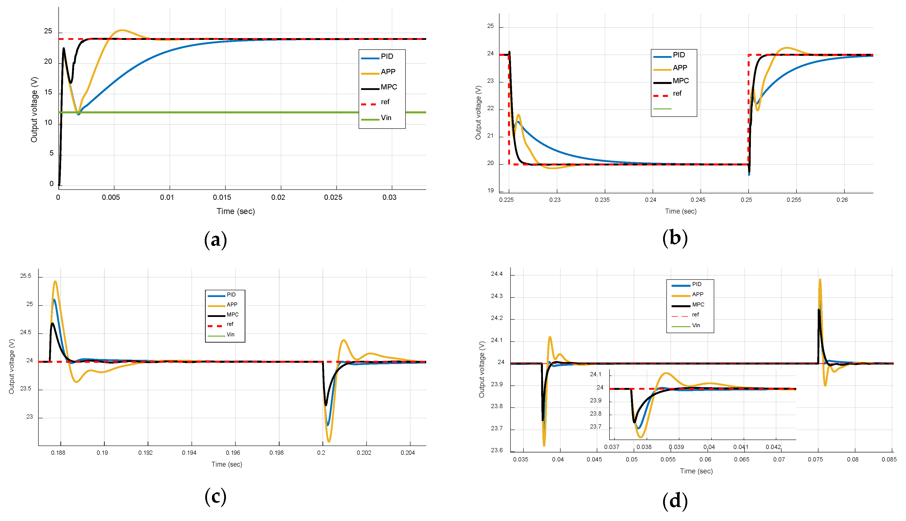
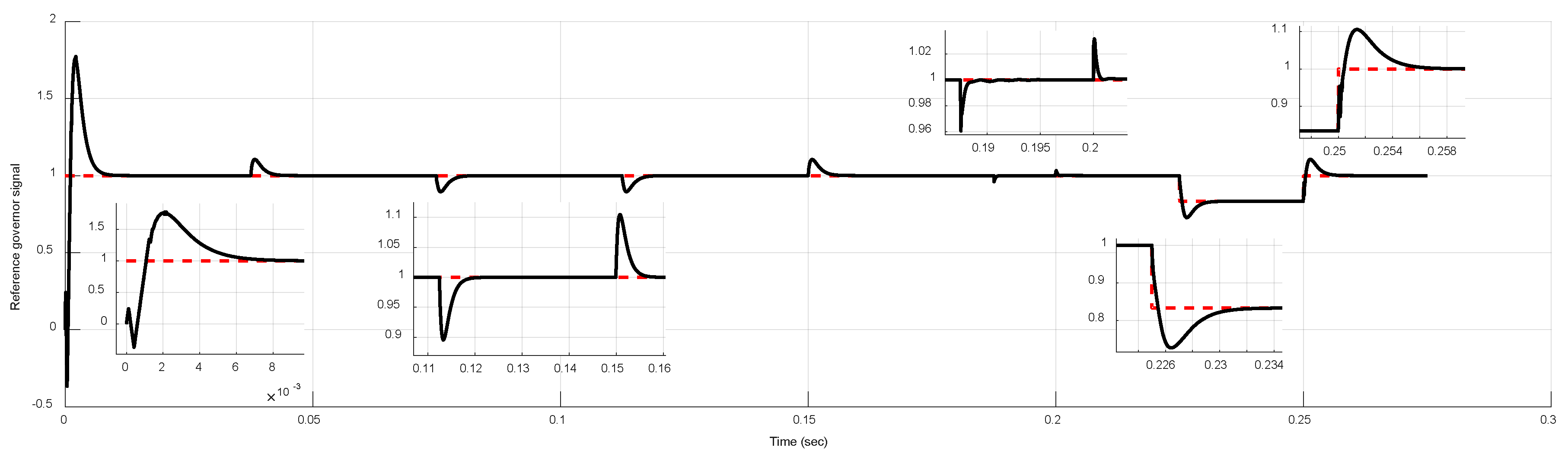
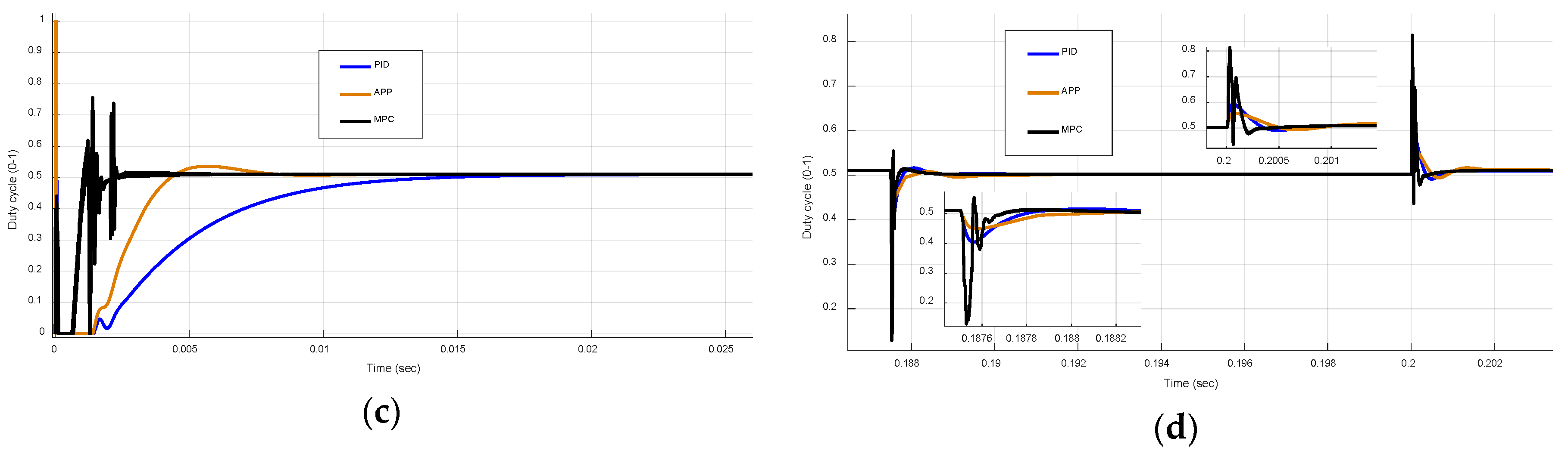
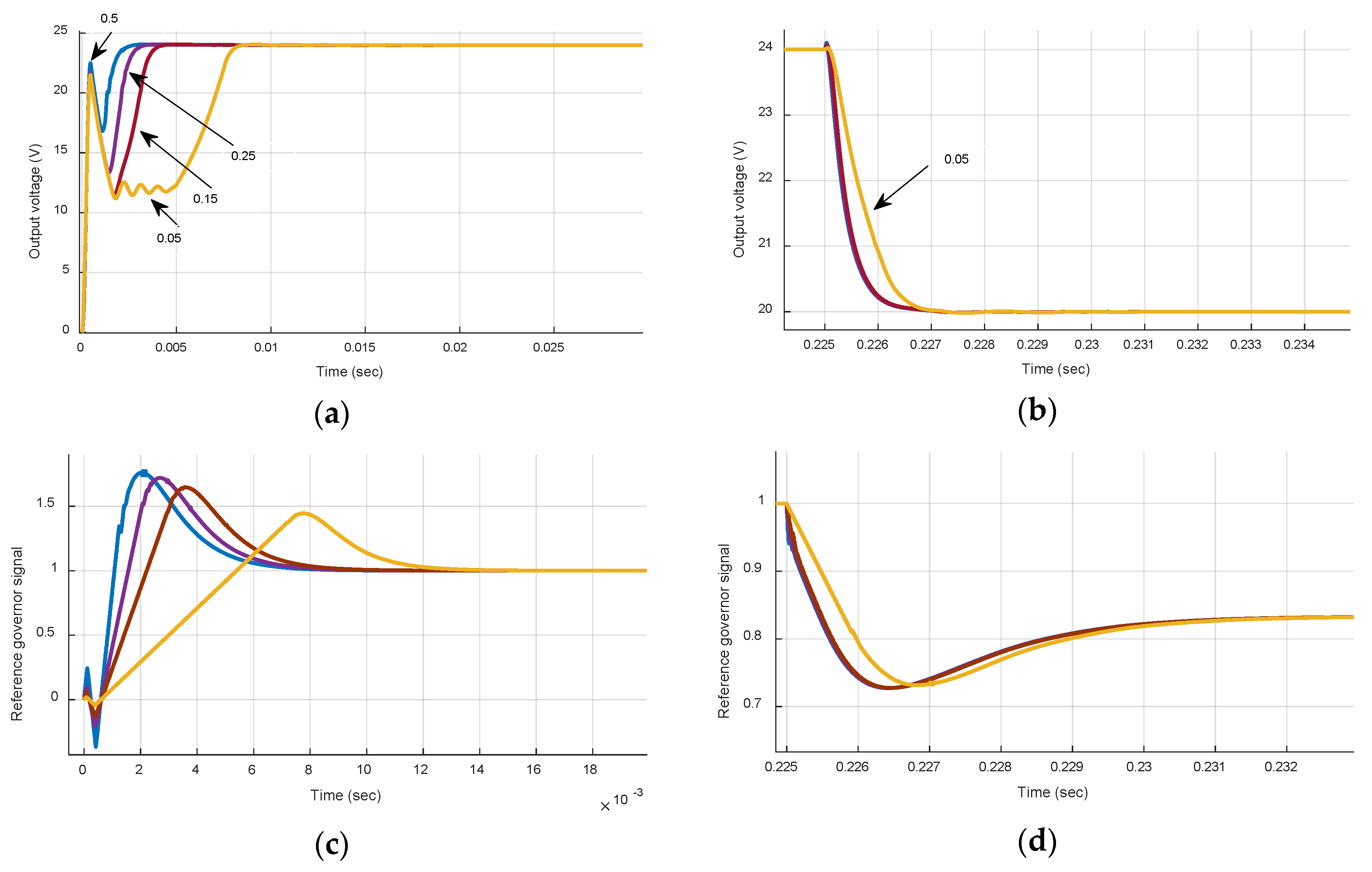
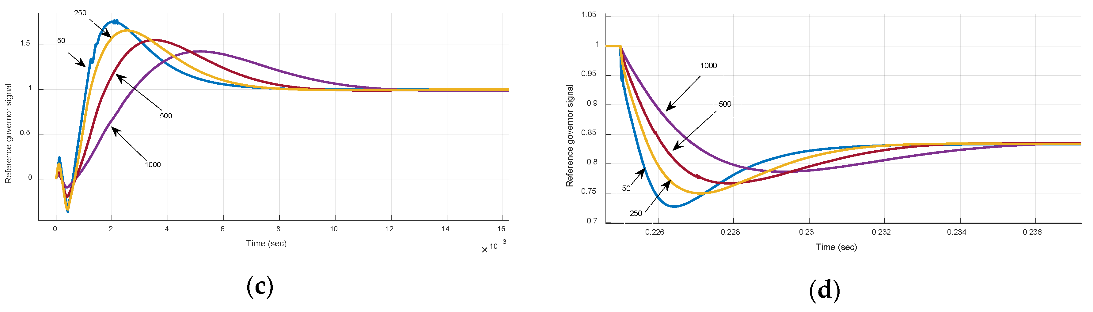
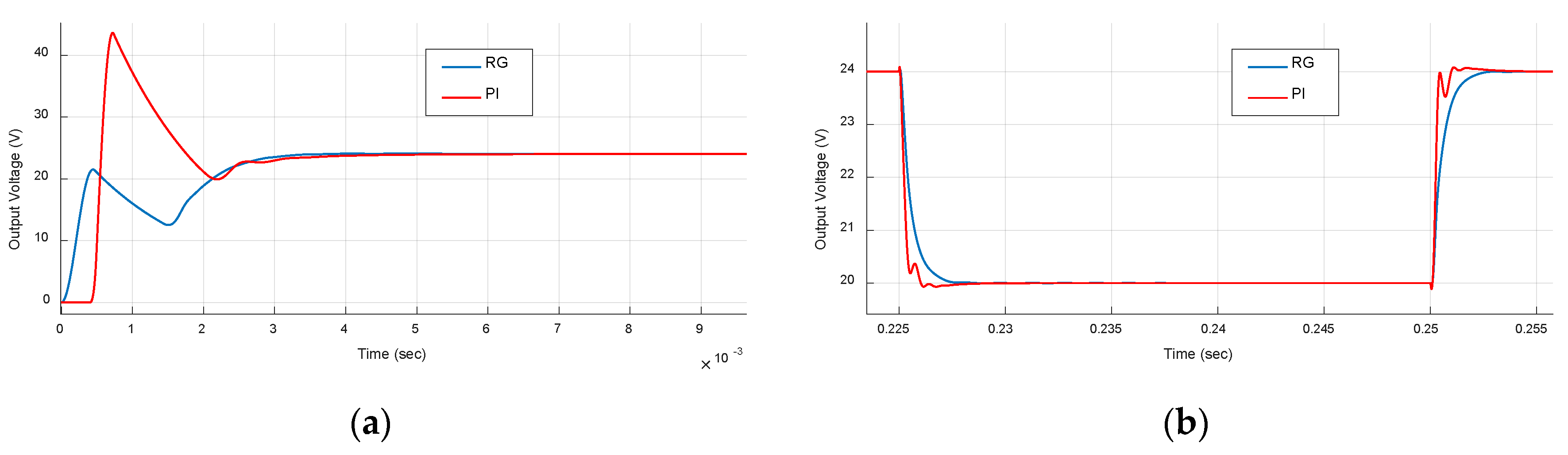
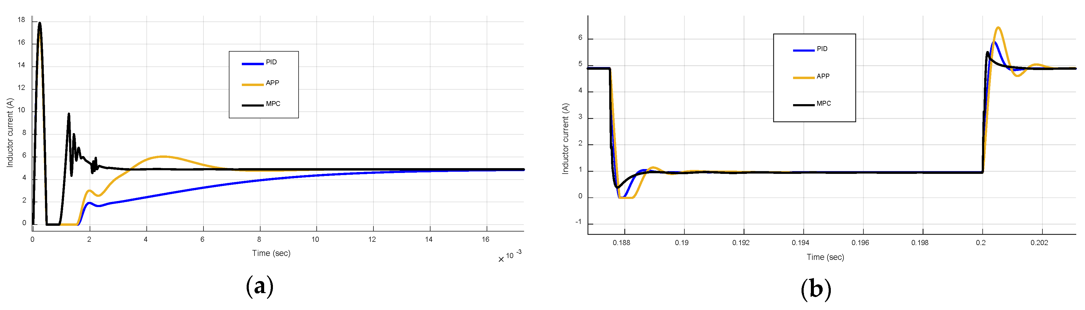
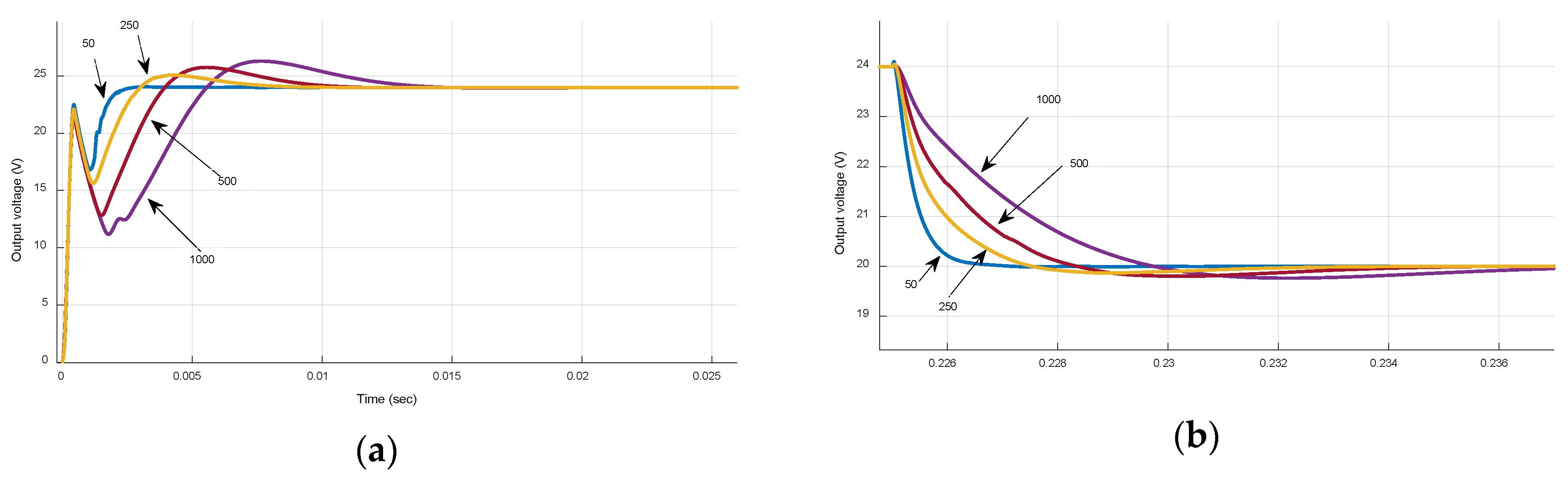
5. Numerical Simulation Results

In this section, the performance enhancement achieved with the proposed MPC reference governor is presented with the help of Figure 4, Figure 5, Figure 6, Figure 7 and Figure 8. A detailed comparison with the two controllers used in [22] was made, where the distinctive features of all schemes were revealed. The simulations were performed in two environments: in Simulink with the help of the PowerSim library, which uses the exact switching model, and in MATLAB with the nonlinear averaging model in discrete-time with sampling frequency equal to the switching frequency f s = 200 kHz . For such a high sampling frequency, the results obtained by both methods are very close to each other; however, the advantage of the second method is that it contains transparent code (close to microprocessor level) that runs significantly faster and also produces clearer diagrams for comparison purposes. Hence, a decision was made to present these results in the following figures.
It is noted that a lower sampling frequency is enough for a successful reference governor scheme. A frequency of 100   kHz , i.e., equal to half of the main controller sampling frequency, was used for the MPC scheme when obtaining the results shown below. The specifications of the MPC reference governor scheme are given in Table 2. While experimenting with different values for the control and prediction horizons, we realized that we could afford to reduce the control horizon N c to unity as long as the prediction horizon was long enough to deal with the nonminimum phase characteristic of the transient responses of the boost converter. The values N c = 1 , N p = 45 were found suitable in order to obtain very satisfactory results.
Figure 4 compares the performance of the three controllers in four different cases covering the most important situations, i.e., startup transient, reference input changes, load perturbations, and line voltage changes. The notation used is as follows: the MPC reference governor scheme on top of the Type III controller is denoted as MPC, the combination of ROAPFPC with the Type III is called APP (ARMarkov Plus PID), while the Type III controller alone is termed as PID.
It is clear from Figure 4a,b that APP was 3–4 times faster than PID when it came to reference tracking, and it is clear from Figure 4c,d that APP was slightly worse than PID as far as disturbance rejection (load or input voltage changes) was concerned. It is also evident that the proposed strategy in this work, i.e., MPC, outperformed both APP and PID in all four situations, as depicted in Figure 4, where it appeared to be at least two times faster in terms of rise time and three times faster in terms of settling time, approximately.
The key to achieving this performance enhancement was the dynamic modification of the reference input by which the Type III controller was commanded. The command history corresponding to all four cases of Figure 4 is shown in Figure 5, where the values are normalized to unity for better illustration.
Further details of the three control laws for the first two cases (startup and reference changes) are given in Figure 6. The inductor current and duty cycle waveforms (i.e., the main control signals) reveal that the performance benefits obtained were not due to higher absolute values of currents or duty cycles or extensive use of energy but rather to a smarter use of the available energy, which was characterized by higher variability. The MPC controller appeared to act in a much more flexible manner, allowing large excursions of the control signals in a short time scale, without imposing extra operational requirements, e.g., higher inductor currents or energy consumption or excessive duty cycles. In fact, in MPC, the maximum current imposed did not increase, while the duty cycle never came close to saturation.
Further justification of this claim is provided by the simulation results depicted in Figure 7. Four different responses were obtained by imposing different rate constraints Δ r m a x = 0.05, 0.15, 0.25, 0.5, as in (24), which restrict the flexibility of the dynamically modified reference governor signals. Although there was little effect when considering perturbations around the nominal working point, it was obvious that, during the startup, they played a crucial role in the performance enhancement that may be achieved. Nevertheless, it was clear that in all cases the MPC controller inevitably did a good job, at least within the imposed constraints envelope.
Finally, a last test was performed to assess the proper MPC operation; a set of different weighting factor values r w (50, 250, 500, 1000) were used, and the comparative results are shown in Figure 8. The controller behaved exactly as expected, i.e., larger r w values gave rise to more sluggish responses, which also exhibited increased overshoot. The values r w = 50, Δ r m a x = 0.5 were the ones selected for the nice results shown in Figure 4, Figure 5 and Figure 6. The explicit MPC gains in (21) are given next:
K r = 0.1737 ,   K x = [ 0.0001535 0.064 0.0847 1.2691 5.3893 0.1737 ] T

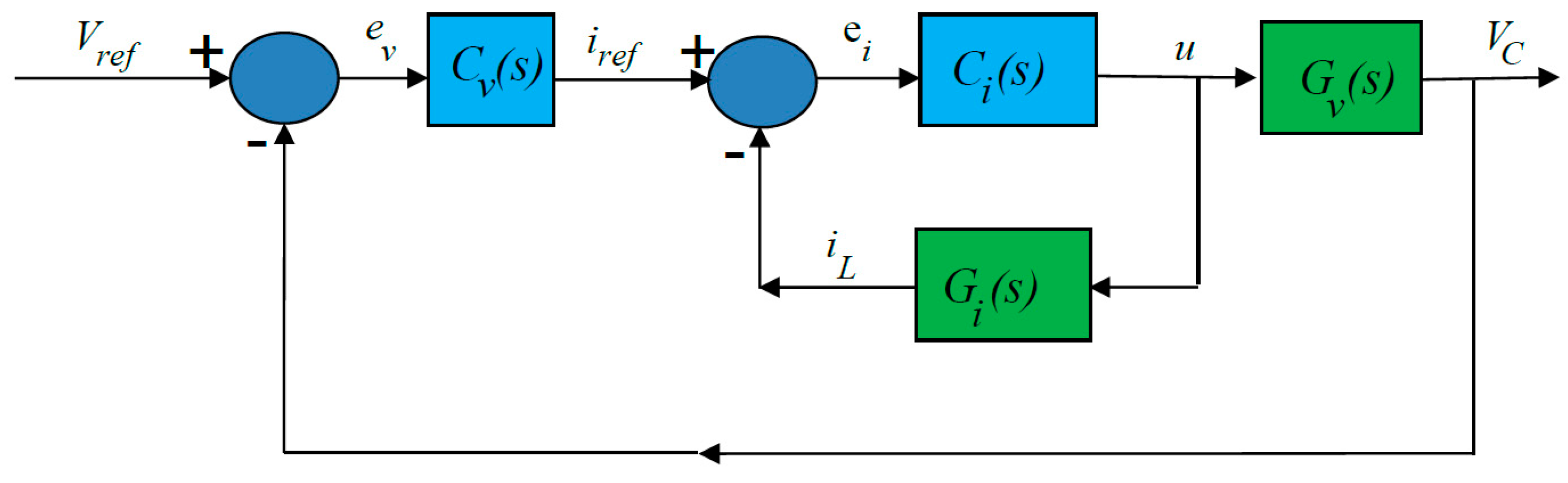
6. MPC Reference Governor Design for a Two-Loop Current-Mode-Controlled Converter

The developments in the previous sections considered a voltage mode control (VMC) structure, which consists of a single loop for output voltage regulation. This simplifies the control structure because the use of a current sensor is avoided, but it requires a more complicated controller (Type III). The alternative for simplifying the converter’s dynamics and the controller form is to adopt the so-called current mode control (CMC) structure, which takes a two-loop cascaded form, resulting in an indirect linear control approach in the analog [26] or the digital domain [27]. The main advantage is that the current/voltage dynamics may be separated, and simple PI controllers for each loop may be designed using trivial pole placement procedures, which simplifies the control task while also ensuring faster transient response. The shortcoming is the need for a current sensor. The cascaded two-loop scheme used for analog design [26] is shown in Figure 9.
An averaged current-mode structure is followed, which involves the design of two nested control loops with a current (inner loop) controller C i ( s ) and a voltage (outer loop) controller C v ( s ) . The transfer functions G i ( s ) = I L ( s ) U ( s ) ,   G v ( s ) = V C ( s ) U ( s ) are given based on the linearization of (8) as follows:
G i ( s ) = u e x 1 e + x 2 e / R r L / R + u e 2   C x 2 e / ( u e x 1 e + x 2 e / R )   s + 1   L C r L / R + u e 2   s 2 + L / R + r L C r L / R + u e 2 s + 1 G v ( s ) = u e x 2 e x 1 e r L r L / R + u e 2   L / ( u e x 2 e / x 1 e r L )   s + 1   L C r L / R + u e 2   s 2 + L / R + r L C r L / R + u e 2 s + 1
where u e = 1 u e and the presence of a right-half plane zero in G v ( s ) (which is not affected by the control law) dictates the design procedure. For dynamics separation between the two loops, the inner loop’s bandwidth must not be placed near this zero; otherwise, the designed performance cannot be guaranteed. The desirable dynamic performance of the faster inner loop is imposed first by appropriate pole placement on the basis of certain bandwidth and damping features. The control design of the outer loop follows after closing the inner loop and designing the slower outer loop to be at least 5 times slower than the inner closed loop [26]. Trivial PI controllers are sufficient for both designs, where a simple root locus procedure can be used to establish the dominant pole’s position.

6.1. Two-Loop PI Controller State-Space Form

Again, we adopt the backward different method for which a PI control law C P I ( s ) = K p + K i / s with gains K p ,   K i is approximated in dicrete-time by C P I ( z ) = ( K p + K i T ) z K p z 1 . This is a first-order equation admitting a simple state-space formulation. For the two PI control laws in Figure 9, by assuming gains K p 1 ,   K i 1 for the inner law C i ( z ) , gains K p 2 ,   K i 2 for the outer law C v ( z ) , and by defining corresponding state (integrator) variables x i ,   x v , and a controller state variable vector x c = [ x i , x v ] T R 2 × 1 , new state equations are obtained:
x i ( k + 1 ) = x i ( k ) + u i ( k ) ,   y i ( k ) = K I 1   x i ( k ) + K P I 1   u i ( k ) x v ( k + 1 ) = x v ( k ) + u v ( k ) ,   y v ( k ) = K I 2   x i ( k ) + K P I 2   u i ( k )
where the inputs u i , u v and the outputs y i , y v of the PI blocks in Figure 8 are specified as follows:
u i = e i = i r e f i L = i r e f y v   , u v = e v = V r e f V C , y i = u   , y v = i r e f
and the new gains are defined as K I 1 = K i 1   T ,   K I 2 = K i 2   T ,   K P I 1 = K p 1 + K i 1   T , K P I 2 = K p 2 + K i 2   T .

6.2. Current-Mode Reference Governor MPC Formulation

Similarly to Section 4.3, for an MPC reference governor an augmented system-controller closed-loop discrete-time state-space formulation is formed with a new extended state vector x a = [ x c   x d ] T   R 4 × 1 and corresponding matrices from (9) and (29) as follows:
x a ( k + 1 ) = A a   x a ( k ) + B a   r ( k ) ,   y a ( k ) = C a   x a ( k ) A a = [     1     K P I 2   1   K I 2   0   1   0   1 A d 1 K P I 1 B d   A d 2 K P I B d   K I 1 B d   K P I 1 K I 2 B d ] ,   B a = [ K P I 2 1 K P I   B d ] ,   C a = [ 0   C d ] T
where K P I = K P I 1   K P I 2 and A d 1 ,   A d 2 are the two columns of A d in (9). This result can be obtained after simple algebraic manipulations by noting that the controller/converter connection is established by the relations u v = r x d   ( 2 ) ,   y i = u . Compared to the voltage-mode-controlled system (14), it is noted that the current-mode-controlled one is lower order due to the simpler second-order controller (two PI controllers) as opposed to the third-order controller of the Type III scheme.

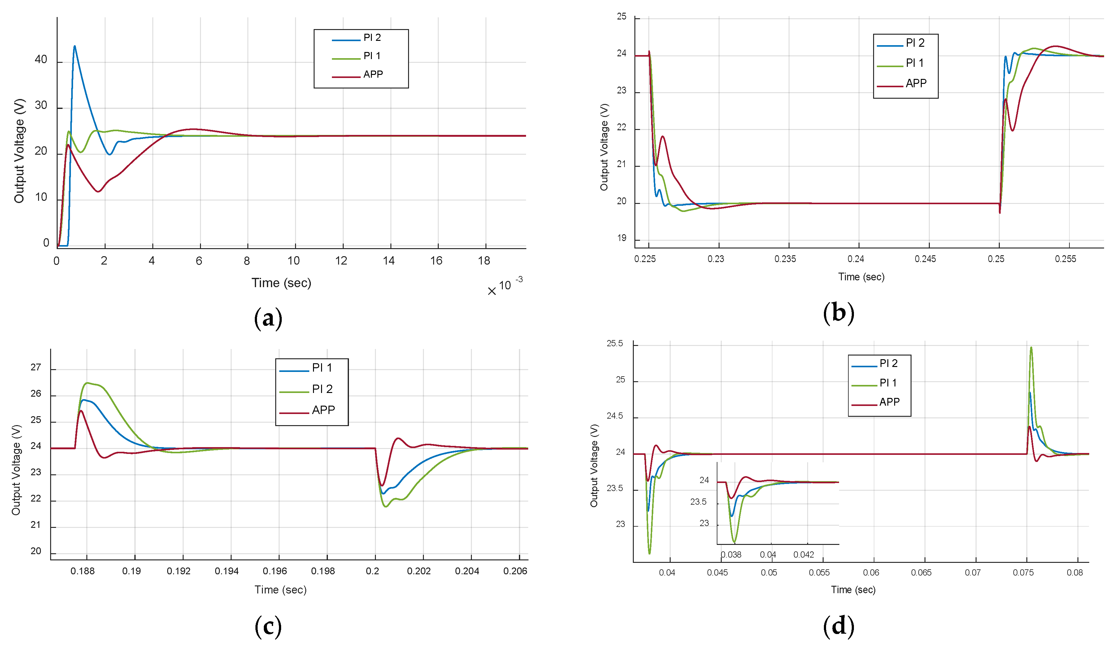
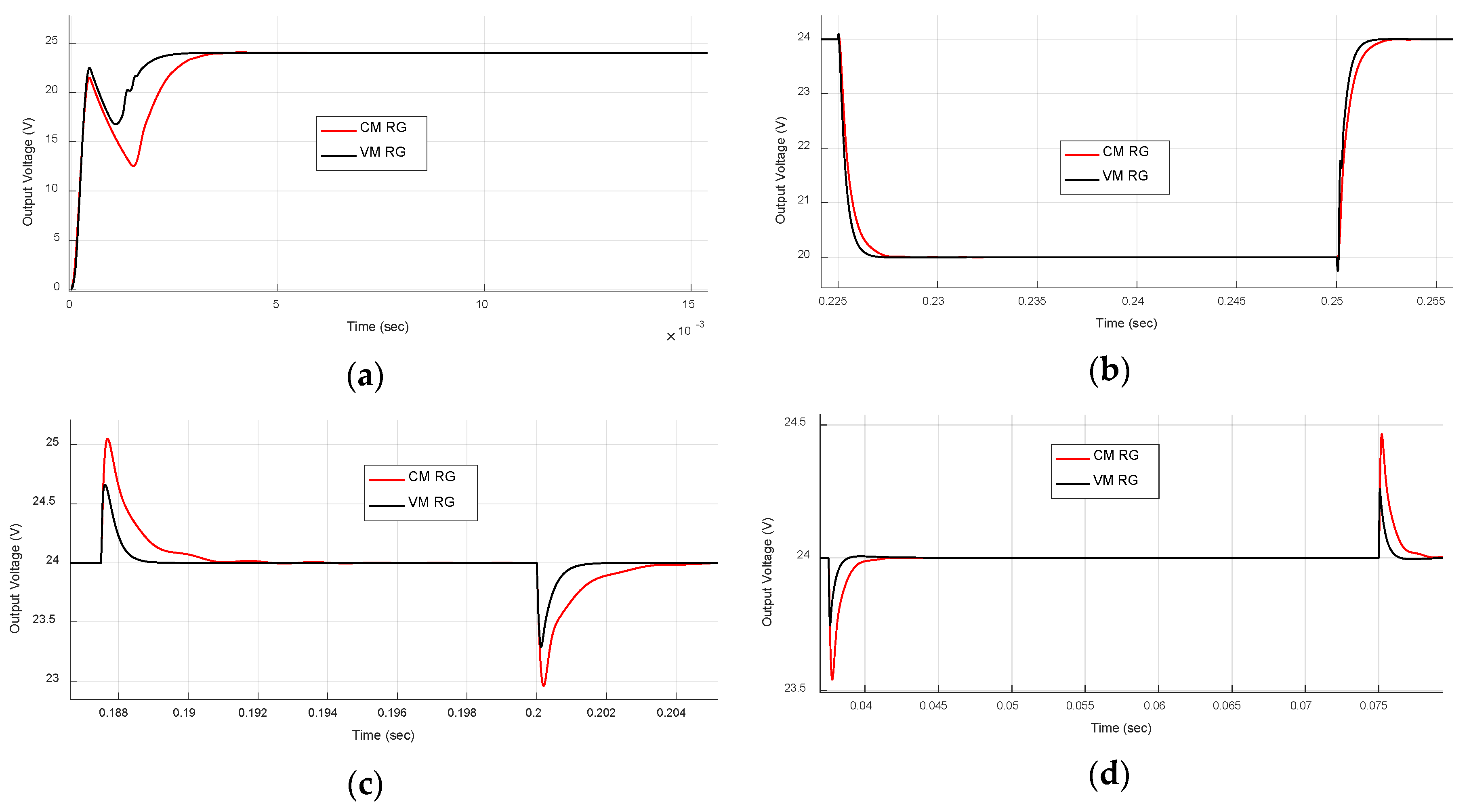
6.3. Numerical Simulation Results

Following the guidelines of the previous sections, two different current-mode designs were performed, with the specifications given in Table 3. The first design (PI 1) had smaller bandwidth (settling time T s of 3 ms) and notably smaller gains compared to the second (PI 2). The transient responses of these two-loop PI current-mode designs with the APP (PID + ROAPC) design of Section 3 are compared in all possible situations in Figure 10.
Figure 10a,b confirms the reference tracking of superior performance of the current-mode control, while Figure 10c,d shows its inferior disturbance rejection properties. This is expected as current-mode control exploits the faster current dynamics in the inner loop, while PID control offers better disturbance rejection. Using higher gains, as in PI 2, offers some improvements; however, it also results in a startup transient with unacceptably high overshoot, which requires some form of soft-start procedure. Can a reference governor scheme offer any remedies to these situations? This question is answered with the results shown in Figure 11 for the PI 2 design. The disturbance rejection was drastically improved, while the reference tracking problem in the startup was tackled. The MPC current-mode reference governor specifications for obtaining the results of Figure 11 are listed in Table 4.
Finally, this MPC current-mode reference governor (CM RG) design was compared with the corresponding voltage-mode reference governor (VM RG) design of Section 5, in Figure 12. The two designs had comparable reference tracking capabilities, while VM RG had better disturbance rejection properties. This was attributed to the PID Type III controller around which the VM RG was designed and the important fact that the relatively inferior reference tracking properties of the PID Type III controller were cured using a VM RG. All in all, the merits of combining an optimal MPC RG scheme in voltage-mode with a typical PID Type III controller have become obvious. The best results in terms of reference tracking and disturbance rejection were obtained without the need to resort to a current-mode two-loop policy, which is also less efficient with disturbance rejection.

7. Conclusions

This article presents one of the first attempts in the literature to apply reference governor ideas to the power electronics field for obtaining performance enhancements without replacing the main controller, which may be worth keeping for a cheap and/or safe modern implementation. Assuming that a digital microprocessor can be integrated into the existing control circuit, a secondary controller in the form of a reference governor that dynamically modifies the set-point of the primary controller may be a good idea, provided the implementation cost and complexity are kept low.
More specifically, this research considered the problem of enhancing the performance of boost DC–DC converters that are precompensated in voltage-mode or current-mode by a typical primary controller such as a Type III (or a double PI for current-mode), which is a standard industrial practice. A secondary controller–prefilter in the form of a reference governor was systematically designed, which operates by introducing dynamic adjustments to the imposed voltage reference input signal. It was shown that such a scheme, designed optimally via a simple linear MPC methodology, can enhance the performance in a wide operating range without imposing extra requirements or limitations. Clear improvements compared to recently reported results in the literature were found. It is noteworthy that even for such a highly nonlinear (bilinear) and nonminimum phase system like a boost converter, the shortcomings of a linear controller like PID, which is designed with a linear model for a particular operating point, can be dealt with by complementing it with a relatively simple linear unconstrained MPC scheme that takes a simple explicit form.
It is quite common to use current-mode two-loop controllers for nonminimum phase boost converters as they offer some advantages. Our simulation results revealed that the voltage-mode MPC RGs outperformed the current-mode designs, especially in disturbance rejection situations. Current-mode MPC RGs were also tested, which offered some improvements; however, voltage-mode MPC RGs combined with PID Type III primary controllers delivered the best results while also avoiding the use of a current sensor.
Of course, these advancements come at a price. The proposed controller is more complicated as it is expressed in a state-space form, and it requires extra knowledge of the inductor current and a digital microprocessor implementation. However, the computational demands of the proposed scheme are light enough and can be addressed with a modern cheap microprocessor. Moreover, placing an inductor current sensor is not necessary as reliable nonlinear observers for bilinear systems are available.
A light MPC algorithm with short horizons and trivial constraints, allowing an explicit solution through unconstrained optimization, was proven to be sufficient enough for our main purpose in the present work. These first positive results pave the way for further research with a reference governor flavor in the area of power electronics, e.g., in more complicated converter topologies or using more advanced techniques. Only few possibilities offered by MPC technology were explored in this research. There is a multitude of methods in the literature that are worth testing, including many more sophisticated constrained linear or nonlinear MPC schemes. The vast literature in MPC techniques, as well as the various optimal reference governor ideas developed thus far, imply that many other constrained optimization methodologies are available to be explored for future improvements.

Funding

This research received no external funding.

Acknowledgments

Research supported by the Centre for Research and Technology Hellas (CERTH)/ Chemical Process and Energy Resources Institute (CPERI), Thessaloniki, Greece, and the Department of Automation Engineering (DAE) of Alexander Technological Institute (A.T.E.I.) of Thessaloniki, Greece.

Conflicts of Interest

The authors declare no conflict of interest.

References

  1. Cavanini, L.; Cimini, G.; Ippoliti, G.; Bemporad, A. Model predictive control for pre-compensated voltage mode controlled DC–DC converters. IET Control Theory Appl. 2017, 11, 2514–2520. [Google Scholar] [CrossRef]
  2. Cavanini, L.; Cimini, G.; Ippoliti, G. Model Predictive Control for the Reference Regulation of Current Mode Controlled DC–DC Converters. In Proceedings of the 2016 IEEE 14th International Conference on Industrial Informatics (INDIN), Poitiers, France, 19 January 2017. [Google Scholar]
  3. Kurokawa, F.; Yamanishi, A.; Hirotaki, S. A reference modification model digitally controlled DC–DC converter for improvement of transient response. IEEE Trans. Power Electron. 2016, 31, 871–883. [Google Scholar] [CrossRef]
  4. Kolmanovsky, I.; Garone, E.; Di Cairano, S. Reference and Command Governors: A Tutorial on Their Theory and Automotive Applications. In Proceedings of the 2014 American Control Conference (ACC), Portland, OR, USA, 21 July 2014; pp. 226–241. [Google Scholar]
  5. Kogiso, K.; Hirata, K. Reference governor for constrained systems with time-varying references. Robot. Auton. Syst. 2009, 57, 289–295. [Google Scholar] [CrossRef]
  6. Jade, S.; Hellström, E.; Larimore, J.; Stefanopoulou, A.G.; Jiang, L. Reference governor for load control in a multi cylinder recompression HCCI engine. IEEE Trans. Control Syst. Technol. 2014, 22, 1408–1421. [Google Scholar] [CrossRef]
  7. Olalla, C.; Leyva, R.; El Aroudi, A. Robust LQR control for PWM converters: An LMI approach. IEEE Trans. Ind. Electron. 2009, 56, 2548–2558. [Google Scholar] [CrossRef]
  8. Olalla, C.; Leyva, R.; El Aroudi, A.; Garćes, P.; Queinnec, I. LMI robust control design for boost PWM converters. IET Power Electron. 2010, 3, 75–85. [Google Scholar] [CrossRef]
  9. Olalla, C.; Queinnec, I.; Leyva, R.; El Aroudi, A. Robust optimal control of bilinear DC–DC converters. Control Eng. Pract. 2011, 19, 688–699. [Google Scholar] [CrossRef]
  10. Olalla, C.; Leyva, R.; Queinnec, I.; Maksimovic, D. Robust gain-scheduled control of switched-mode DC–DC converters. IEEE Trans. Power Electron. 2012, 27, 3006–3019. [Google Scholar] [CrossRef]
  11. Olalla, C.; Queinnec, I.; Leyva, R.; Aroudi, A.E. Optimal state-feedback control of bilinear DC–DC converters with guaranteed regions of stability. IEEE Trans. Ind. Electron. 2012, 59, 3868–3880. [Google Scholar] [CrossRef]
  12. Spinu, V.; Athanasopoulos, N.; Lazar, M.; Bitsoris, G. Stabilization of bilinear power converters by affine state feedback under input and state constraints. IEEE Trans. Circuits Syst.-II Express Briefs 2012, 59, 520–524. [Google Scholar] [CrossRef]
  13. Yfoulis, C.; Giaouris, D.; Stergiopoulos, F.; Ziogou, C.; Voutetakis, S.; Papadopoulou, S. Robust constrained stabilization and tracking of a boost DC–DC converter through bifurcation analysis. Control Eng. Pract. 2015, 35, 67–82. [Google Scholar] [CrossRef]
  14. Vazquez, S.; Leon, J.I.; Franquelo, L.G.; Rodriguez, J.; Young, H.A.; Marquez, A.; Zanchetta, P. Model predictive control: a review of its applications in power electronics. IEEE Ind. Electron. Mag. 2014, 8, 16–31. [Google Scholar] [CrossRef]
  15. Mariethoz, S.; Almer, S.; Baja, M.; Giovanni Beccuti, A.; Patino, D.; Wernrud, A.; Buisson, J.; Cormerais, H.; Geyer, T.; Fujioka, H. Comparison of hybrid control techniques for buck and boost DC–DC converters. IEEE Trans. Control Syst. Technol. 2010, 18, 1126–1145. [Google Scholar] [CrossRef]
  16. Bordons, C.; Montero, C. Basic principles of MPC for power converters: bridging the gap between theory and practice. IEEE Ind. Electron. Mag. 2015, 9, 31–43. [Google Scholar] [CrossRef]
  17. Kouro, S.; Perez, M.A.; Rodriguez, J.; Llor, A.M. Model predictive control: MPC’s role in the evolution of power electronics. IEEE Ind. Electron. Mag. 2015, 9, 8–21. [Google Scholar] [CrossRef]
  18. Giovanni Beccuti, A.; Mariethoz, S.; Cliquennois, S.; Wang, S.; Morari, M. Explicit model predictive control of DC–DC switched-mode power supplies with extended Kalman filtering. IEEE Trans. Ind. Electron. 2009, 56, 1864–1874. [Google Scholar] [CrossRef]
  19. Kim, S.-K.; Park, C.R.; Kim, J.-S.; Lee, Y.I. A stabilizing model predictive controller for voltage regulation of a DC/DC boost converter. IEEE Trans. Control Syst. Technol. 2014, 22, 2016–2023. [Google Scholar] [CrossRef]
  20. Zaitsu, R. Voltage Mode Boost Converter Small Signal Control Loop Analysis Using the TPS61030; Application Report for Texas instruments; Dallas, TX, USA, January 2009. [Google Scholar]
  21. Lee, S.W. Practical Feedback Loop Analysis for Voltage-Mode Boost Converter; Application Report for Texas instruments; Dallas, TX, USA, January 2014. [Google Scholar]
  22. Anzehaee, M.M.; Behnam, B.; Hajihosseini, P. Augmenting ARMarkov-PFC predictive controller with PID-Type III to improve boost converter operation. Control Eng. Pract. 2018, 79, 65–77. [Google Scholar] [CrossRef]
  23. Basso, C.P. Switch-mode power supplies spice simulations and practical designs; McGraw-Hill Inc.: New York, NY, USA, 2008. [Google Scholar]
  24. Liuping, W. Model Predictive Control System Design and Implementation Using MATLAB; Springer: New York, NY, USA, 2009. [Google Scholar]
  25. Cimini, G.; Ippoliti, G.; Orlando, G.; Longhi, S.; Miceli, R. A unified observer for robust sensorless control of DC–DC converters. Control Eng. Pract. 2017, 61, 21–27. [Google Scholar] [CrossRef]
  26. Bacha, S.; Munteanu, I.; Bratcu, A.I. Power Electronic Converters Modeling and Control: With Case Studies, Advanced Textbooks in Control and Signal Processing; Springer: New York, NY, USA, 2014. [Google Scholar]
  27. Ozdemir, A.; Erdem, Z. Double-Loop PI Controller Design of the DC–DC Boost Converter with a Proposed Approach for Calculation of the Controller Parameters. Syst. Control Eng. 2018, 232, 137–148. [Google Scholar] [CrossRef]
Figure 1. Boost converter circuit.
Energies 12 00563 g001
Figure 2. Type III voltage-mode compensation circuit.
Energies 12 00563 g002
Figure 3. Model predictive control (MPC) voltage-mode reference governor scheme.
Energies 12 00563 g003
Figure 4. Comparative transient responses of the three controllers PID, APP (PID + ROAPC), and MPC. (a) Startup transient response for tracking a reference input of 24 V with an input voltage Vin = 12 V; (b) reference input changes from 24 V to 20 V and back; (c) rejection of load step changes (from 10 to 50 Ω and back); (d) dealing with step changes in the input voltage (from 12 to 10 V and back).
Energies 12 00563 g004
Figure 5. Reference governor signal (normalized to 1) corresponding to the cases in Figure 1. Zoomed pictures of the waveforms are given above or below, where appropriate, to improve visibility.
Energies 12 00563 g005
Figure 6. Inductor current and control signal (duty cycle) corresponding to cases Figure 1a,b. (a) Inductor current in the startup; (b) inductor current for reference input changes; (c) control signal in the startup; (d) control signal for reference input changes. Zoomed pictures of the waveforms are given above or below, where appropriate, to improve visibility.
Energies 12 00563 g006aEnergies 12 00563 g006b
Figure 7. Effect of rate constraints ( Δ r w = 0.05, 0.15, 0.25, 0.5) corresponding to cases Figure 1a,b. (a) Startup transient response for tracking a reference input of 24 V with an input voltage Vin = 12 V; (b) reference input changes from 24 V to 20 V; (c) reference governor signal of case (a); (d) reference governor signal of case (b).
Energies 12 00563 g007
Figure 8. Effect of control weighting factor r w (50, 250, 500, 1000) corresponding to cases Figure 1a,b. (a) Startup transient response for tracking a reference input of 24 V with an input voltage Vin = 12 V; (b) reference input changes from 24 V to 20 V; (c) reference governor signal of case (a); (d) reference governor signal of case (b).
Energies 12 00563 g008aEnergies 12 00563 g008b
Figure 9. Two-loop cascade current-mode control structure.
Energies 12 00563 g009
Figure 10. Comparative transient responses of the two PI designs of Table 3 with APP (PID + ROAPC). (a) Startup transient response for tracking a reference input of 24 V with an input voltage Vin = 12 V; (b) reference input changes from 24 V to 20 V and back; (c) rejection of load step changes (from 10 to 50 Ω and back); (d) dealing with step changes in the input voltage (from 12 to 10 V and back).
Energies 12 00563 g010
Figure 11. Comparative transient responses of PI 2 design of Table 3 with and without current-mode reference governor, with specs as in Table 4. (a) Startup transient response for tracking a reference input of 24 V with an input voltage Vin = 12 V; (b) reference input changes from 24 V to 20 V and back; (c) rejection of load step changes (from 10 to 50 Ω and back); (d) dealing with step changes in the input voltage (from 12 to 10 V and back).
Energies 12 00563 g011aEnergies 12 00563 g011b
Figure 12. Comparative transient responses of voltage mode (VM RG) and current-mode reference governor (CM RG), with specs as in Table 2 and Table 4. (a) Startup transient response for tracking a reference input of 24 V with an input voltage Vin = 12 V; (b) Reference input changes from 24 V to 20 V and back; (c) rejection of load step changes (from 10 to 50 Ω and back); (d) dealing with step changes in the input voltage (from 12 to 10 V and back).
Energies 12 00563 g012
Table 1. Boost converter parameter values and ranges.
f s   ( K H z ) V I N   ( V ) L   ( μ H ) r L   ( Ω ) C   ( μ F ) R   ( Ω ) r C   ( Ω ) V 0   ( V ) D
2008–141000.0520010–500.01240.42–0.58
Table 2. MPC voltage-mode reference governor specifications.
Prediction   Horizon   N p Control   Horizon   N c Control   Weight   r w Rate   Limits   Δ r m a x Main Control FrequencyMPC Control Frequency
451500.5200 kHz100 kHz
Table 3. Two-loop PI current-mode control designs and specs.
Design K p 1 K i 1 K p 2 K i 2 T s   ( ms ) ζ
PI 10.0251260.8492230.7
PI 20.0463571.4144810.7
Table 4. MPC current-mode reference governor specifications.
Prediction   Horizon   N p Control   Horizon   N c Control   Weight   r w Rate   Limits   Δ r m a x Main Control FrequencyMPC Control Frequency
10012000.5200 KHz100 KHz

