Article

A New FPGA-Based Real-Time Digital Solver for Power System Simulation

The Key Laboratory of Smart Grid of Ministry of Education, Tianjin University, Tianjin 300072, China
*
Author to whom correspondence should be addressed.
Energies 2019, 12(24), 4666; https://doi.org/10.3390/en12244666
Submission received: 3 November 2019 / Revised: 25 November 2019 / Accepted: 6 December 2019 / Published: 8 December 2019
(This article belongs to the Section F: Electrical Engineering)

Abstract

:
Considering the rational use of field programmable gate array (FPGA) resources, this paper proposes a new FPGA-based real-time digital solver (FRTDS) for power system simulation. Based on the relationship between the number of computing components, the operating frequency, and the pipeline length, the best selection principle is given. By analyzing the implementation method of the Multi-Port Read/Write Circuit, the computing formula of the Look-Up-Table (LUT) consumption was derived. Given the excessive use of LUTs in the original computing components, the computing components were assembled in a single typical arithmetic expression of the power system simulation program, as the basic computing formula was characterized by a subset of the typical computing formula and multiple uses of the same variable. Data communication between different computing components was realized by using Multi-Port Input Circuits that share some outputs of read controller, and Multi-Port Output Circuits, which share some outputs of computing cores. According to the test results of original FRTDS and new FRTDS, it was found that the solution proposed in this paper had a shorter ideal simulation time and a higher parallel computing capability, which was very suitable for real-time digital simulation of power systems.

1. Introduction

The real-time digital simulation of a power system can operate in the hardware-in-the-loop environment, which plays an important role in the design, test, and inspection of a power system’s automatic control and protection, as well as in professional training [1,2]. At present, real-time digital simulation devices mainly include Real Time Digital Simulator (RTDS) and the real-time simulation platform of Opal-RT Technologies (RT-LAB). These real-time digital simulation devices adopt multi-CPU or Digital Signal Processor (DSP) structures. The relatively narrow communication bandwidths between CPU or DSP and long communication delay, seriously restricts the scale of real-time digital simulation [3].
Graphics Processing Unit (GPU) has powerful parallel computing capability and is used in the real-time digital simulation of power systems. Reference [4] developed the GPU through the Compute Unified Device Architecture (CUDA) and built a GPU-based electromagnetic transient simulation prototype system. Reference [5] proposed a computation-level parallel-algorithm based on Single Instruction Multiple Data (SIMD) and shared memory on GPU. Reference [6] built a real-time digital simulation platform based on CPU–GPU, realizing the real-time digital simulation of a 117-node power system. Due to the data transmission delay between GPU and CPU, GPU memory access the latency and computational efficiency of CUDA and it is still very difficult to implement large-scale, real-time digital simulation using GPU.
Field Programmable Gate Array (FPGA) has a fully configurable parallel hardware structure, deep pipeline structure, and high parallelism, which make it suitable for real-time digital simulation of power systems [7]. Reference [8,9] introduced several key modules based on FPGA, realizing the real-time digital simulation of an active distribution network with a modular structure. Reference [10] realized the real-time digital simulation for large-scale power systems based on multi-FPGA. Reference [11] introduced the FPGA-based power electronic simulation model and the control system simulation model, realizing the real-time digital simulation of the photovoltaic power generation system under five simulation step sizes. The above references describe the real-time digital simulation based on coarse-grained calculations, where the utilization of FPGA’s resource was relatively low.
The Smart Grid Laboratory of Tianjin University developed the FPGA-based real-time digital solver (FRTDS) and its application tools, with the design idea of order flow. Reference [12] introduced the hardware design and the order flow generation tools of FRTDS. Reference [13] added Generic Object Oriented Substation Event (GOOSE) and Sampled Value (SV) communication interfaces in FRTDS, which enables FRTDS to be used for real-time digital simulation of the intelligent substation. Reference [14] developed a set of power system electromagnetic transient simulation program generation tools that are compatible with the order flow so that users do not have to care about the simulation program. To alleviate the data storage pressure of FRTDS and improve the simulation calculation speed, the multi-value parameters which are required by the direct calculation method (not to solve the sub-network equation) are defined according to the sub-network, and the principles for dividing the sub-network of the large-scale power system is given in [15]. Reference [14] used the features of network symmetry and the same switch resistances and gave the multi-valued parameter compression storage method and the search method in hardware.
In [12], the FRTDS developed on Virtex-7 FPGA VC709 can operate normally at 200 MHz and has a high computing capability. However, due to the timing closure issues, much of the FPGA resource is not used, as shown in Table 1.
This paper analyzes the factors that affect the FPGA timing closure and cause the use of too many LUTs, realizes a balanced use of FPGA resource, and improves the computing capability of FRTDS.
Section 2 describes the computing component design based on computing formula flow operations, the order flow arrangement based on directed acyclic graphs (DAG), and the multi-value parameter query method. Section 3 analyzes the factors affecting the operating frequency of the FPGA, and gives a method to judge whether the operating frequency of the computing component is suitable. Section 4 gives the information flow between the data storage and the read/write controllers in the computing component, and analyzes the reasons why the multi-port read/write circuits use too many LUTs. Section 5 discusses the deficiencies of the original FRTDS, optimizes the computing core, and gives a new data communication method between the computing components. Section 6 verifies the efficiency of the new FRTDS proposed in this paper. Section 7 gives some experience in improving the performance of FRTDS.

2. Original FRTDS

2.1. Power System Electromagnetic Simulation

The original FRTDS uses the node analysis method to perform electromagnetic transient calculation, and uses a certain numerical integration method (such as trapezoidal integral method) to differentiate the characteristic equations of dynamic components such as inductors and capacitors. The dynamic component is equivalent to a Norton equivalent circuit, in parallel with a historical current source and a conductance.
For the RL series circuit, the branch current and equivalent current source are
{ i R L ( t ) = G R L u R L ( t ) + I R L ( t ) I R L ( t ) = G R L u R L ( t Δ t ) + H R L i R L ( t Δ t )
where G R L = Δ t / ( 2 L + Δ t R ) , H R L = ( 2 L Δ t R ) / ( 2 L + Δ t R ) .
For the RC series circuit, the branch current and equivalent current source are
{ i R C ( t ) = G R C u R C ( t ) + I R C ( t ) I R C ( t ) = G R C u R C ( t Δ t ) + H R C i R C ( t Δ t )
where G R C = 2 C / ( 2 R C + Δ t ) , H R C = ( 2 R C Δ t ) / ( 2 R C + Δ t ) .
According to Kirchhoff’s law, the network is solved by the node voltage formula
{ G u ( t ) = I ( t ) I ( t ) = i s ( t ) + I ( t Δ t )
where G is the equivalent conductance matrix, which is constant unless when the network parameters or topology changes, u ( t ) is the voltage of the nodes at clock t, i s ( t ) is the independent current source at clock t, and I ( t Δ t ) is the equivalent current source at time t Δ t .
The instantaneous value of the node voltage is calculated by the Gauss Elimination method. The process includes two main steps—forward and backward substitution. When node k is eliminated, the self-admittance of its associated nodes and their mutual admittance is
{ Y i i = Y i i Y k i Y i k / Y k k Y i j = Y i j Y k j Y i k / Y k k
When node k is used for forward and backward substitution, the current source of node I is
I i ( t ) = I i ( t ) I k ( t ) Y i k / Y k k
When node k is used for forward substitution, the voltage of k is
u k ( t ) = I k ( t ) / Y k k
The process of power system electromagnetic simulation is shown in Figure 1.

2.2. Computing Component Design

The power system electromagnetic simulation process based on the node analysis method can be summarized as the following seven steps—generating the node admittance matrix, calculating the historical current source, calculating the node injection current, using the elimination method to calculate the equivalent network parameter, using the back-substitution method to calculate the node voltage, calculating the branch circuit voltage, and calculating the branch circuit current. If each step is designed as a specific functional module, not only is the FPGA resource wasted, but also the simulation time is increased.
In the electromagnetic transient simulation program of the power system, the computing formula of step 1 is Y = A , the computing formula of step 2 is Y = A × B + C , the computing formula of step 3 is Y = A , and the computing formula of step 4 is Y = A × B / C + D , Y = A × B / C and Y = A , the computing formula of step 5 is Y = A × B + C and Y = A / B , the computing formula of step 6 is Y = A + B , and the computing formula of step 7 is Y = A × B + C . Table 2 shows the computing formulas which are used in the electromagnetic transient simulation program of a power plant, and their proportions.
FRTDS refers to the seven computing formulas in Table 2 as the basic computing formula, and other computing formulas are represented by the basic computing formula by splitting and making variable constant. For example, Y = A × B / C + D / E + F can be split into Y = A × B / C + Y 1 and Y 1 = 1 × D / E + F . To save the DSP resource of the FPGA, all basic computing formulas are realized by using two adders, two multipliers, and one divider, as shown in the computing core in Figure 2.
The FRTDS combines the data storage address and the control word of the controller, which are involved in a certain computing formula, in the specified data format, and defines it as an order. Since the adder, multiplier, and divider are performed in pipeline, the input data and output data of the computing formula do not interact with the data storage at the same time. Even if there are only the input data at the same time. To make the computing component operate orderly, the order buffer queue is added to the read controller, write controller, and select controller in Figure 1, which could delay the output of the data storage address and the control word. The length of the order buffer queue in Figure 1 is given under the condition that the pipeline lengths of the adder, multiplier, and divider are, respectively, 4, 4, and 14.
The basic computing formula in the simulation program is expressed as a single order and kept in the order storage. The computing component reads orders from the order storage at a specified operating frequency and writes them to the read controller, the write controller, and the select controller. The read controller reads the input data from the data storage through the multi-port read/write circuit, and the computing core performs the numerical calculation according to the calculation mode given by the selection controller, then the write controller writes the calculation result to the data storage through the multi-port read/write circuit. This process continues until the simulation step ends and performs all over again.

2.3. Order Flow Arrangement

As long as the self-admittance, mutual admittance, and injection current of a node are determined, the elimination operation can be performed. However, the calculation of the node voltage by the back-substitution method must be performed after the equivalent network parameters are obtained by the elimination method. Therefore, some computing formulas are dependent (called serial computation), and some can be calculated simultaneously (called parallel computation). The computing formula is treated as a task, and the dependencies between tasks are described by the directed acyclic graph (DAG). Figure 3 shows the DAG diagram of a simulation program, in which the pipeline length of the addition, multiplication, and division tasks is marked on the left side of the task box.
Figure 3 shows that the earliest arrangement time of tasks Y 1 = A × B , Y 2 = C + D , Y 3 = E × F , Y 4 = Y 1 × Y 2 , and Y = Y 3 / Y 4 , is the 1st, 1st, 1st, 5th, and 9th clock, and the ideal minimum execution time of the program is 22 clocks. If there are only one adder, one multiplier, and one divider in the computing component, and the task Y 3 = E × F is arranged at the first clock, it is impossible to finish the whole simulation program within 22 clocks. According to the ideal minimum execution time of the simulation program and the pipeline length of the task, the latest execution time of each task can be deduced in the opposite direction of the DAG diagram. It can be seen from Figure 2 that the latest execution time of the tasks Y = Y 3 / Y 4 , Y 4 = Y 1 × Y 2 , Y 3 = E × F , Y 2 = C + D , and Y 1 = A × B , is the 9th, 5th, 5th, 1st, and 1st clock, respectively. Reference [16] prioritizes the ready task whose latest execution time is the earliest, so that the simulation time is as short as possible.
Due to the limited resource of the computing component, three conditions need to be considered in the order arrangement process—first, whether the left capability of the computing core can undertake the specified task; second, whether the input data required by the specified task can be directly read from the data storage; third, whether the data storage has a read or write conflict. When the latter two conditions cannot be satisfied, the data can be adjusted in advance to execute the specified task smoothly. The data adjustment methods consist of the following three types—first, move the input data to the appropriate storage (change the storage location of the variable); second, move the input data to the output of the read controller in advance (using the latch function of the read controller); third, copy the input data to the appropriate storage in advance (using the data transmission channel of the computing component).

2.4. Multi-Value Parameter Query

In the real-time digital simulation of power system, the operations of the circuit breaker, isolating switch and grounding switch, and the settings of short circuit and open circuit are indispensable. Whether the circuit breaker, isolating switch and grounding switch are open, and whether there are a short circuit and an open circuit, makes the switch resistance time-varying in nature, and its conductance can be expressed as
G   =   K G ON
where K is the state of the switch (0 or 1), G ON is the conductance value when the switch is closed.
For electromagnetic transient simulation, the nonlinear characteristics of electrical components also need to be considered. In practical projects, the piecewise linearization strategy is used to solve this problem. For example, the relationship between ferromagnetic coil current i and flux linkage Ψ in Figure 4 can be linearized to
Ψ = L k i + Ψ s k ( k = 0 , 1 , 2 )
where L k and Ψ s k depend on the curve segment k on which i is located.
Since FRTDS cannot deal with the “if-else” program, ferromagnetic coil inductance L can only be calculated by complex operations:
L = L 0 S 0 L 0 + S 0 L 1 S 1 L 1 + S 1 L 2
where S 0 = ( | i | I 0 ) , S 1 = ( | i | I 1 ) .
If the network contains many switch elements or non-linear elements, the calculation of the parameter values of the external equivalent network becomes very cumbersome, and there are no benefits at all with the direct calculation method.
The FRTDS refers to a network parameter related to the state of a switch element or a nonlinear element as a multi-value parameter and stores it as an array. The current address of the multi-value parameter is obtained from the start address and the offset of the array, and this addressing method is called indirect addressing. Figure 5 shows the hardware circuit that implements this indirect addressing.
In Figure 5, the contents of the boot word include the start address of the multi-value parameter, the address of the influence word (the state of the switch element and the non-linear element), and the decoding mode of the offset, depending on the influence word. For example, the influence words of ferromagnetic coil inductance L are S 1 S 0 . When S 1 S 0 = 00 , L = L 0 ; when S 1 S 0 = 01 , L = L 1 ; when S 1 S 0 = 11 , L = L 2 . Obviously, the number of "1"s in the influence word can determine the decoding method. The decoding method is used to reduce the amount of storage, and this has been studied in depth in [14].
When S 0 or S 1 changes, the traditional method for calculating L using Formula (9) costs at least 16 clocks, calculation by a multi-value parameter query costs at least 2 clocks to read data from data storage, which sharply shortens the calculation time.

3. Operating Frequency

3.1. Timing Transmission Path

In FPGAs, there are both timing and combined components. The output of the timing components, which include the flip–flop, BRAM, DSP, etc., changes only on the rising edge of the clock pulse. The output of the combined components, which include the LUT, the carry chain, etc., changes whenever the inputs change (with a certain delay). The timing transmission path between the timing components includes the signal wire and the combined circuit, as shown in Figure 6a. Since the input in2 of Timing Component 2 has a delay compared with the output out1 of the Timing Component 1 and each of the clock pulses CP1 and CP2 has a delay compared with the common clock pulse CP, there are a relatively large number of factors that affect the timing closure. This study discusses the timing closure by the setup margin T s e t u p and the hold margin T h o l d , as shown in Figure 6b.
Where T is the clock period, Source Clock Delay (SCD) is the clock delay of the source timing component, Destination Clock Delay (DCD) is the clock delay of the destination timing component, and Data Path Delay (DPD) is the timing path delay. The formulas are given as follows.
T s e t u p = D C D S C D + T D P D
T h o l d = D P D + S C D D C D
To resolve the timing closure problem, both the setup margin T s e t u p and the hold margin T h o l d must be non-negative. When the operating frequency becomes higher, the clock period T becomes shorter, and the non-negative condition of T s e t u p is more difficult to satisfy, which makes the timing component unable to operate normally. Therefore, to increase the operating frequency, it is necessary to shorten the timing transmission path between the two timing components.
A combined circuit with complex input–output relationships requires multiple LUTs to implement its function and has a long timing transmission path. The solution is to decompose the complex combined circuit into a plurality of simple combined circuits, and then organically combine them by the flip–flop.
When a source timing component is associated with multiple destination timing components, a relatively large amount of FPGA resource is involved. Then, the degree of freedom of automatic routing is reduced, and it is not easy for T s e t u p to be non-negative. The solution is to turn a single source timing component into a plurality of source timing components connecting radially, to carry a smaller number of destination timing components.

3.2. Selection of the Operating Frequency

The FRTDS consists of multiple computing components and their communication circuits that interact with the peripherals. The computing capability of FRTDS can be achieved by increasing the number of computing components or the operating frequency. Since the timing transmission path is not only related to the complexity of the combined circuit and the number of associated timing components, but is also related to the utilization of the FPGA resource. The highest operating frequency of FRTDS is inversely proportional to the number of computing components. However, with the increase of FRTDS operating frequency, the pipeline length of the computing component also increases, which is directly related to the ideal minimum execution time of the simulation program. Therefore, when selecting the operating frequency of the computing component, the shortest pipeline length of the computing component must be under consideration. Table 3 shows the shortest pipeline length that the computing components have under different conditions.
It can be seen from Table 3 that when the number of computing components is three, the minimum pipeline length increases slightly, along with the increase in operating frequency; when the number of computing components is four, the minimum pipeline length increases significantly along with the increase in operating frequency; when the number of computing component is five, the operating frequency can only be below 140 MHz. From the perspective of the parallel computing capability of FRTDS, the bigger the product of the operating frequency f and the number n of computing components, the better. From the perspective of the serial computing capability of the FRTDS, the bigger the ratio of the operating frequency f to the computing component pipeline length p, the better. Taking these two factors into consideration, the principle of selecting the operating frequency is
max { n + m p + q f 2 }
where m 0 and q 0 , and the larger m, the more emphasis is placed on the serial computing capability; the larger n, the more emphasis is placed on the parallel computing capability.

4. Multi-Port Read/Write Circuit

4.1. Information Flow of Multi-Port Read/Write Circuit

To simulate the short circuit and open circuit faults, the FRTDS uses 64-bit double-precision floating-point numbers. The minimum BRAM unit of Virtex-7 FPGA is 36K, which can be used to construct a data storage with a capacity of 512 × 64 . Larger data storage are constructed with multiple blocks of BRAM, and in this study, the single data storage discussed has a capacity of 1024 × 64 . The data storage, read controller, and write controller in Figure 1 are all general terms. Specifically, the number of read controllers is the same as the number of computing core inputs, and the number of write controllers is the same as the number of computing core outputs. The number of data storages must meet the requirements of the computing core for parallel computing. Preferably, each data storage can interact with every read controllers and write controllers.
To realize reading and writing of the data storage correctly, it is necessary to understand the communication circuit between the data storage, the read controller, and the write controller. Assuming that the number of data storage is q, the number of read controllers is n and the number of write controllers is m. The data storage has a 10-bit address line (ad), a 64-bit data write line (di), a 64-bit data read line (do), and a 1-bit write enable signal (we). The read controller has a 5-bit select line (se), a 10-bit address line (ad), a 64-bit data write line (di), and a 64-bit data read line (do). The write controller has a 5-bit select line (se), a 10-bit address line (ad), a 64-bit data write line (di), and a 64-bit data read line (do).
The information flow of the multi-port read/write circuit is as shown in Figure 7. The information flow of the multi-port read/write circuit is determined by tracing the source of the information. After tracing, it is found that the “we” of the data storage is determined by the “se” of all write controllers. The “ad” of the data storage is determined by the “se” and “ad” of all read controllers and write controllers. The “di” of the data storage is determined by the “se” and “do” of all write controllers. The “di” of read controllers is determined by the “se” of all read controllers and the “do” of the data storage.

4.2. LUT Implementation of Multi-Port Read/Write Circuit

The LUT of a Virtex-7 FPGA is essentially a 6 × 1 RAM. Different values are written to different addresses of the LUT in advance. When the address is written to the LUT input, the LUT outputs a value corresponding to the address. The relationship between input and output of the LUT is described by a truth table.
When the “se” of read controller Y or write controller Z is equal to the specific number of data storage X, it means data storage X is selected by read controller Y or write controller Z. For data storage X, each read controller and write controller has a specific LUT for which the truth table is written as "logical output is 1 only when the logical input is equal to the number of data storage X". These LUTs are a combined circuit, which selects data storage X for the read controller and the write controller, and the circuit is called the chip select combined circuit. The number of LUTs required for the chip select combined circuit is
l u t n s e l e c t = q ( m + n )
The output of the chip select combined circuit of all write controllers for data storage X is connected to the “we” of data storage X by a “or” logical summary circuit, which effectively enables the “se” of the write controller control and the “we” of the data storage. The number of LUTs required for the combined circuit to control the “we” of the data storage is:
l u t n w e = q i n t ( m 1 5 )
where int(*) is the round-up function.
Since the 10-bit “ad” of the data storage is independent of each other, it can be discussed with one bit of the “ad”. In Figure 8, Aad0 is the 0th bit “ad” of read controller A and Aen is the corresponding chip select combined circuit output of data storage X; Bad0 is the 0th bit “ad” of read controller B and Ben is the corresponding chip select combined circuit output of data storage X; Cad0 is the 0th bit “ad” of read controller C and Cen is the corresponding chip select combined circuit output of data storage X. The LUT is capable of gating “ad”, when its truth table is written as “ Y = A a d 0 when A e n = 1 , Y = B a d 0 when B e n = 1 , Y = C a d 0 when C e n = 1 ”. This kind of LUTs compose the gating combined circuit. Connect all the “ad” of read controllers and write controllers in groups of three to a plurality of gating combined circuits, and then connect all the gating combined circuits outputs to the “ad” of data memory X through the summary circuit, which enables the “se” and “ad” of the read and write controller to effectively control the “ad” of the data storage. The number of LUTs required for the combined circuit to control the “ad” of the data storage is:
l u t n a d = 10 q { i n t ( m + n 3 ) + i n t [ i n t ( m + n 3 ) 1 5 ] }
The combined circuits controlling the “di” of the data storage and the read controller are similar to the combined circuits controlling the “ad” of the data storage in principle, but there are still two differences—first, the width of “ad” is 10-bit while the width of “di” is 64-bit; second, to control the “di” of the read controller, all the “do” of the data storage connect to a plurality of gating combined circuits, in groups of three.
The number of LUTs required for the combination circuit to control the “di” of the data storage is Formula (16), and the number of LUTs required for the combination circuit to control the “di” of the read controller is Formula (17).
l u t n r a m d i = 64 q { i n t ( m 3 ) + i n t [ i n t ( m 3 ) 1 5 ] }
l u t n i n p u t d i = 64 n { i n t ( q 3 ) + i n t [ i n t ( q 3 ) 1 5 ] }
The analysis above shows—first, the multi-port read/write circuit requires a large number of LUTs, which is proportional to the product of the number of data storages and the number of read and write controllers; second, more than 80% of LUTs are used to control the “di” of the data storage and the read controller di; third, when the number of data storages, read controllers, and write controllers is a multiple of three, each LUT has almost no free input pins, and their capabilities are fully utilized.
In addition to affecting the use of LUTs, the number of data storages, read controllers, and write controllers also play a pivotal role in timing closure. However, since only the summary circuit might have the LUT cascading situation, the timing closure is mainly concerned with whether the source timing component is associated with too many destination timing components.

5. Optimization of Computing Component

5.1. Deficiencies of Original FRTDS

Since the length of the serial calculation of the node admittance matrix, the historical current source, the node injection current, the branch voltage, and the branch current is very short, the main factor affecting the ideal execution time of the simulation program is the solution of the node voltage equation. Therefore, the FRTDS solves the problem of eliminating the interval nodes simultaneously, as shown in Figure 9, by using the basic computing formulas Y = A × B / C and Y = A . The basic computing formulas Y = A × B + C and Y = A / B are used to decompose the back-substitution formula, which solves the problem of waiting for the node voltage, as shown in Figure 10. However, the last step of the decomposition is inappropriate because of using Y = A / B instead of Y = ( A × B + C ) / D , which undoubtedly increases the ideal execution time of the simulation program.
In the electromagnetic transient simulation program of the power system, it is very common for the same variable used in different computing formulas. However, the FRTDS only considers the problem of variable reuse in the elimination formula Y = A × B / C + D , and does not consider the problem of the same variable used in the back-substitution formula Y = A × B + C . In addition, the method of using one divider to complete two formulas Y = A × B / C + D reduces the parallel computing capability of the elimination operation itself.
In order to reduce the LUT use of multi-port read/write circuit, the data storage is divided into three types—own storage, hand-in-hand storage, and sharing storage. The data communication between the computing components is realized by the hand-in-hand storage and the sharing storage, as shown in Figure 11. Obviously, this type of communication method requires the addition of the data storage. To ensure the smooth communication between the computing components and solve the problem of read and write conflicts in the data storage, the data transmission channels of the computing core need the separate read controllers and write controllers. In this way, to realize the communication between the computing components, it is necessary to increase the data storage, the read controller, and the write controller simultaneously, and the increment of LUTs expenditure of the multi-port read/write circuit cannot be underestimated.
In addition, the length of the pipeline of the elimination formula Y = A × B / C + D is relatively long, which makes it necessary to take the serial computing capability of the FRTDS into consideration.

5.2. Optimization of Computing Core

In actual engineering projects, the pipeline lengths of the adder, multiplier, and divider in Figure 2 are related to the FPGA model, operating frequency, and resource usage. The changing tendency of pipeline lengths of the adder and multiplier provided by the Virtex-7 FPGA VC709 is basically the same, and the divider does not use DSP resource. In order to save LUT resource, the divider in Figure 2 is implemented with a multiplier and a reciprocator. Table 4 shows the pipeline lengths and resources of the adder, multiplier, and reciprocator in Figure 2 (using three computing components and operating at 165 MHz).
In Figure 2, the calculating order of Y = A × B / C + D is
Y = { A × [ B × ( 1 / C ) ] } + D
and its pipeline length is 22.
If the A × B and 1 / C are performed simultaneously, the calculating order changes to
Y = [ ( A × B ) × ( 1 / C ) ] + D
and the pipeline length reduces to 18.
If D is considered as D × C × ( 1 / C ) , then the calculating order is changed to
Y = { [ ( A × B ) + ( C × D ) ] × ( 1 / C ) }
and the pipeline length reduces to 14.
Formula (20) only adds 1 multiplier but exchanges for a reduction of 8 in the pipeline length, which is worthwhile.
The formulas in Table 2, and the added back-substitution formula Y = ( A × B + C ) / D can be summarized into the subset of the typical computing formula as follows:
Y = { [ ( A × B ) + ( C × D ) ] × ( 1 / E ) }
The ideal execution time of the simulation program is mainly determined by the pipeline lengths of Y = A × B / C + D and Y = ( A × B + C ) / D . At the same time, in the solution process of the node voltage equation, there are a large number of parallel tasks and most of their execution time is greater than the pipeline length of Y = A × B / C + D and Y = ( A × B + C ) / D . Therefore, setting only one output for the computing core does not greatly affect the actual execution time of the simulation program, but can significantly reduce the LUT consumption of the multi-port read/write circuit. A new computing core is designed according to the condition that all computing formulas are the subsets of the typical computing formula, as shown in Figure 12. To minimize the pipeline length of Y = A , the two adders and multipliers selectively input in parallel and output.
In actual engineering projects, the inputs of 0 and 1 in Figure 12 do not exist and are included in the truth table of the selector. Table 5 shows the corresponding selector output and the pipeline length of each computing formula.

5.3. New Communication Methods Between Computing Components

Like the original computing component, the new one also connects the data storage and the computing core through the read controller and the write controller. The difference is that the output of the read controller in the new computing component is connected to the input of the computing core, through the multi-port input circuit, and the output of the computing core is connected to the input of the write controller through a multi-port output circuit, as shown in Figure 13. In Figure 13, R#_A represents the output A of all read controllers in other computing components, R#_E represents the output E of all read controllers in other computing components, C#_Y represents the output Y of all computing cores in other computing components, and C#_N represents the output N of all computing cores in other computing components.
It can be seen from the multi-port input circuit in Figure 13, the A and E of the computing core are considered as inputs where the variables of computing formulas are the same. In terms of space, it enables the A and E of the computing core to share the outputs A and E of the read controllers in other computational components. In terms of time, it enables the A and E of the computing core to have a self-locking function. Thus, during the solution of the node voltage equation, the outputs A, D, and E of the read controller are idle most of the time. Further analysis shows that in other parts of the simulation program, since the number of input variables of the computing formulas is generally no more than three, more than two outputs of the read controller are often in an idle state. Therefore, these idle outputs of the read controller can be used to provide the input data for the data transmission channel of the computing core. The distribution characteristics of the idle outputs of the read controller are taken into account by selecting one of the outputs A, C, D, and E for connecting the input F of the computing core, and another for connecting the input G.
The multi-port output circuit in Figure 13 shows that the calculation result of the computing core can store not only two copies of data in its own storage for self-computing, but also in the storage of all other computing components. This fundamentally reduces the pressure of the data transmission channel of the computing core. In this way, setting only two data transmission channels in the computing core can ensure the smooth data communication between the computing components. To ensure that the output M of the write controller does not cause pipeline turbulence, a 2-pipeline-length delay and a 12-pipeline-length delay circuits are added to the multi-port input circuit and the multi-port output circuit.
To reduce the internal data adjustment of the computing component and the data adjustment between the computing components, it is necessary to use the one-to-more function (write one result to more data storages in other computing components) of the multi-port output circuit. The one-to-more function can reduce rather than avoid the data adjustment problem during the order arrangement. To ensure that the data communication between the computing components can be smooth, when the internal data is adjusted, the data transmission channel F–M is used first and then the data transmission channel G–N is used.
Figure 13 shows that not only the number of LUTs required for the multi-port input circuit and the multi-port output circuit is small, but also the circuit has no effect on the LUT expenditure of the multi-port read/write circuit. Moreover, in the new computing components, the number of the input of the read controller and the output of the write controller are much smaller than it is in the original computing component. The LUT expenditure of the new multi-port read/write circuit is only 10% of the original.

6. Performance Test and Engineering Application

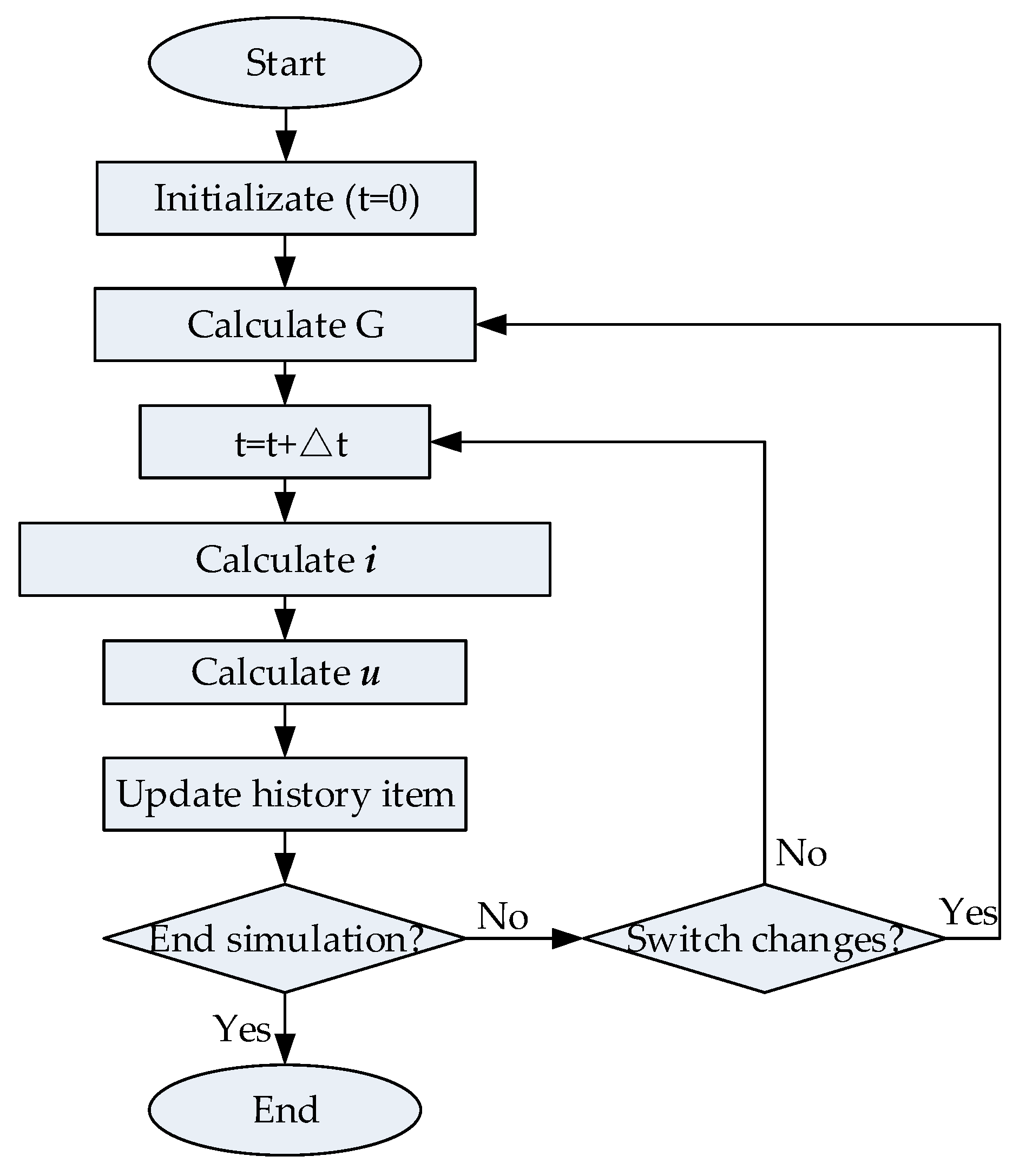
6.1. Computing Capability Test

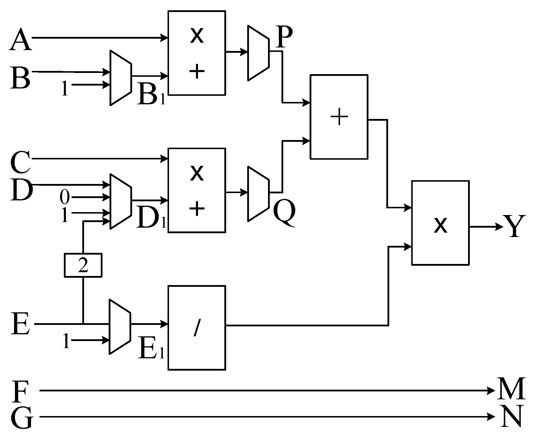
The computing capability of the solver is mainly reflected in its seriality and parallelism. The seriality is defined as the number of associated computing formulas that can be computed in one second. When performing a seriality test, the metric S s is max { f p a v } , where p a v is the average pipeline length of the formulas, which is equal to the sum of the product of the shortest pipeline length of each computing formula and its weight.
The parallelism is defined as the number of independent computing formulas that can be computed in one second. A computing component can perform m computing formulas at the same time. When performing a parallelism test, the metric S p is max { m n ( f p a v ) } . As f p a v , the metric is simplified to max { m n f } .
For the original FRTDS, the various types of computing formulas and their proportions are shown in Table 2, the shortest pipeline lengths are shown in Table 3. The average pipeline length p a v of the original FRTDS is calculated to be 14.88 p 22 . The seriality and parallelism tests were performed on the original FRTDS. The results are shown in Table 6.
An original computing component can compute two computing formulas at the same time. When performing parallelism test, the metric is max { 2 n f } , and the test results are shown in Table 7.
According to the generation method of Table 3, the new FRTDS is analyzed, and the relationship between the number of computing components that can be accommodated, the operating frequency, and the shortest pipeline length are as shown in Table 8.
The average pipeline length p a v of the new FRTDS is calculated to be 12.84 p 14 . The seriality and parallelism tests were performed on the new FRTDS. The results are shown in Table 9.
A new computing component can compute one computing formula at the same time. When performing parallelism test, the metric is max { n f } , and the test results are shown in Table 10.
As shown in Table 3 and Table 8, the shortest pipeline length of the new computing component is shorter than the original computing component; as shown in Table 6 and Table 9, the new FRTDS has a greater seriality than the original FRTDS; as shown in Table 7 and Table 10, the new FRTDS has a higher degree of parallelism than the original FRTDS.

6.2. Example Analysis

On the FRTDS-based power system real-time simulation platform, the simulation of the 110 kV substation shown in Figure 14 was performed, with a simulation step size of 50 μs. In this substation, 110 kV and 10 kV were connected by a single bus section, two inlets were connected to 110 kV bus, 12 outlets were connected to the 10 kV bus, and the No. 1 main transformer and the No. 2 main transformer were used to connect the 110 kV bus and 10 kV bus. The 12 outlets were connected to the resistive load. The system contained a total of 532 simulation nodes.
To verify the accuracy of the new FRTDS, the simulation system was also simulated with Power Systems Computer Aided Design (PSCAD).
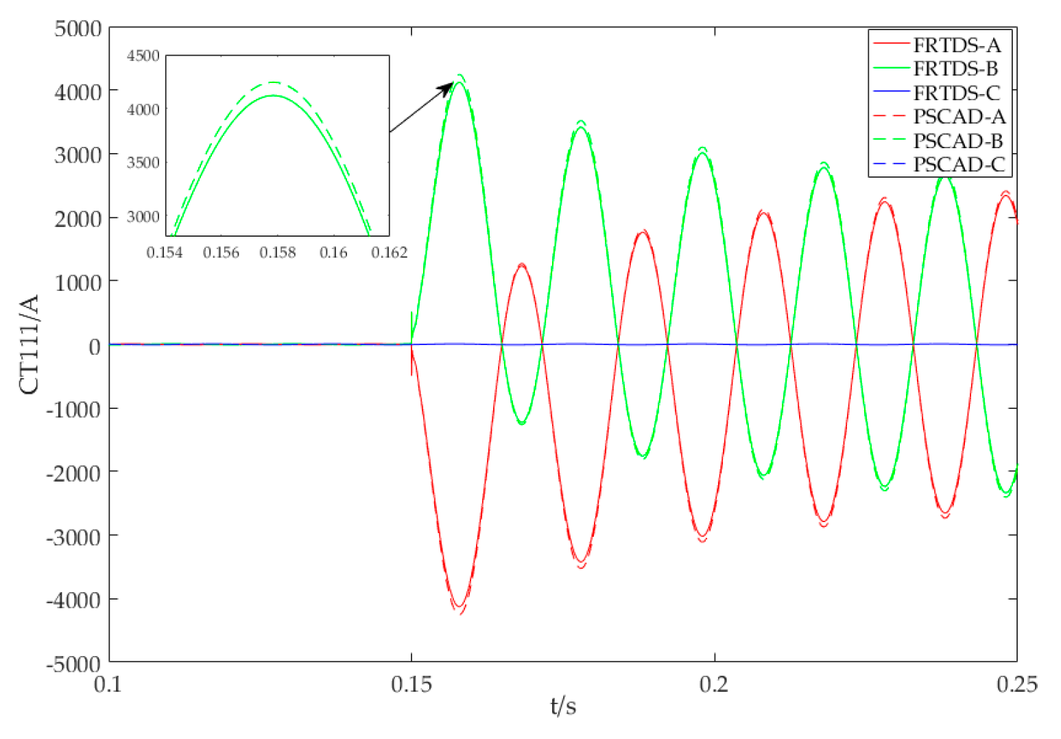
After the simulation started, at time-point t = 0.15 s, the A and B phase-to-phase short-circuit faults were set at 110 kV I bus, the voltage waveform of the fault point is shown in Figure 15 and the current waveform of 111-input line is shown in Figure 16.
Figure 15 shows after the two-phase fault occurs, both A and B phase voltage of the fault point is reduced, with the same amplitude and phase.
Figure 16 shows that after the two-phase fault occurs the currents of fault phases increase sharply relative to the opposite phase. The non-fault phase current is much lower, as compared to the other two phases.
According to Figure 15 and Figure 16, the simulation results of FRTDS and PSCAD are consistent, which proves the accuracy of new FRTDS.
To verify the efficiency of the new FRTDS, it simulates five kinds of systems using the minimum degree method. A is the left half system, with the 10 kV bus connected to the two resistive load outlets 711, 712; B is the left half system, with the 10 kV bus connected to the four resistive load outlets 711, 712, 713, 714; C is all systems, with the two 10 kV buses connected to four resistive load outlets 711, 712, 721, 722; D for all systems, with the two 10 kV buses connected to eight resistive load outlets 711, 712, 713, 714, 721, 722, 723, 724; E is the whole system, with the two 10 kV buses connected to twelve outlets.
It was simulated with six FRTDSes of different performance—FRTDS1 (large seriality, 175MHz, 3 computing components, the original version); FRTDS2 (high parallelism, 195MHz, 4 computing components, the original version); FRTDS3 (max computing capability, 175MHz, 4 computing components, the original version); FRTDS4 (large seriality, 175MHz, 11 computing components, the new version); FRTDS5 (high parallelism, 195MHz, 12 computing components, the new version); and FRTDS6 (max computing capability, 175MHz, 12 computing components, the new version). The results are shown in Table 11.
The test proved that when the simulation scale was small, the parallelism required by the system was not high, and the actual execution time mainly depended on the seriality of the FRTDS; when the simulation scale was large, the actual execution time mainly depended on the parallelism of the FRTDS. The new FRTDS serial computing capability and parallel computing capability were greatly improved. When using the new FRTDS, the requirements for the simulation scripts were lower and it was much easier for developers to operate. With a more balanced resource usage, shorter ideal execution time and higher parallel computing capability, the new FRTDS was ideal for real-time digital simulation of power systems.

7. Conclusions

1. There are many factors affecting timing closure, including the scale of the logic combined circuit, the number of destination timing components associated with the source timing components, and the use of FPGA resources. In the actual project, it is necessary to understand the hardware implementation of the logic combined circuit, and improve the timing closure conditions appositely.
2. The number of computing components, the operating frequency, and the pipeline length are inherently related. Their optimization must consider serial computing capability and parallel computing capability. When the simulation step size is short, it is necessary to emphasize the serial computing capability. When the simulation scale is relatively large, the parallel computing capability is mainly emphasized.
3. It is necessary to configure the FRTDS function properly and balance the use of FPGA resources, including the scale setting issues and resource consumption issues in the multi-value parameter query circuit, the computing core, etc. By analyzing the implementation of multi-port read/write circuit, this paper clarifies that the LUT consumption of a computing component is proportional to the square of the number of its read and write controllers.
4. It is necessary to utilize the features of the simulation program to improve the efficiency of the real-time digital solver. In this paper, according to the features of the power system simulation program the basic computing formula is characterized by a typical computing formula subset and there are multiple uses of the same variable, and the computing components with short pipeline length and low LUT consumption are constructed.

Author Contributions

Conceptualization, B.Z. and X.J.; methodology, X.J.; software, X.J., S.T. and J.Z.; validation, X.J., S.T. and Z.J.; formal analysis, B.Z. and X.J.; investigation, X.J. and Z.J.; resources, X.J. and S.T.; data curation, S.T.; writing—original draft preparation, X.J.; writing—review and editing, B.Z. and X.J.; visualization, X.J.; supervision, B.Z.; project administration, B.Z.; and funding acquisition, B.Z.

Funding

This research was funded by the National Natural Science Foundation of China, grant number 51477114.

Conflicts of Interest

The authors declare no conflict of interest.

References

  1. Strasser, T. Real-Time Simulation Technologies for Power Real-Time Simulation Technologies for Power System Design, Testing, and Analysis. IEEE Power Energy Technol. Syst. J. 2015, 2, 63–73. [Google Scholar] [CrossRef]
  2. Tian, F.; Huang, Y.; Shi, D.; Xia, T.; Qiu, W.; Hu, X.; Li, Y.; Tang, L.; Zhou, X. Developing Trend of Power System Simulation and Analysis Technology. Proc. CSEE 2014, 34, 2151–2163. [Google Scholar] [CrossRef]
  3. Xu, J.; Chen, Y. Transient Stability Parallel Simulation Based on Improved Communication Algorithm. Proc. CSEE 2006, 26, 12–18. [Google Scholar] [CrossRef]
  4. Chen, L.; Chen, Y.; Xu, Y.; Mei, S. Feasibility Study of Electromagnetic Transient Simulation Based on GPU. Power Syst. Prot. Control 2013, 41, 107–112. [Google Scholar] [CrossRef]
  5. Xu, Y.; Chen, Y.; Chen, L.; Ren, Z. Electromagnetic transient fast simulation method of PWM converter based on averaging theory. Autom. Electr. Power Syst. 2014, 38, 43–48. [Google Scholar] [CrossRef]
  6. Debnath, J.; Fung, W.; Gole, A.; Filizadeh, S. Simulation of large-scale electrical power networks on graphics processing units. Proc. IEEE Electr. Power Energy Conf. 2011, 199–204. [Google Scholar] [CrossRef]
  7. Wang, X.; Zhang, B.; Chen, M. Multi-Rate Real-Time Simulation Method Based on RTDS and FPGA Co-Simulation Platform. Autom. Electr. Power Syst. 2016, 40, 144–150. [Google Scholar] [CrossRef]
  8. Matar, M.; Iravani, R. Massively parallel implementation of AC machine models for FPGA-based real-time simulation of electromagnetic transients. IEEE Trans. Power Deliv. 2011, 26, 830–840. [Google Scholar] [CrossRef]
  9. Liu, J.; Dinavahi, V. A real-time nonlinear hysteretic power transformer transient model on FPGA. IEEE Trans. Ind. Electron. 2014, 61, 3587–3597. [Google Scholar] [CrossRef]
  10. Chen, Y.; Dinavahi, V. FPGA-based real-time EMTP. IEEE Trans. Power Deliv. 2009, 24, 892–902. [Google Scholar] [CrossRef]
  11. Wang, C.; Ding, C.; Li, P.; Wang, Z.; Lin, D.; Du, F. Transient real-time simulation of photovoltaic power generation system based on FPGA. Autom. Electr. Power Syst. 2015, 39, 13–20. [Google Scholar] [CrossRef]
  12. Zhang, B.; Fu, S.; Jin, Z.; Hu, R. A Novel FPGA-Based Real-Time Simulator for Micro-Grids. Energies 2017, 10, 1239. [Google Scholar] [CrossRef] [Green Version]
  13. Zhang, B.; Wu, Y.; Jin, Z.; Wang, Y. A Real-Time Digital Solver for Smart Substation Based on Orders. Energies 2017, 10, 1795. [Google Scholar] [CrossRef] [Green Version]
  14. Zhang, B.; Hu, R.; Tu, S.; Zhang, J.; Jin, X.; Guan, Y.; Zhu, J. Modeling of Power System Simulation Based on FRTDS. Energies 2018, 11, 2749. [Google Scholar] [CrossRef] [Green Version]
  15. Zhang, B.; Zhao, D.; Jin, Z.; Wu, Y. Multivalued Coefficient Prestorage and Block Parallel Method for Real-Time Simulation of Microgrid on FRTDS. Energies 2017, 10, 1248. [Google Scholar] [CrossRef] [Green Version]
  16. Zeng, J.; Zhang, C.; Fu, S.; Zhang, B. A multi-rate real-time simulator based on FPGA and order stream. Proc. CSU-EPSA 2017, 29, 72–77. [Google Scholar] [CrossRef]
Figure 1. Power system electromagnetic simulation process based on the node analysis method.
Energies 12 04666 g001
Figure 2. Original computing component.
Energies 12 04666 g002
Figure 3. Directed acyclic graphs (DAG) diagram.
Energies 12 04666 g003
Figure 4. Magnetic coil current and flux linkage curve.
Energies 12 04666 g004
Figure 5. Indirect addressing circuit.
Energies 12 04666 g005
Figure 6. Time coordination.
Energies 12 04666 g006
Figure 7. Information flow of multi-port read/write circuit.
Energies 12 04666 g007
Figure 8. Gating Look-Up-Table (LUT).
Energies 12 04666 g008
Figure 9. Simultaneous elimination of the interval nodes.
Energies 12 04666 g009
Figure 10. Decomposition of the back-substitution formula.
Energies 12 04666 g010
Figure 11. Data communication of original computing components.
Energies 12 04666 g011
Figure 12. New computing core.
Energies 12 04666 g012
Figure 13. New computing component.
Energies 12 04666 g013
Figure 14. 110 kV substation system.
Energies 12 04666 g014
Figure 15. Voltage waveform of the fault point.
Energies 12 04666 g015
Figure 16. Current waveform of the 111-input line.
Energies 12 04666 g016
Table 1. The Field Programmable Gate Array (FPGA) resource used by FPGA-based real-time digital solver (FRTDS).
Resource TypeTotal Number Number UsedUtilization
Look-Up-Table (LUT)433,200324,90375%
BRAM147058840%
DSP3600113131%
Table 2. The computing formula and their proportions used in the simulation program.
Types of the Computing FormulaNumber of the Computing Formula Proportion
Y = A × B / C + D 267846.07%
Y = A × B + C 145224.98%
Y = A × B / C 3906.71%
Y = A + B 3756.45%
Y = A × B + C × D 3295.66%
Y = A / B 3055.25%
Y = A × B 1282.20%
Other1562.68%
Table 3. The Shortest Pipeline Length of Computing Component.
n345
p
f/MHz
125222442
135222550
1452226/
1552328/
1652428/
1752429/
1852630/
1952857/
20534//
Note: The shortest pipeline length includes the data read and write pipeline, n is the number of computing components, p is the shortest pipeline length, and f is the operating frequency of the FRTDS.
Table 4. Pipeline length and resources of adder, multiplier, and reciprocator.
Type of ResourceAdderMultiplierReciprocator
Pipeline Length4410
Utilization of Flip Flop (FF)329114418
Utilization of LUT682136216
Utilization of DSP3914
Table 5. Selector output and pipeline length of the computing formula.
FormulaSelector OutputPipeline Length
B1D1E1PQ
Y = A + B B01 + × 12
Y = A + B + C B11 + × 12
Y = A + B + C + D BD1 + + 12
Y = A × B B01 × × 12
Y = A / E 10E × × 14
Y = A × B + C B11 × × 12
Y = A × B / E B0E × × 14
Y = A × B / E + C BEE × × 14
Y = A × B + C × D BD1 × × 12
Y = ( A × B + C ) / E B1E × × 14
Table 6. Seriality test (Original FRTDS).
n345
Ss/×103
f/MHz
1258401 77004400
1359073 79843992
1459745 8245/
1559964 8185/
16510,165 8713/
17510,781 8922/
18510,520 6838/
19510,297 5058/
2058914 //
Table 7. Parallelism test (Original FRTDS).
n345
Sp/×106
f/MHz
1257501000 1250
1358101080 1350
1458701160 /
1559301240 /
1659901320 /
17510501400 /
18511101480 /
19511701560 /
2051230//
Table 8. The shortest pipeline length of new computing component.
n111213
p
f/MHz
125141620
135141730
1451418/
1551520/
1651620/
1751621/
1851828/
1952030/
20524//
Note: The shortest pipeline length includes the data read and write pipeline, n is the number of computing components, p is the shortest pipeline length, and f is the operating frequency of the FRTDS.
Table 9. Seriality test (New FRTDS).
n111213
Ss/×103
f/MHz
125973585186815
13510,51486594907
14511,2938783/
15511,2678450/
16511,2448995/
17511,9269086/
18511,2067204/
19510,6317087 /
2059313//
Table 10. Parallelism test (New FRTDS).
n111213
Sp/×106
f/MHz
125137515001625
135148516201755
14515951740/
15517051860/
16518151980/
17519252100/
18520352220/
19521452340 /
2052255//
Table 11. Simulation time test.
FRTDSOriginal VersionNew Version
tsim/μs
FRTDS1FRTDS2FRTDS3FRTDS4FRTDS5FRTDS6
System
A10.62 13.05 11.94 9.6011.8010.79
B16.34 14.82 15.86 14.7713.4014.34
C23.17 19.60 19.33 20.9517.7217.47
D29.94 23.64 21.97 27.0721.3719.86
E38.65 31.87 29.73 34.9428.8126.88
Where t sim is the actual execution time.

