Article

Simultaneous Design of Low-Pass Filter with Impedance Matching Transformer for SONAR Transducer Using Particle Swarm Optimization

Department of Electrical Engineering, KONKUK University, Seoul 05029, Korea
*
Author to whom correspondence should be addressed.
Energies 2019, 12(24), 4646; https://doi.org/10.3390/en12244646
Submission received: 4 November 2019 / Revised: 4 December 2019 / Accepted: 5 December 2019 / Published: 6 December 2019
(This article belongs to the Section F: Electrical Engineering)

Abstract

:
Sound navigation and ranging (SONAR) systems detect a target in the front direction by using acoustic signals. A switching-type power conversion system is used to improve power efficiency, and an impedance matching circuit is used to decrease reactive power. A low-pass filter is used to improve the quality of acoustic signals. To achieve the desired voltage level for a SONAR transducer, a transformer is connected in series with a low-pass filter. In conventional design methods, design value errors occur because the components are designed independently and later combined. Moreover, if parameters that considerably impact operating characteristics are ignored in the design process, these errors will increase. Hence, time and cost losses are incurred during refabrication because operational characteristics differ from design values. To solve this problem, this study proposes the simultaneous design of a low-pass filter and impedance matching circuit, which includes critical design parameters, utilizing the particle swarm optimization algorithm. Moreover, conventional design methods were examined, and the superiority of the proposed design method to conventional methods was verified through analyses and experiments in terms of overall impedance phase and filter blocking characteristics.

1. Introduction

The acoustic receiver/transmitter system of a sound navigation and ranging (SONAR) system comprises the following: (1) A receiver/transmitter device comprising a transmitter beam former and receiver beam former, (2) an acoustic converter device that converts electrical signals generated by the receiver/transmitter device into acoustic signals, and converts acoustic signals that echo back from the target into electrical signals, and (3) a signal processer and detector that processes the target information by extracting it from the received signals and determines whether detection has occurred.
SONAR transducers normally operate at a high frequency band ranging from tens to hundreds of kHz. To implement these high-frequency voltage sources, an inverter is used that can change direct current (DC) voltage to alternating current (AC) voltage at the desired level and frequency. The voltage produced by an inverter that uses pulse width modulation (PWM) is produced in pulse form that has the same mean value as the source sine-wave voltage. If this pulse-form voltage is connected directly to a SONAR transducer, it causes a high charging and discharging current, owing to the characteristics of the transducer that are electrically similar to those of the capacitor, which damages the SONAR transducer. Moreover, the quality of the acoustic signal is determined by the harmonic distortion of the voltage supplied to the SONAR transducer and improves as it approaches a pure sine wave. Hence, a low-pass filter is needed to change the pulse wave voltage of the inverter into a sine wave.
The SONAR transducer comprises a vibrator body with a ceramic layer and thus has large complex electrical impedance. Therefore, the SONAR transducer requires large reactive power in addition to the active power used to generate the acoustic signal. The reactive power circulates through the inverter and is not related to the generation of the acoustic signal. The inverter supplies the required large reactive power, which causes an increased conduction loss in the switching element. This loss in turn leads to an increase in heat dissipation. In terms of the wiring, the increase in power causes an increase in the volume occupied by the winding owing to an increase in the diameter of the wire. For this reason, it is useful to design an impedance matching circuit that can cancel large reactance in SONAR transducers. Therefore, the SONAR transducer power system needs to simultaneously use a low-pass filter and an impedance matching circuit.

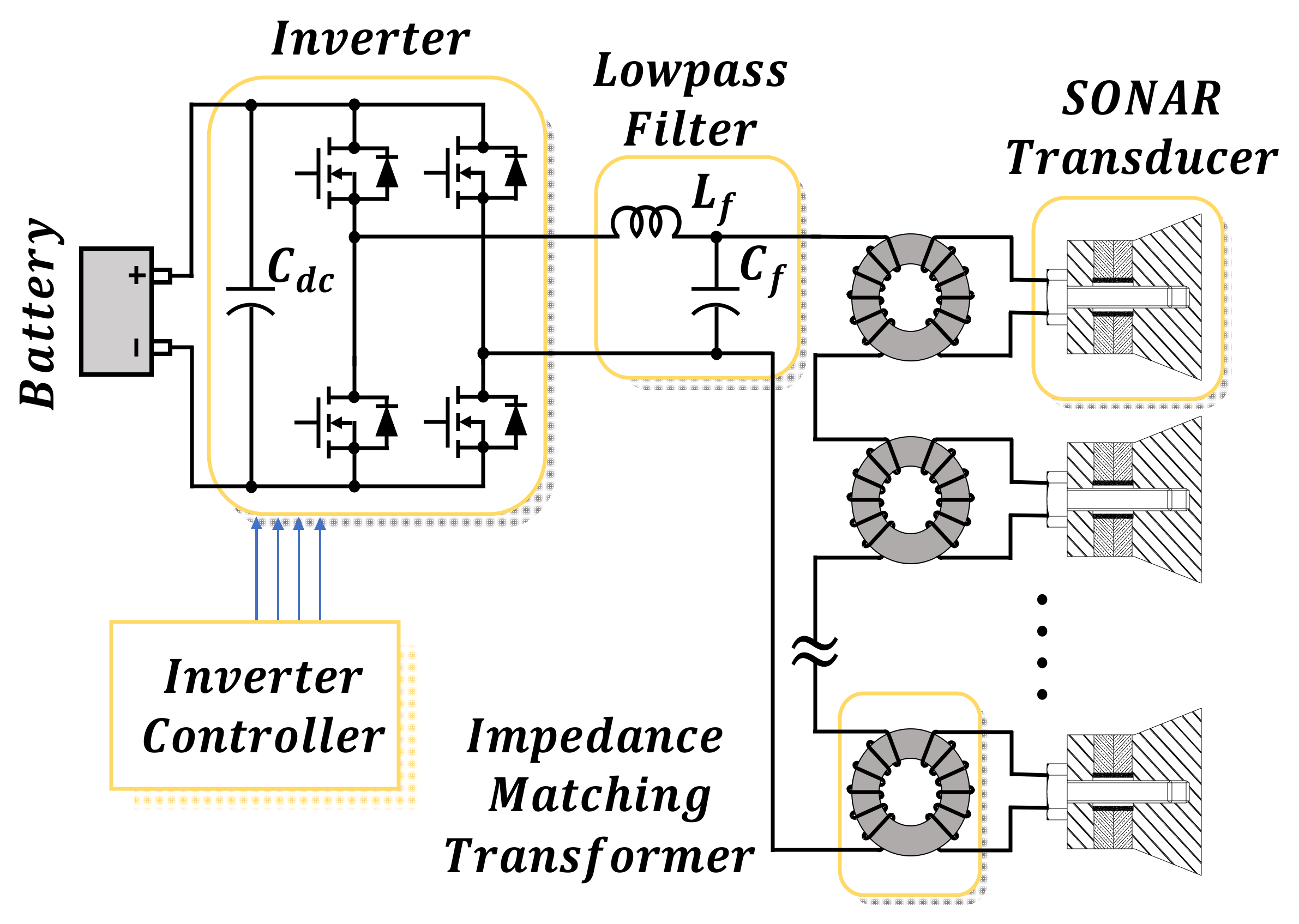
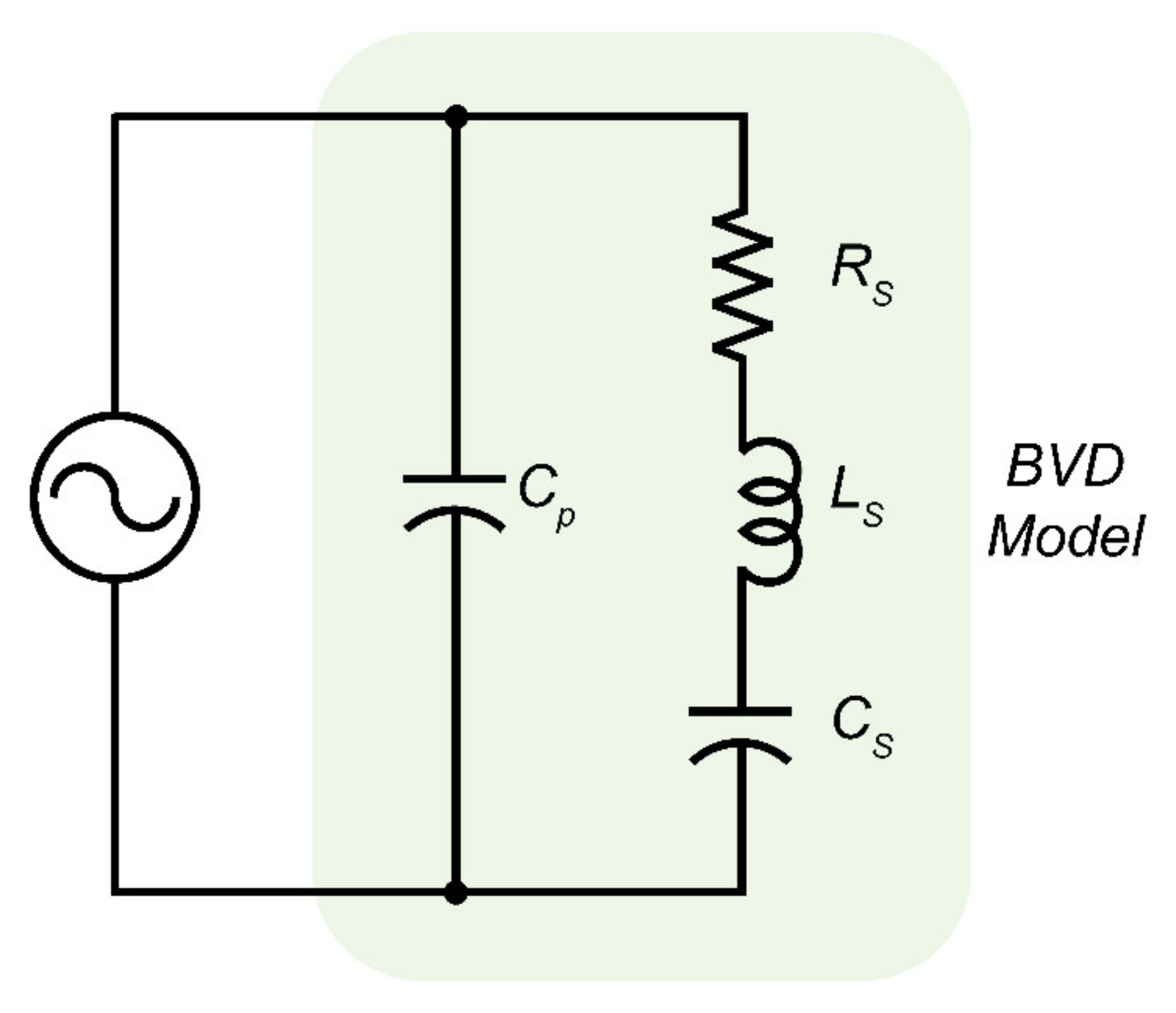
2. SONAR Transducer Power System

The system used to power the SONAR transducer comprises (1) an inverter that changes DC voltage into AC voltage, (2) a low-pass filter that converts pulse-form voltage produced by the inverter into sine-wave voltage, and (3) an impedance matching transformer to cancel reactance using magnetizing inductance and boosting the AC voltage produced by the low-pass filter. The power system used in this study comprises a structure that powers five SONAR transducers using an inverter, as shown in Figure 1. It comprises a module that connects one impedance matching transformer to each of the SONAR transducers. A total of five modules are connected in a series to create a set, which is combined with a low-pass filter to create the overall load. The overall load is then connected to the inverter to complete the SONAR transducer power system.
To verify the proposed design, some experiments using a SONAR transducer are needed; however, owing to the characteristics of SONAR transducers, changes in impedance occur because of environmental factors, such as the medium of the acoustic signal emissions and local temperature, installation method and location of the transducers, and number of units installed. For precise measurements, it is necessary to perform water tank experiments that provide an environment similar to the actual operating environment; however, these experiments may not be feasible owing to limitations in terms of their simplicity, cost, and location. Therefore, equivalent electrical models that simulate the representative impedance characteristics of a SONAR transducer are normally used as an alternative to actual SONAR transducers.
The equivalent electrical models of SONAR transducers needed to design the low-pass filter and impedance matching transformer are obtained using two methods. One method is based on the properties of the materials such as the Mason model [1] and Krimtholz, Leedom, and Matthaei model [2]. However, errors can occur owing to the use of inaccurate properties. Another is the Butterworth–Van Dyke (BVD) model [3] that is based on measurement of the impedance characteristics of a SONAR transducer in a water tank, which has an environment similar to a real operating environment. This study used the BVD model, where the resistance ( R s ), inductor ( L s ), and capacitor ( C s ) were connected in a series, and a capacitor ( C p ) was connected again in parallel. Figure 2 shows the BVD model.

3. Design of Low-pass Filter and Impedance Matching Circuit Using Conventional Methods

For impedance matching, a resistor–capacitor (RC) parallel circuit, with the same impedance characteristics as those of the SONAR transducer at a specific operating frequency, was extracted and used to design the magnetizing inductance of the transformer for eliminating reactance. In conventional methods, to simplify the design, the leakage inductance and wire resistance of the transformer are not considered. Equation (1) gives the magnetizing inductance of the transformer, L m . In Equation (1), N 1 and N 2 are the number of primary and secondary turns in the transformer, respectively, f o is the operating frequency, and C p is the capacitance of the RC parallel circuit:
L m = N 1 2 ( 2 π f o N 2 ) 2 C p .
In the low-pass filter design used in conventional methods, it is assumed that the reactance of the SONAR transducer is completely removed via impedance matching—the filter is designed assuming that the resistance of the SONAR transducer is the only load on the low-pass filter. Current methods ignore wire resistance of the filter inductor and the equivalent series resistance (ESR) of the capacitor. Equations (2) and (3) provide the chosen element values for the low-pass filter with a critically damped Butterworth response [4]. In these equations, L f is the inductance of the low-pass filter, C f is its capacitance, and R L is the load resistance. The cut-off frequency is f c o f .
L f = 2 R L f c o f ,
C f = 1 2 R L f c o f .
Table 1 presents the design values obtained using the conventional method. The following design parameters were used: N 2 / N 1 = 5 , f o = 20   kHz , C p = 283.5   nF , R L = 56.9   , and f c o f = 126.6   kHz . Figure 3 shows the results for the conventional design method, indicating differences in the characteristics between the result and reference. Because the low-pass filter and impedance matching circuit are used simultaneously, mutual influences exist whereby a design value of one side influence the design value of the other side. Therefore, when a conventional design method is used (i.e., when a low-pass filter and an impedance matching circuit are combined after being designed independently), the goal of the design will not be achieved. Furthermore, when a conventional design method is used, a significant difference is observed between the design values and actual performance because the design is obtained based on a mathematical simplification, which ignores the parameters performance for convenience of designing.
Although low-pass filter and impedance matching circuit designs are very important, the conventional design method is not useful for designing SONAR power systems. Nevertheless, studies have been carried out that only involve configuring an inverter and operating a SONAR system (e.g., an operating method using an inverter [5], reduction in total harmonic distortion of output voltage by constructing a multilevel inverter [6], and construction of a closed-loop control system by feeding back the output voltage from an open-loop control system [7]). In other words, there are few studies on low-pass filter and impedance matching circuit design methods. Therefore, this study proposes a design method using an optimization algorithm to reduce the complexity of the design method and increase its accuracy. This was achieved by reducing the errors in the actual implementation values to an effective level, compared to the design values. Furthermore, to verify the proposed method, a comparative analysis was performed to assess the conventional and proposed methods regarding the blocking characteristic of the low-pass filter through fast Fourier transform (FFT). In addition, the impedance matching characteristics of the impedance matching circuit were comparatively verified by measuring the impedance phases of the overall load model.

4. Design of Low-pass Filter and Impedance Matching Circuit Using Particle Swarm Optimization

Theoretical analysis is difficult because (1) when the low-pass filter is designed, current design methods cannot be used because the load contains higher-order terms in the transfer function, and (2) the design targets affect each other. Thus, it is necessary to create an integrated design that considers the low-pass filter, impedance matching circuit, and currently ignored components to eliminate these effects. Therefore, this study proposes a simultaneous design method that uses particle swarm optimization (PSO) to design the leakage inductance of the impedance matching transformer and wire resistance, and the wire resistance of the low-pass filter while considering parameters that were ignored in conventional methods.

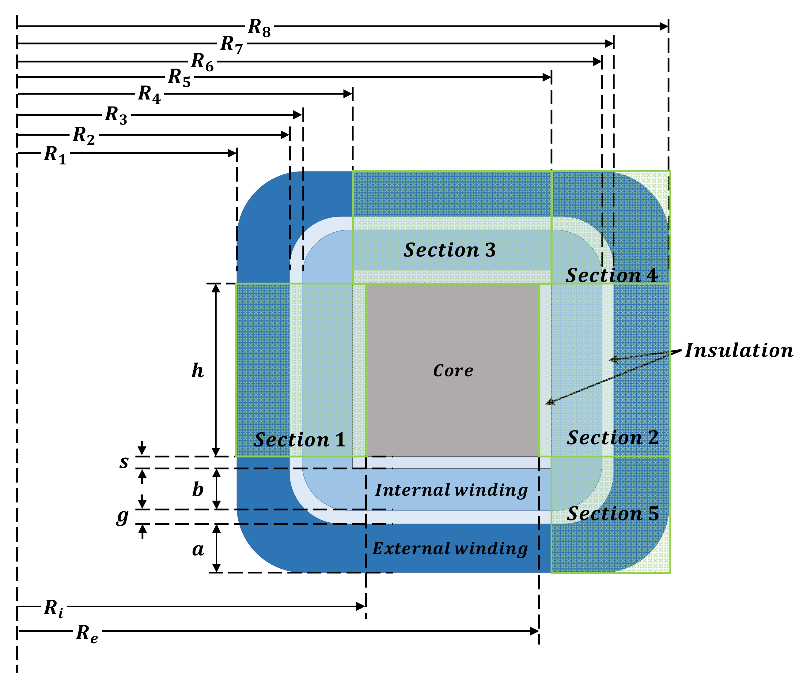
4.1. Calculating Leakage Inductance of Impedance Matching Transformer

Many studies have been devoted to calculating transformer leakage inductance. One method calculates mutual inductance and leakage inductance between transformer windings of ferromagnetic cores based on Maxwell’s equation [8]. For instance, one study used Lebedev’s approximation for calculating leakage inductance of C-type cores [9]. Some researchers have also calculated the leakage inductance of a high-frequency core-type transformer using the Biot–Savart law [10]. Another study used a differential evolution-based algorithm considering experimental results [11]. This study used a method that calculates leakage inductance using a toroidal core based on the geometrical parameters of the core and the winding [12]. Equation (4) describes leakage inductance in a transformer with a toroidal core as follows:
L l e a k = L l e a k , 1 + L l e a k , 2 + 2 L l e a k , 3 + 2 L l e a k , 4 + 2 L l e a k , 5 .
In Equation (4), L l e a k , i is the leakage inductance of the winding for each of the five sections ( i = [ 1 5 ] ) in the transformer. Section 1 and Section 2 are the internal and external vertical parts of the transformer winding, respectively. Section 3 consists of the top and bottom parts, and Section 4 and Section 5 are the corner parts, as shown in Figure 4. Equation (5) is the general equation for the leakage inductance of each section.
L l e a k , i = N 2 μ 0 2 π η i ( α i a + ϕ i g + β i b ) .
In Equation (5), N is the number of turns of the magnetic winding, μ 0 is the permeability of vacuum, and a , b ,   and   g are the external winding, internal winding, and air gap thickness, respectively. The coefficients of each section are η i ,   α i ,   ϕ i , and β i , and their values, formulas, or symbols are presented in Table 2. In Table 2, h is the height of the toroidal core, R 1 ,   R 2 ,   R 7 , and R 8 are the external and internal radii of the external winding, and R 3 ,   R 4 ,   R 5 , and R 6 are the external and internal radii of the internal winding, respectively (as shown in Figure 4).

4.2. Calculating Wire Resistance of the Impedance Matching Transformer and Filter Inductor

In calculating wire resistance, it must be considered that the AC resistance of the wire increases owing to the skin effect and proximity effect, especially at high frequencies. Many studies have been conducted on calculating the AC winding resistance of the low-pass filter and transformer, and most are based on Bennett [13] and Dowell’s one-dimensional solution [14]. This study considered the AC resistance of a high-frequency transformer using the Litz wire winding [15]. Equation (6) gives the AC resistance of the Litz wire for a unit length:
R a c = 2 N ρ π δ N o d o ( ψ 1 ( ζ ) π 2 N o β 24 ( 16 m 2 1 + 24 π 2 ) ψ 2 ( ζ ) ) ,
where
δ = ρ π f μ o μ r ζ = d o δ ψ 1 ( ζ ) = b e r ( ζ / 2 ) b e i ( ζ / 2 ) b e i ( ζ / 2 ) b e r ( ζ / 2 ) b e r 2 ( ζ / 2 ) + b e i 2 ( ζ / 2 ) ψ 2 ( ζ ) = b e r 2 ( ζ / 2 ) b e r ( ζ / 2 ) + b e i 2 ( ζ / 2 ) b e i ( ζ / 2 ) b e r 2 ( ζ / 2 ) + b e i 2 ( ζ / 2 ) .
In Equations (6) and (7), β is the packing factor, d o ,   N o , and ζ are the diameter, number of strands, and normalized value of the diameter of the strands in a conductor, respectively. The number of layers is m , δ is the skin depth, ρ and μ r are the resistivity and relative permeability of the conductor, respectively, and ψ 1 ( ζ ) and ψ 2 ( ζ ) are skin effect losses and proximity effect losses in the round conductor, respectively.

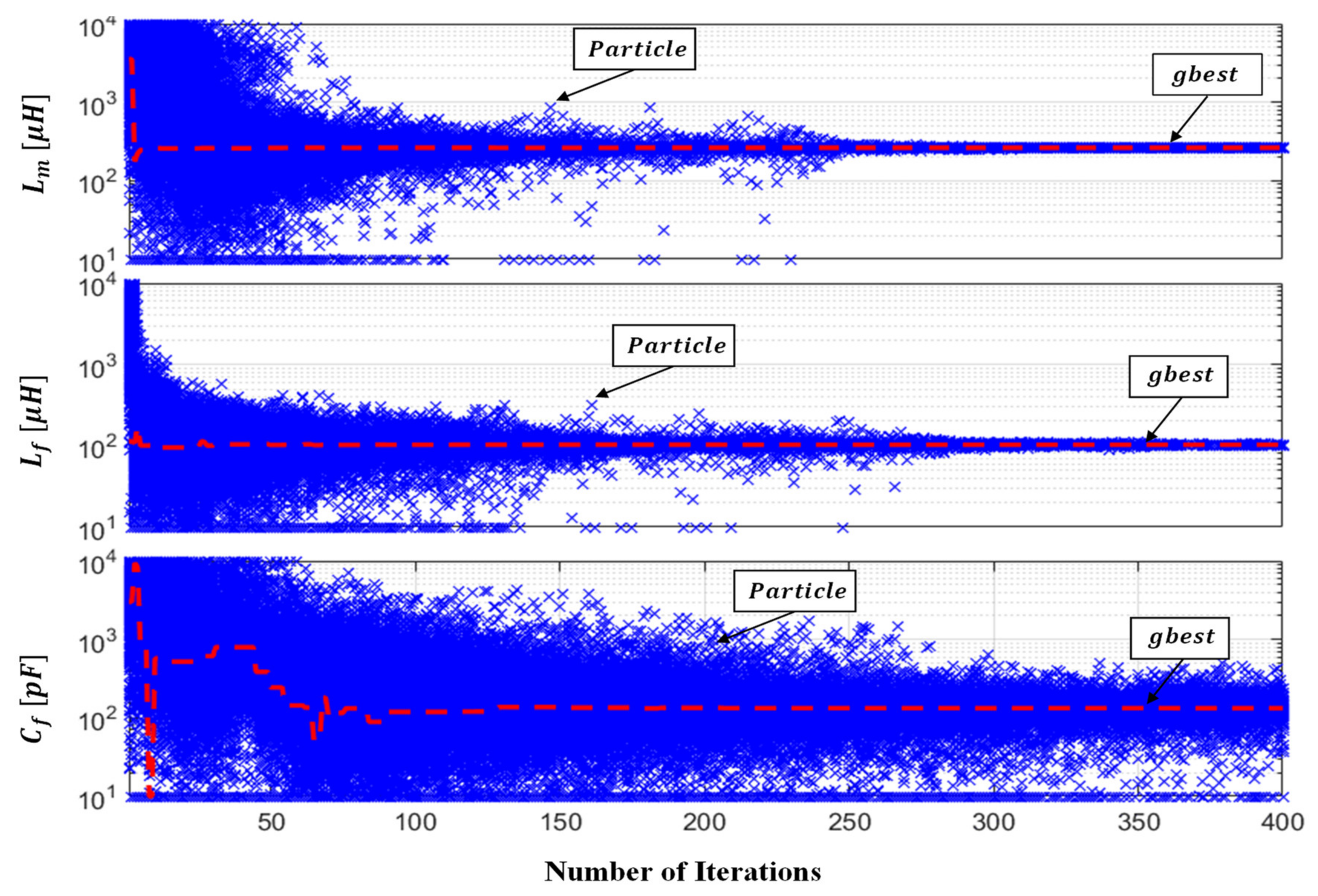
4.3. Simultaneous Design of Low-Pass Filter and Impedance Matching Circuit Using PSO
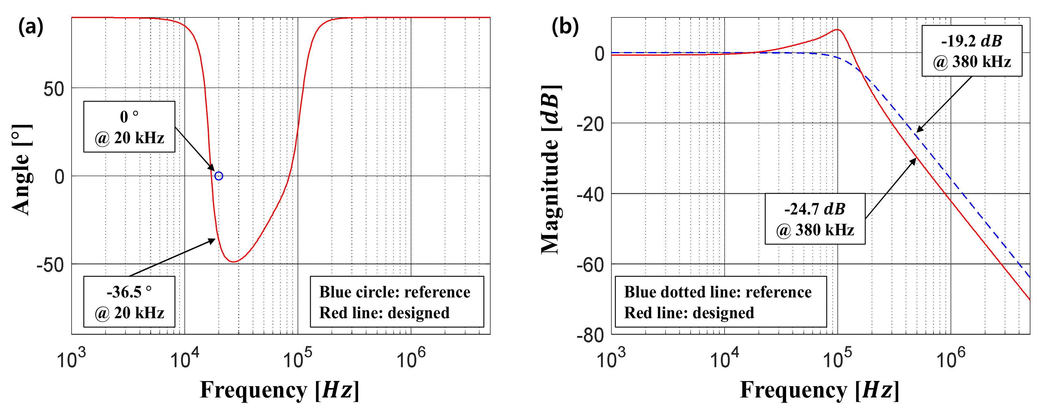
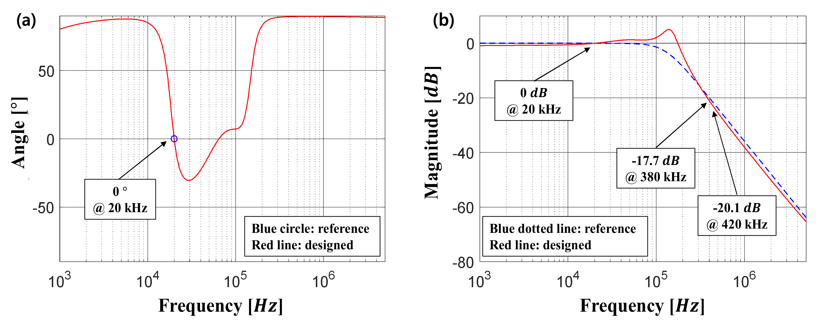
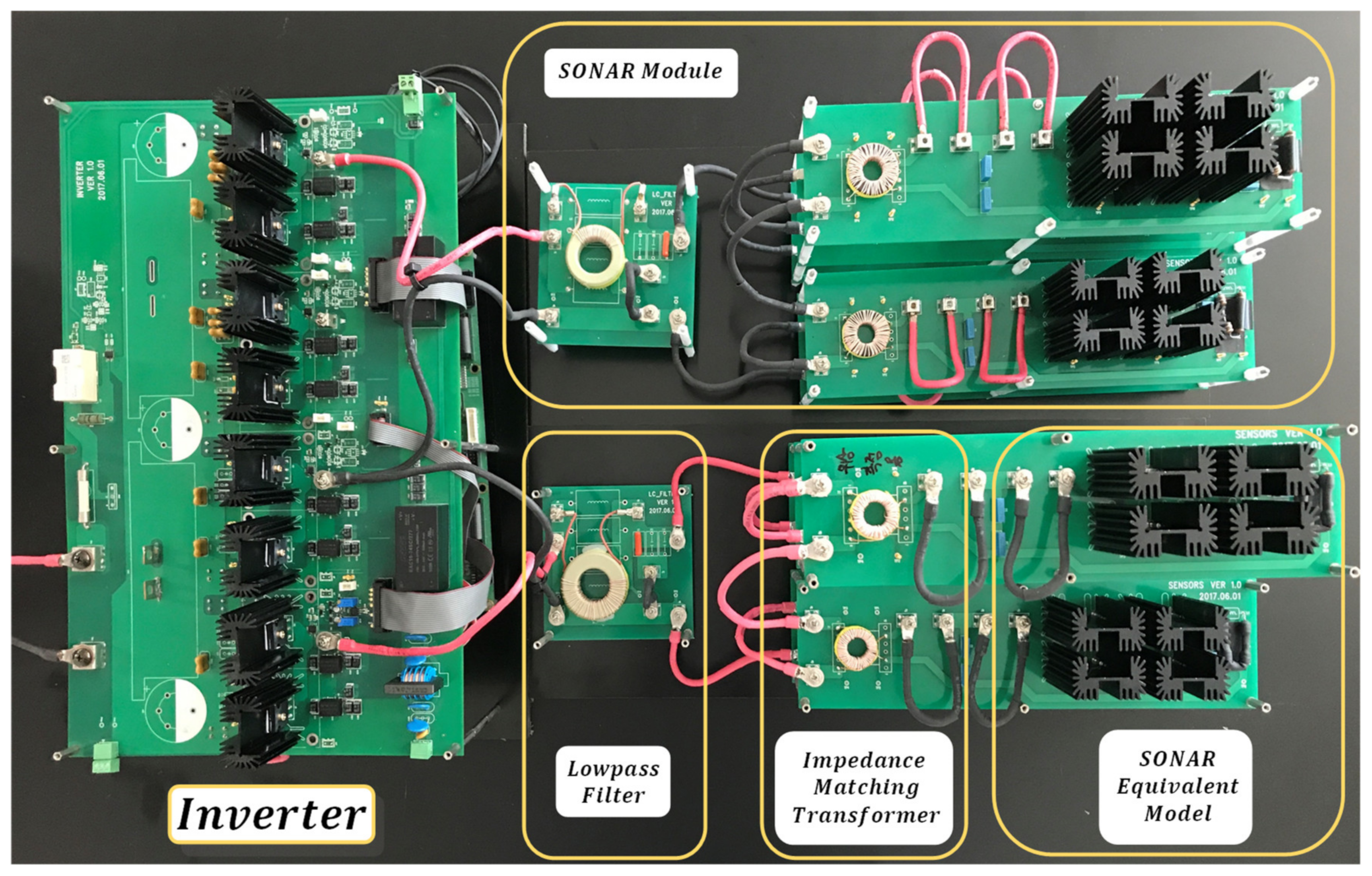
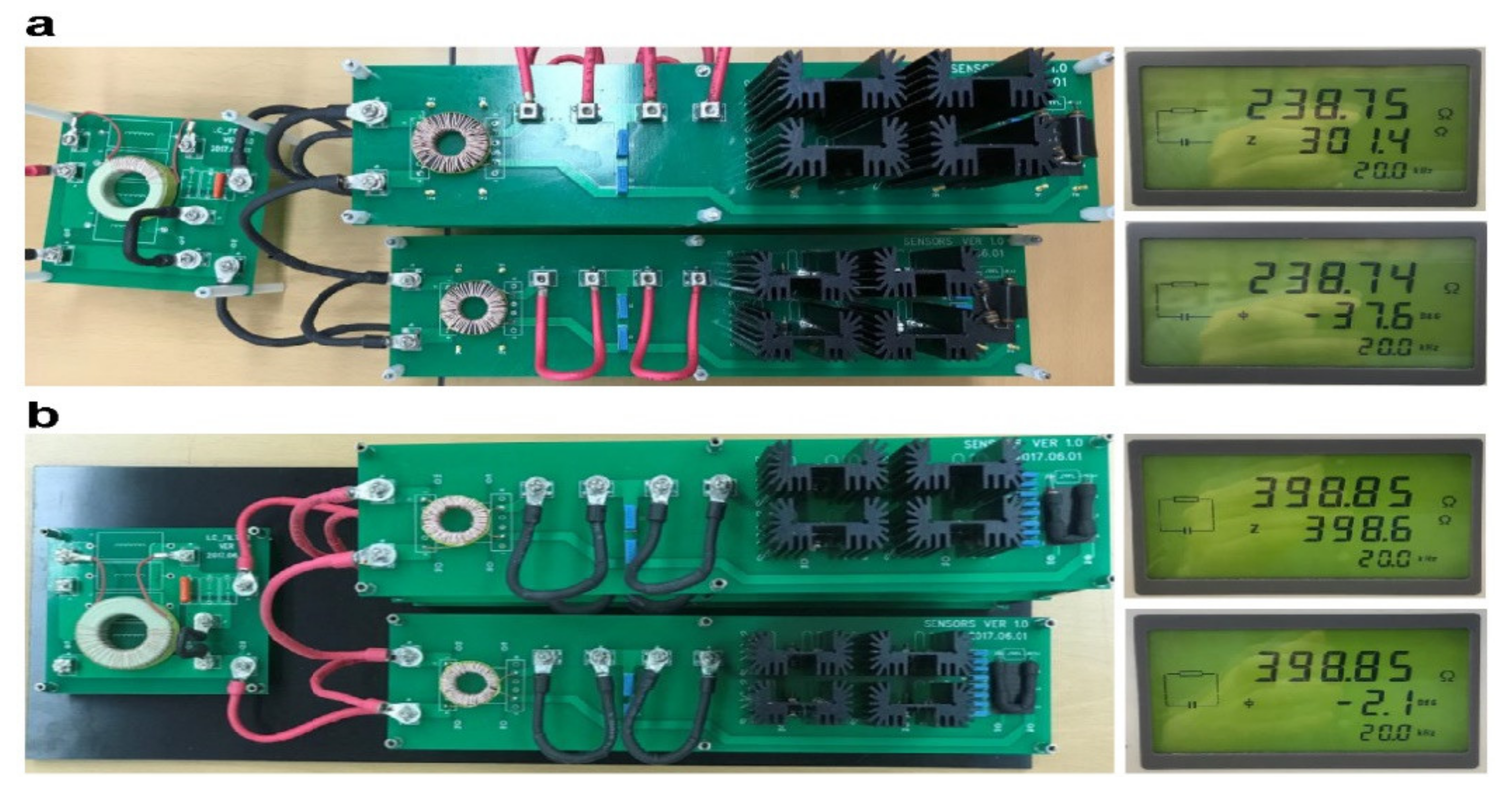
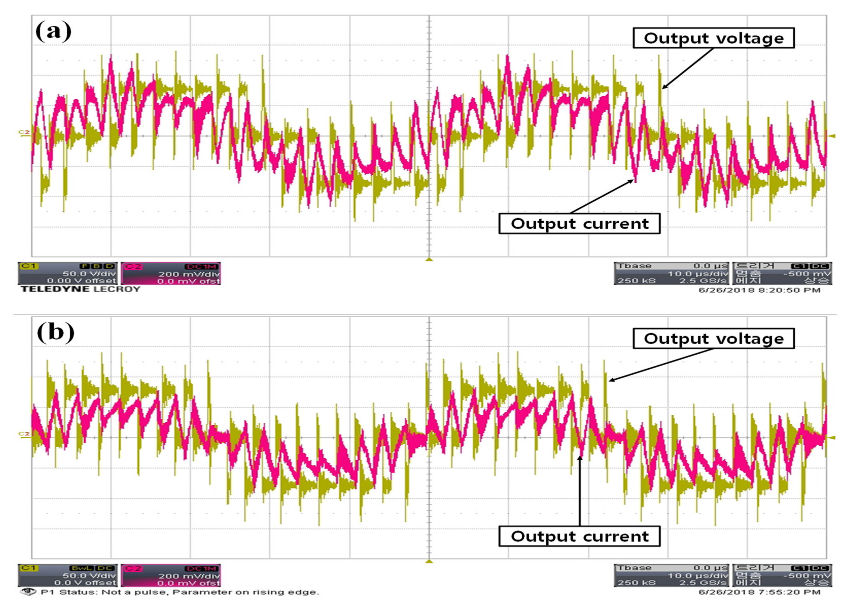
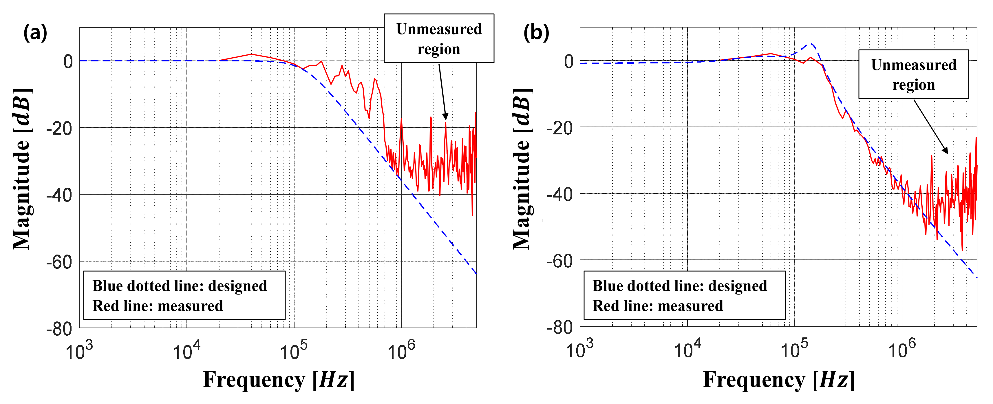
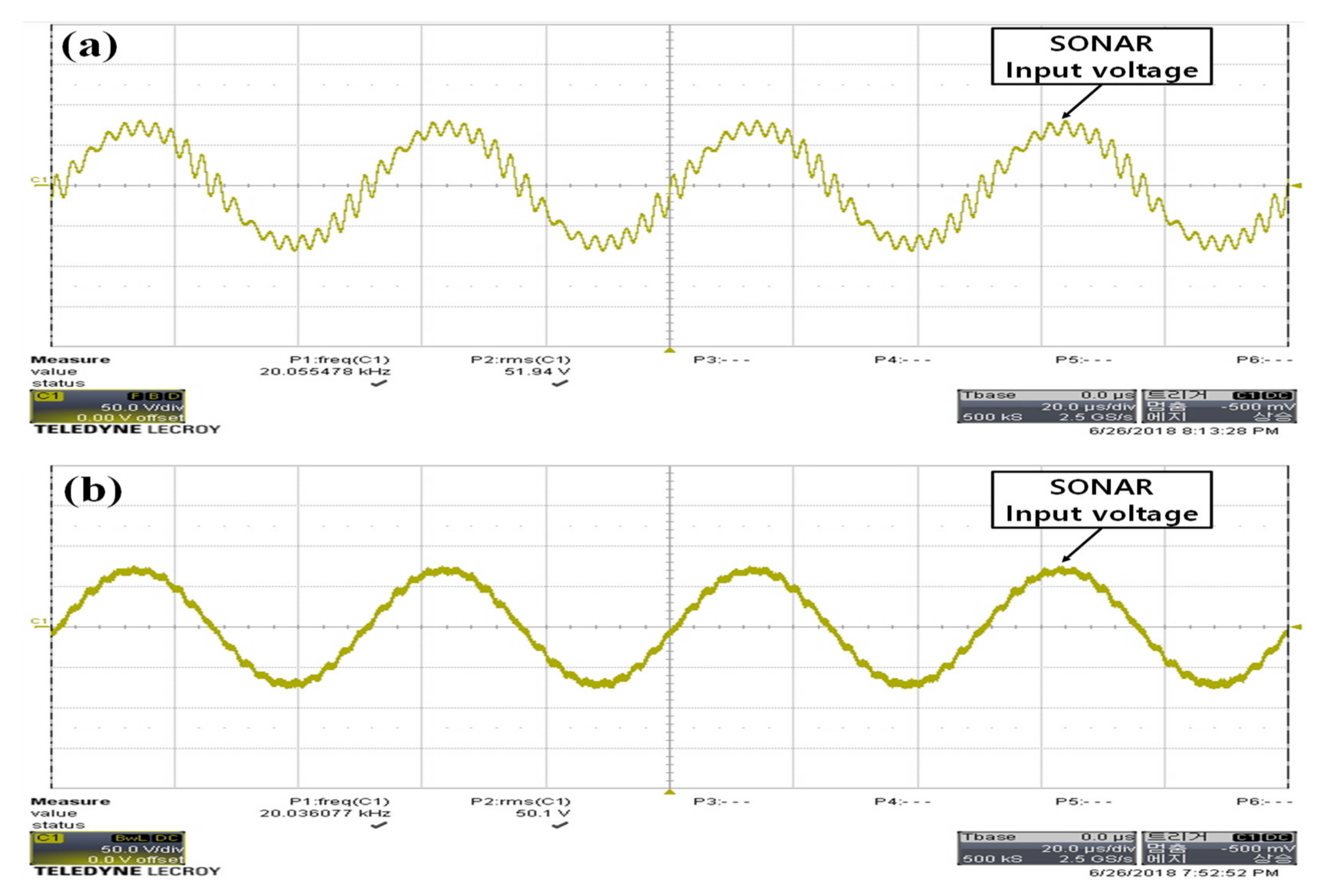
This study used the PSO algorithm [16] for simultaneously designing a low-pass filter and an impedance matching circuit considering previously omitted parameters. The PSO algorithm was developed based on swarm intelligence, such as that found in flocks of birds and schools of fish. The PSO algorithm can be used in a variety of fields. It also has very fast search performance as it does not require overlapping or mutation and transmits only the optimal information from among the optimal information of each particle [17]. However, it has a problem in that it converges on local solutions rather than optimal, global solutions when speed and direction are not accurate. In this study, a PSO algorithm with inertial weight w was used to solve the problem of convergence to local solutions [18].
A description of the proposed simultaneous design method using the PSO algorithm is provided as follows:
(1) Required input parameters: In the first step, the parameters necessary to calculate leakage inductance and wire resistance based on Equations (5) and (6) were determined.
(2) Defining default condition and initialization: Next, speed-related factors c 1 and c 2 and inertial weight w were determined. Determining inertial weight is critical because it affects the previous speed value. A large value for inertial weight means that the search area is extended, and a small inertial weight facilitates a local search. Experimental results have shown that values between 0.8 and 1.2 are most suitable in terms of convergence speed [17]. In our study, c 1 ,   c 2 and w were set to 1.49, 1.49, and 1.0, respectively. The number of particles p n u m and maximum number of iterations k m a x were also assigned in this step. p n u m and k m a x used 600 and 200, respectively. After the default condition was defined, the initial location and velocity of all particles were randomly assigned throughout the entire search area. As a result, each particle had its own design values inductance and capacitance of the low-pass filter, and magnetizing inductance of the impedance matching transformer.
(3) Calculating parameters: Because the number of turns in the transformer winding and filter inductor winding had different values to satisfy the required L f and L m for each particle, recalculation was required in every iteration that in turn affected the particle locations. As a result, the leakage inductance and wire resistance also changed according to the number of turns in every alternation. Consequently, the number of turns, leakage inductance, and wire resistance were recalculated repeatedly for each particle in the swarm during the iterative operation.
(4) Calculating the fitness of the particles: To calculate the fitness of the particles, the particles were evaluated by an objective function, given in Equation (8).
eval =   K p h Z p h e + K d b F d B e .
In Equation (8), Z p h e is the difference between the impedance phase and impedance phase reference, and F d B e is the blocking characteristic error of the low-pass filter compared with the blocking characteristic reference. Parameters K p h and K d b are weights for the phase error of the impedance and error in the blocking characteristics of the filter, respectively. Identical weights ( K p h = K d b ) were used in this study. To evaluate the objective function, a transfer function from the input voltage of the transducer to the output voltage of the inverter of the SONAR transducer was needed, which is given in Equation (9):
α 1 s + α 2 s 2 + α 3 s 3 + α 4 s 4 β 0 + β 1 s + β 2 s 2 + β 3 s 3 + β 4 s 4 + β 5 s 5 + β 6 s 6 + β 7 s 7 ,
where:
α 1 = L m N 1 N 2 ; α 2 = L m N 1 N 2 ( C s R s + C f R esr ) ; α 3 = L m N 1 N 2 C s ( L s + C f R s R esr ) ; α 4 = C s C f L s L m N 1 N 2 R esr ; β 0 = N 1 2 ( R lf + N sen R tw ) ; β 1 = N 1 2 [ L f + R lf ( C s R s + C f R esr ) + C f N sen R tw ( R esr + R lf ) + N sen ( L l + L m + C s R s R tw ) ] ; β 2 = N 1 2 [ N sen ( C s R s + C f R esr + C f R lf ) ( L l + L m ) + C s R s ( L f + C f R esr R lf ) + C s C f N sen R s ( R esr + R lf ) R tw + C f L f ( R esr + N sen R tw ) + C s L s ( R lf + N sen R tw ) ] + N 2 2 L m [ ( C p + C s ) ( R lf + N sen R tw ) ] ; β 3 = N 1 2 [ C s L s L f + C s N sen ( L l + L m ) ( L s + C f R s R esr + C f R s R lf ) + C s C f R esr ( L f R s + L s R lf ) + C s C f L s N sen R tw ( R esr + R lf ) + C f L f N sen ( L l + L m + C s R s R tw ) ] + N 2 2 L m [ ( C p + C s ) ( L f + L l N sen + C f R esr R lf + C f N sen R esr R tw + C f N sen R lf R tw ) + C p C s R s ( R lf + N sen R tw ) ] ; β 4 = N 1 2 C s C f [ L f N sen R s ( L l + L m ) + L s N sen ( L l + L m ) ( R esr + R lf ) + L s L f ( R esr + N sen R tw ) ] + N 2 2 L m [ C p C s L l N sen R s + C f L f ( C p + C s ) ( R esr + N sen R tw ) + C f N sen ( C p L l + C s L l + C p C s R s R tw ) ( R esr + R lf ) + C p C s R s ( L f + C f R esr R lf ) + C p C s L s ( R lf + N sen R tw ) ] ; β 5 = N 2 2 L m [ C f L f L l N sen ( C p + C s ) + C p C s C f N sen ( L l R s + L s R tw ) ( R esr + R lf ) + C p C s L s ( L f + L l N sen + C f R esr R lf ) + C p C s C f L f R s ( R esr + N sen R tw ) ] ; β 6 = N 2 2 C p C s C f L m [ L s L f R esr + L s L l N sen ( R esr + R lf ) + L f N sen ( L l R s + L s R tw ) ] ; β 7 = C p C s C f L s L f L l L m N 2 2 N sen .
In Equation (10), R L f ,     R e s r ,   L f , and C f are the wire resistance of the inductor of the low-pass filter, ESR of the capacitor, inductance of the inductor, and capacitance of the capacitor, respectively. R t w ,   L ,     L m ,   N 1 , and N 2 represent the wire resistance, leakage inductance, magnetizing inductance, number of primary side turns, and number of secondary side turns of the transformer, respectively. N s e n is the number of SONAR transducers connected in a series.
By calculating the object function, each particle in the swarm had its own evaluation value for each current position. Next, the particle locations were updated.
(5) Updating optimal location: In this step, if the current location was better than the old p b e s t , then p b e s t was replaced by the current location. Next, the best value between the previous g b e s t and current p b e s t was chosen as the new g b e s t . After updating, if the number of iterations exceeded the maximum number of iterations k m a x , the design procedure was ended. If not, the velocity of the particle was determined for the relative location from the best locations of each particle, p b e s t and g b e s t , using Equation (11) [18].
v i d k + 1 = w v i d k + c 1 r 1 k ( p b e s t i d k x i d k ) + c 2 r 2 k ( g b e s t d k x i d k ) ,
where v i d k , x i d k , and p b e s t i d k are the ith particle’s kth speed, location, and optimal location, respectively; g b e s t d k is the kth optimal location of the entire swarm; r 1 k and r 2 k are random values between zero and one. In this study, w = 1 and c 1 = c 2 = 1.49 were used. Next, the new locations of the particles were calculated using Equation (12). Figure 5 shows the flowchart of the proposed design method.
x i d k + 1 = x i d k + v i d k + 1 .
Figure 6 shows the movement of each particle’s location and optimal location of the entire swarm with increasing iterations. Table 3 lists the parameter values extracted using the PSO algorithm. Figure 7 shows the impedance phase and blocking characteristics of the filter that was designed using the proposed method. An operating frequency of 20 kHz and overall impedance phase of 0° was attained. With regard to the blocking characteristics of the filter, at 20 kHz, 0 dB was obtained, and magnitude damping was below the reference value of the design (the blue dotted line in Figure 3b) at 19th and 21st; these were the points where the maximum harmonics occurred in the inverter, according to the 200 kHz unipolar PWM method.

5. Experiments

To verify the proposed simultaneous design method, experiments were performed to compare the proposed method with a prevalent method using the experimental setup depicted in Figure 8. To verify the design of the impedance matching circuit, the impedance phases were measured using a FLUKE PM6304 impedance meter. In this case, the inductance will change owing to the magnitude of the applied currents. Therefore, when a measurement device that measures currents using a low voltage is used in an actual system that applies a relatively high voltage, the impedance matching characteristic can change. However, the core used in the inductor was CHANGSUNG’s CH467125, and the changes in inductance caused by the difference in electric current between the measurement device and actual system were less than 0.4% based on the inductance factor (AL value) of the core. This means the measurements obtained through the measurement device were valid. Furthermore, to verify the design of the low-pass filter, the voltage output from the inverter side and that applied to the sensor were measured. In addition, by performing an FFT analysis, the error level was comparatively analyzed with the design values from the viewpoint of harmonics reduction.
Before verifying the proposed method, the impedance of the BVD model was measured to investigate if it was implemented at a level that could be tested by replacing the actual SONAR transducer. Table 4 presents a comparison of the measured values with the design values. With respect to the magnitude of the impedance and impedance phase, the mean errors of the BVD models were 1.61% and 0.18°, respectively, confirming that it was implemented at a replaceable level. The actual values of the low-pass filter and impedance matching transformer in comparison with the design values were also elements affecting the verification experiment results; therefore, the characteristics of the low-pass filter and transformer were measured, and they are listed in Table 5 and Table 6, respectively. As observed in Table 5, the mean inductance error of the low-pass filter was 0.8%, and the mean capacitance error of the low-pass filter was 3.3%. Moreover, according to Table 6, the mean magnetizing inductance error of the impedance matching transformer was 4.8%
Figure 9 and Table 7 describe the entire load configuration, including the low-pass filter, impedance matching circuit, equivalent circuit of the SONAR transducer, and impedance measurement results. When designing using the conventional method, the impedance phase was designed based on 0° to remove all reactive power; however, during actual implementation, the error of the impedance phase was 37.6°. This error occurred because when using the conventional method, the low-pass filter and impedance matching circuit were designed independently and combined afterward. In contrast, when the proposed simultaneous design method was used, the impedance phase error was 2.1°, lower by 35.5° compared to that of the conventional design method. Therefore, impedance matching was performed at a level where readjustment of design values was unnecessary, as far as the errors between the design and implemented values were concerned. The actual measurement waveforms of the output voltage and inverter current are shown in Figure 10.
To investigate the filter blocking characteristics of the low-pass filter, the harmonics of the inverter output voltage and those of the SONAR transducer input voltage (which constituted the final load) were measured, and the reduction characteristics of the output compared with those of the input were analyzed. When designing using the conventional method, the design values of the filter blocking characteristics (Figure 11a, blue dotted line) were not satisfied. At the maximum harmonic degrees (i.e., 19th and 21st degrees), the design values of the reduction were −19.2 dB and −20.9 dB, respectively, whereas the actual reduction values were −6.4 dB and −9.8 dB, respectively. Therefore, errors of 12.8 dB and 11.1 dB occurred, respectively, compared to the design values, as indicated in Table 8. Moreover, up to the 45th harmonic degree, the mean error of the actual reduction compared to the design values was 6 dB. This error also occurred because of the conventional method of combining the low-pass filter and impedance matching circuit after designing them independently. In contrast, when designing using the simultaneous design method, the design values of the filter blocking characteristics (Figure 11b, blue dotted line) were satisfied. At the 19th and 21st degrees, which were the maximum harmonic degrees, the design values of the reduction were −20.1 dB and −22.1 dB, respectively; the actual reductions were −21.7 dB and −24 dB, respectively, confirming that errors of only 1.6 dB and 1.9 dB occurred, respectively, compared to the design values. Moreover, the mean error of the actual reduction compared to the design values up to the 45th harmonic degree was 1.3 dB. Therefore, like the impedance matching circuit, the low-pass filter did not require any readjustment owing to errors with respect to the design values. This proves the superiority of the proposed method in comparison to the conventional method. The actual measurement waveforms of the input voltage of the SONAR transducer are shown in Figure 12.

6. Conclusions

This study developed a method for simultaneously designing a low-pass filter and an impedance matching circuit, which are essential elements in systems used to power SONAR transducers. Experiments were performed to confirm the superiority of the proposed method compared to an existing method in terms of the overall impedance phase and filter blocking characteristics. When the overall impedance phase was measured to verify the design of the impedance matching circuit, the existing method showed an error of 37.6° compared to the design values, and impedance matching was not accomplished. However, the proposed method reduced the phase error to 2.1°, lower by 35.5° compared to the prevalent method. Moreover, the errors were comparatively analyzed considering the design values for each harmonic degree in terms of the output waveform of the inverter and those of the SONAR transducer to verify the blocking characteristics of the filter. In the existing method, a maximum error of 12.8 dB and mean error of 6 dB occurred, and the design values were not satisfied. However, in the proposed method, a maximum error of 1.9 dB and a mean error of 1.3 dB occurred, and the experimental values were similar to the design values.
The design method developed in our study only considered a fixed operating frequency. However, SONAR transducers tend to operate in wide-band as well as fixed operating frequencies to increase their searching performance. For wide-band operation, it is critical to apply impedance matching technology to ensure system efficiency across the frequency range.
In term of the PSO algorithm, it is important to select the initial position of the PSO algorithm, as it is related to the convergence speed and design result. This requires design engineers to have empirical knowledge on PSO algorithms; therefore, further research is needed to select the appropriate initial position.
The innovative method developed in our study which has the potential to increase accuracy and reduce refabrication costs is expected to contribute significantly as a design approach for future developments in this field.

Author Contributions

Conceptualization, J.-H.C. and H.-S.M.; methodology, J.-H.C.; software, J.-H.C.; validation, H.-S.M.; formal analysis, J.-H.C.; investigation, J.-H.C.; resources, H.-S.M.; data curation, J.-H.C.; writing—original draft preparation, J.-H.C.; writing—review and editing, H.-S.M.; visualization, J.-H.C.; supervision, H.-S.M.; project administration, H.-S.M.; funding acquisition, H.-S.M.

Funding

This research received no external funding.

Acknowledgments

This study was supported by Konkuk University in 2018.

Availability of Data and Materials

The datasets used and/or analyzed during the current study are available from the corresponding author on reasonable request.

Conflicts of Interest

The authors declare no conflict of interest.

References

  1. Mason, W.P. Electromechnical Transducers and Wave Filters; D. Van Nostrand Co.: New York, NY, USA, 1948. [Google Scholar]
  2. Krimholtz, R.; Leedom, D.A.; Matthaei, G.L. New equivalent circuits for elementary piezoelectric transducers. Electron. Lett. 1970, 6, 398–399. [Google Scholar] [CrossRef]
  3. Domarkas, V.; Kazys, R.-J. Piezoelectric Transducers for Measuring Devices; Mintis: Vilnius, Lithuania, 1975. [Google Scholar]
  4. Quek, Y.B. Class-D LC Filter Design; Texas Instruments: Dallas, TX, USA, 2008. [Google Scholar]
  5. Wood, K.E.; Bush, A.L.; Lindemann, A. New Techniques in the Design of Sonar Power Amplifiers. IEEE Power Electron. Spec. Conf. 1971, 141–146. [Google Scholar] [CrossRef]
  6. Chacko, B.P.; Panchalai, V.N.; Sivakumar, N. Multilevel digital sonar power amplifier with modified unipolar spwm. Int. Conf. Adv. Comput. Commun. Inform. 2015, 121–125. [Google Scholar] [CrossRef]
  7. Panchalai, V.N.; Chacko, B.P.; Sivakumar, N. Digitally Controlled Power Amplifier for Underwater Electro Acoustic Transducer. Int. Conf. Signal Process. Integr. Netw. 2016, 306–311. [Google Scholar] [CrossRef]
  8. Hurley, W.G. Calculation of leakage inductance in transformer windings. IEEE Trans. Power Elec. 1994, 9, 121–126. [Google Scholar] [CrossRef]
  9. Doebbelin, R.; Benecke, M.; Lindemann, A. Calculation of leakage inductance of core-type transformers for power electronic circuits. Int. Power Electron. Motion Control Conf. 2008, 1280–1286. [Google Scholar] [CrossRef]
  10. Duppalli, V.S.; Sudhoff, S. Computationally efficient leakage inductance calculation for a high-frequency core-type transformer. IEEE Electr. Ship Technol. Symp. 2017, 635–642. [Google Scholar] [CrossRef]
  11. Tria Lew, A.R.; Zhang, D.; Fletcher, J.E. High-frequency planar transformer parameter estimation. IEEE Trans. Mag. 2015, 51. [Google Scholar] [CrossRef]
  12. Hernández, I.; de León, F.; Gómez, P. Design formulas for the leakage inductance of toroidal distribution transformers. IEEE Trans. Power Deliv. 2011, 26, 2197–2204. [Google Scholar] [CrossRef]
  13. Bennett, E.; Larson, S.C. Effective resistance to alternating currents of multilayer windings. Electr. Eng. 1940, 59, 1010–1016. [Google Scholar] [CrossRef]
  14. Dowell, P.L. Effects of eddy currents in transformer windings. Proc. IEE 1966, 113, 1387–1394. [Google Scholar] [CrossRef]
  15. Tourkhani, F.; Viarouge, P. Accurate analytical model of winding losses in round Litz wire windings. IEEE Trans. Mag. 2001, 37, 538–543. [Google Scholar] [CrossRef]
  16. Kennedy, J.; Eberhart, R. Particle swarm optimization. In Proceedings of the International Conference on Neural Networks, Perth, Australia, 27 November–1 December 1995; pp. 1942–1948. [Google Scholar] [CrossRef]
  17. Bai, Q. Analysis of particle swarm optimization algorithm. Comput. Inf. Sci. 2010, 3, 180–184. [Google Scholar] [CrossRef] [Green Version]
  18. Shi, Y.; Eberhart, R. A modified particle swarm optimizer. 1998 IEEE International Conference on Evolutionary Computation Proceedings, IEEE World Congress on Computational Intelligence (Cat. No.98TH8360), Anchorage, AK, USA, 4–9 May 1998; pp. 69–73. [Google Scholar] [CrossRef]
Figure 1. Sound navigation and ranging (SONAR) transducer power system diagram.
Energies 12 04646 g001
Figure 2. Butterworth–Van Dyke (BVD) model.
Energies 12 04646 g002
Figure 3. Design values for characteristics of impedance phase and filter blocking using conventional method: (a) Impedance phase characteristics and (b) filter blocking characteristics.
Energies 12 04646 g003
Figure 4. Main geometrical parameters of a toroidal transformer.
Energies 12 04646 g004
Figure 5. Flowchart showing simultaneous design of low-pass filter and impedance matching circuit using particle swarm optimization (PSO) algorithm.
Energies 12 04646 g005
Figure 6. Movement of the particle locations and optimal location of the entire swarm.
Energies 12 04646 g006
Figure 7. Characteristics of impedance phase and filter blocking determined using proposed method: (a) Impedance phase characteristics and (b) Filter blocking characteristics.
Energies 12 04646 g007
Figure 8. Experimental setup.
Energies 12 04646 g008
Figure 9. Entire load configuration and measurement of impedance characteristics: (a) Prevalent method and (b) proposed method.
Energies 12 04646 g009
Figure 10. Output voltage and current waveform of inverter: (a) Prevalent method and (b) proposed method.
Energies 12 04646 g010
Figure 11. Comparison of blocking characteristics of low-pass filter obtained using the (a) proposed method and (b) prevalent method.
Energies 12 04646 g011
Figure 12. Input voltage waveforms of sonar transducer obtained using the (a) prevalent method and (b) proposed method.
Energies 12 04646 g012
Table 1. Design parameters obtained using the conventional method.
CategoryValue
Filter inductor inductance121.39 μ H
Filter capacitor capacitance116.64 pF
Transformer magnetizing inductance263.45 μ H
Table 2. Coefficient components of the leakage inductance formula.
SectionCoefficient
η i α i ϕ i β i
1 h ( R 1 + R 2 ) 6 R 2 2 ( R 2 + R 3 ) 4 R 2 R 3 ( R 3 + R 4 ) 6 R 3 2
2 h ( R 7 + R 8 ) 6 R 7 2 ( R 2 + R 3 ) 4 R 2 R 3 ( R 5 + R 6 ) 6 R 6 2
3 R e 2 R i 2 R e R i 1 3 1 1 3
4 1 2 R 2 2 ( R 1 + R 2 ) t 1 12 ( R 2 + R 3 ) t 2 2 ( R 3 + R 4 ) t 3 12
5 1 2 R 6 2 ( R 7 + R 8 ) t 1 12 ( R 6 + R 7 ) t 2 2 ( R 5 + R 6 ) t 3 12
Table 3. Extracted parameters using PSO algorithm.
CategoryValue
Filter inductor inductance121.39 μ H
Filter inductor wire resistance547.1 m Ω
Filter capacitor capacitance116.64 pF
Transformer magnetizing inductance263.45 μ H
Transformer leakage inductance217.36 nH
Transformer wire resistance173.4 m Ω
Table 4. Comparison of impedance characteristics with BVD models.
CategoryImpedance Phase (°)
@20 kHz
Error (°)Impedance Magnitude ( Ω )
@20 kHz
Error (%)
Design value−67.94-757.03-
Model 1−68.20.26767.51.38
Model 2−68.20.26767.61.40
Model 3−68.10.16774.32.28
Model 4−680.06768.21.48
Model 5−68.10.16768.51.52
Mean value−68.10.18769.21.62
Table 5. Inductance and capacitance of low-pass filter.
CategoryInductance @20 kHzMean Error (%)Capacitance @20 kHzMean Error (%)
Conventional methodDesign value101.2   uH 0.815.6 nF 3.3
Actual value100.8   uH 15.1 nF
Proposed methodDesign value121.4   uH 116.6 pF
Actual value120.0   uH 120.0 pF
Table 6. Magnetizing inductance of impedance matching transformer
CategoryMagnetizing Inductance ( u H ) @20 kHz Error (%)
Design value263.5-
Transformer 1282.37.2
Transformer 22733.6
Transformer 3274.84.3
Transformer 4276.44.9
Transformer 5274.34.1
Mean value274.14.8
Table 7. Comparison of impedance characteristics with entire load.
CategoryImpedance Phase (°) @20 kHzError (%)Impedance Magnitude ( Ω ) @20 kHz Error (%)
Conventional
method
Design value037.6309.01.0
Actual value−37.6301.4
Proposed
method
Design value02.1403.90.7
Actual value−2.1398.6
Table 8. Comparison of harmonic characteristics of input voltage in a sonar transducer.
Harmonic DegreePrevalent MethodProposed Method
Design Value (dB)Actual Value (dB)Error
(dB)
Design Value (dB)Actual Value (dB)Error
(dB)
Fundamental0.00.20.20.00.10.1
17−17.3−116.3−17.7−19.21.5
19−19.2−6.412.8−20.1−21.71.6
21−20.9−9.811.1−22.1−241.9
23−22.4−22.90.5−23.9−25.31.4
35−29.7−34.14.4−31.7−32.81.1
37−30.7−32.31.6−32.7−34.21.5
39−31.6−38.56.9−33.7−32.80.9
41−32.5−38.86.3−34.6−36.41.8
43−33.3−36.22.9−35.4−36.71.3
45−34.1−41.17.0−36.2−36.40.2

