Thermoelectric Properties of Carbon Nanotubes


Abstract
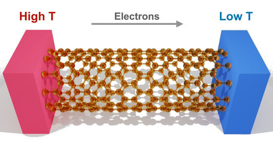
1. Introduction
2. Basic Parameters for Thermoelectric Materials
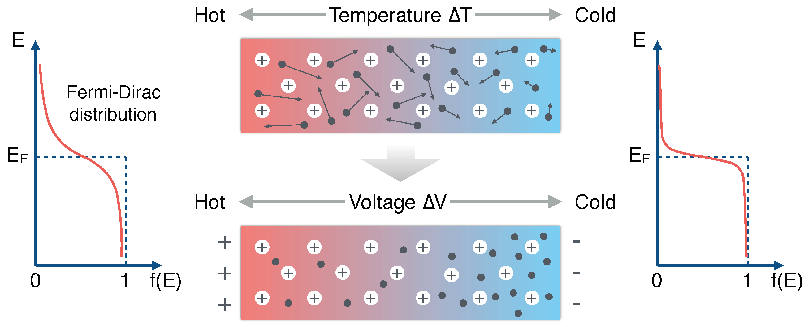
2.1. Seebeck’s Effect
2.2. Power Factor PF and Figure of Merit ZT
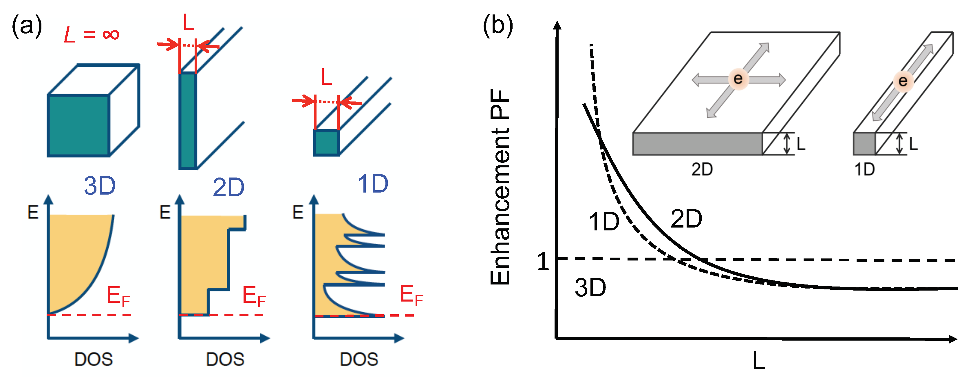
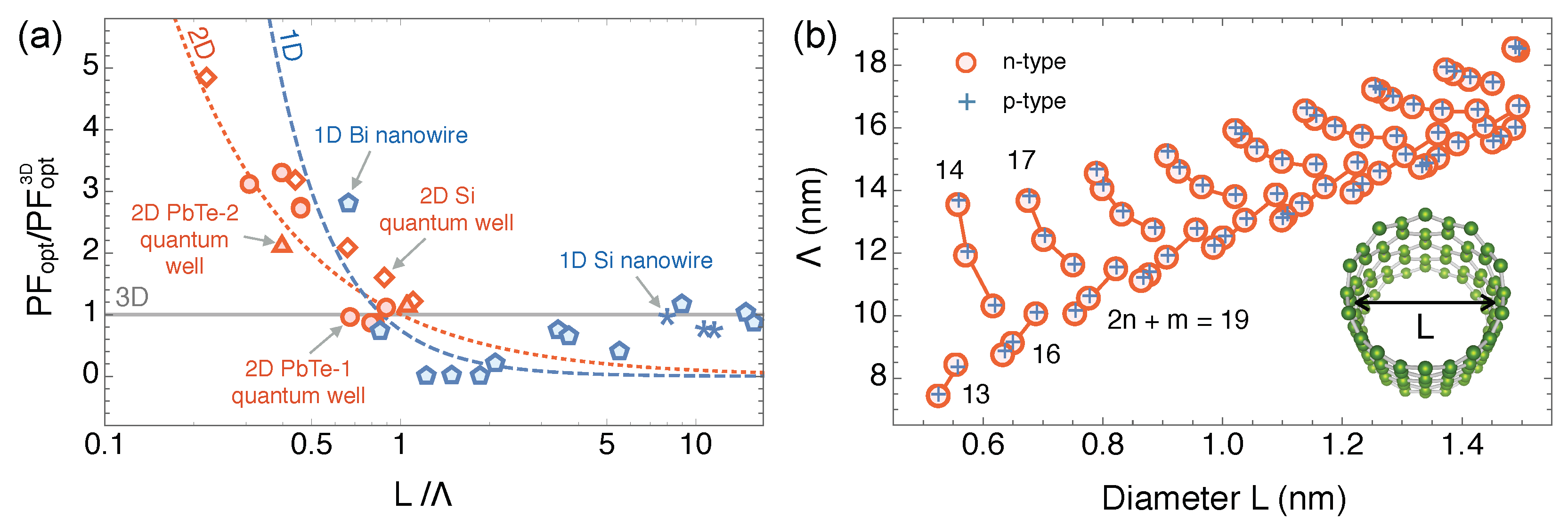
2.3. Low-Dimensional Thermoelectric Energy Conversion
3. Thermoelectric Properties of SWNTs
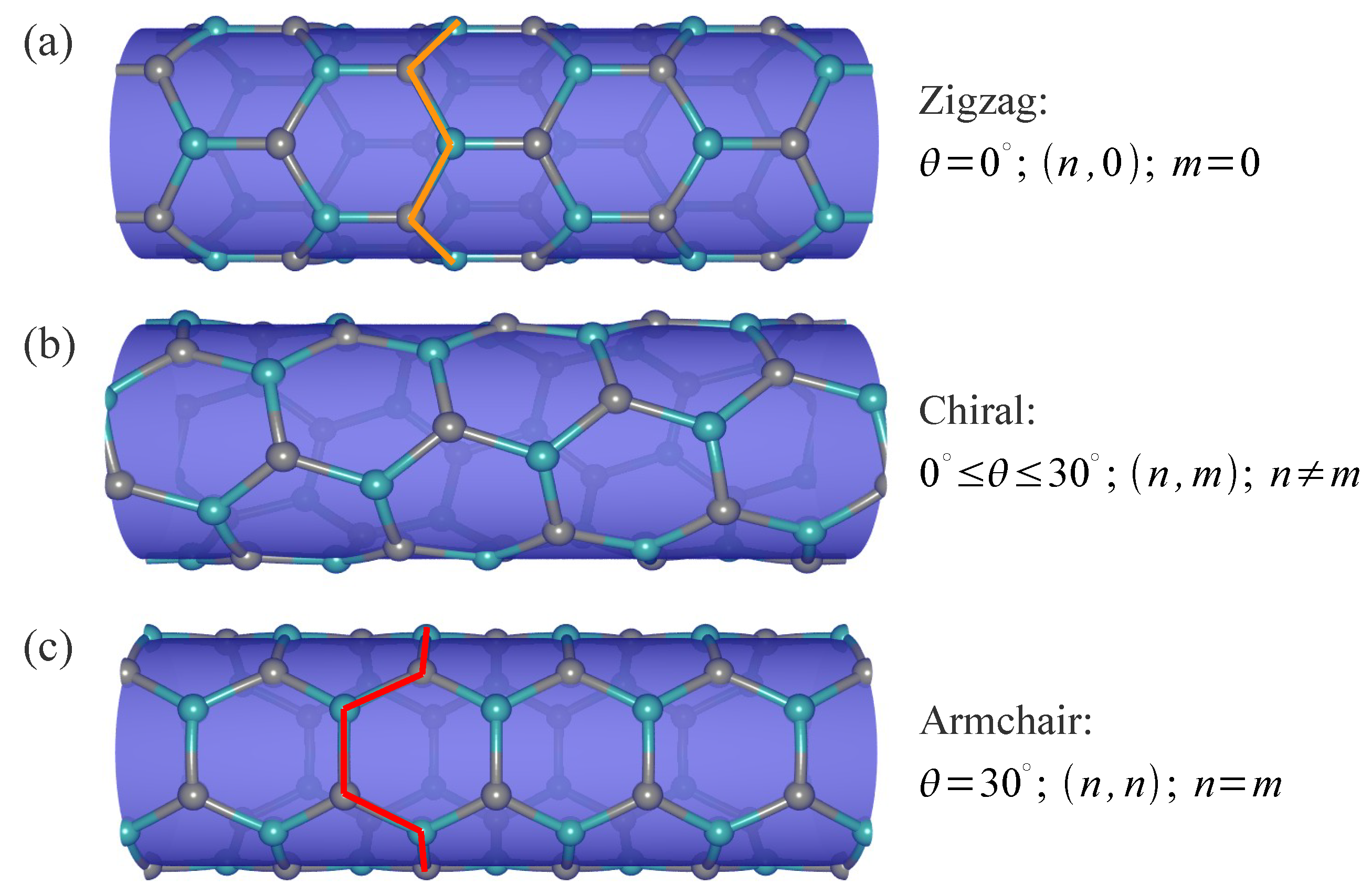
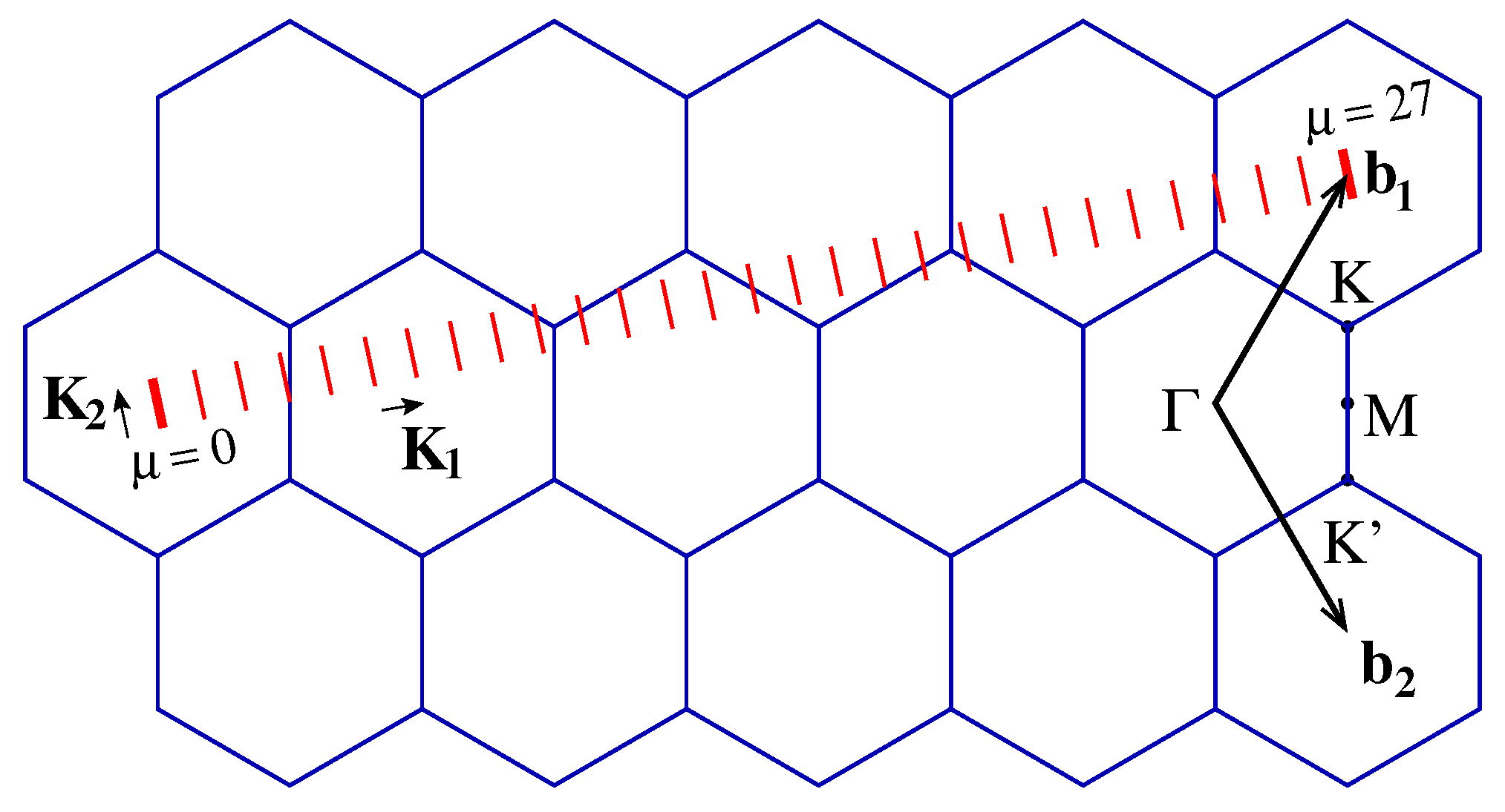
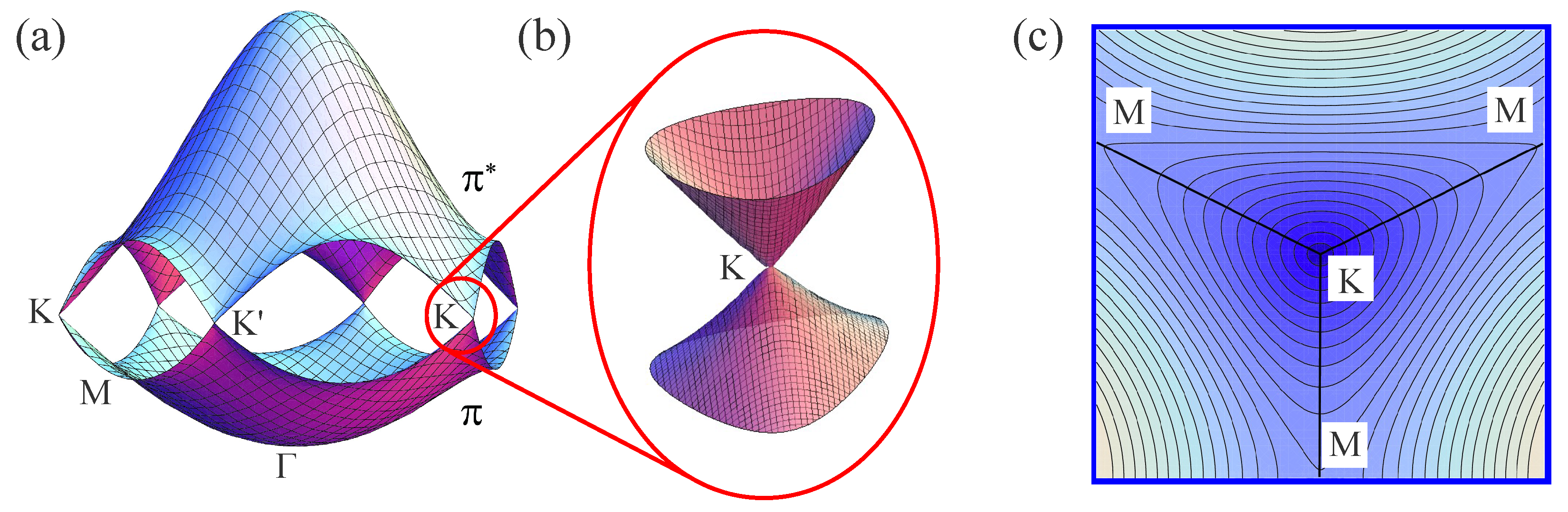
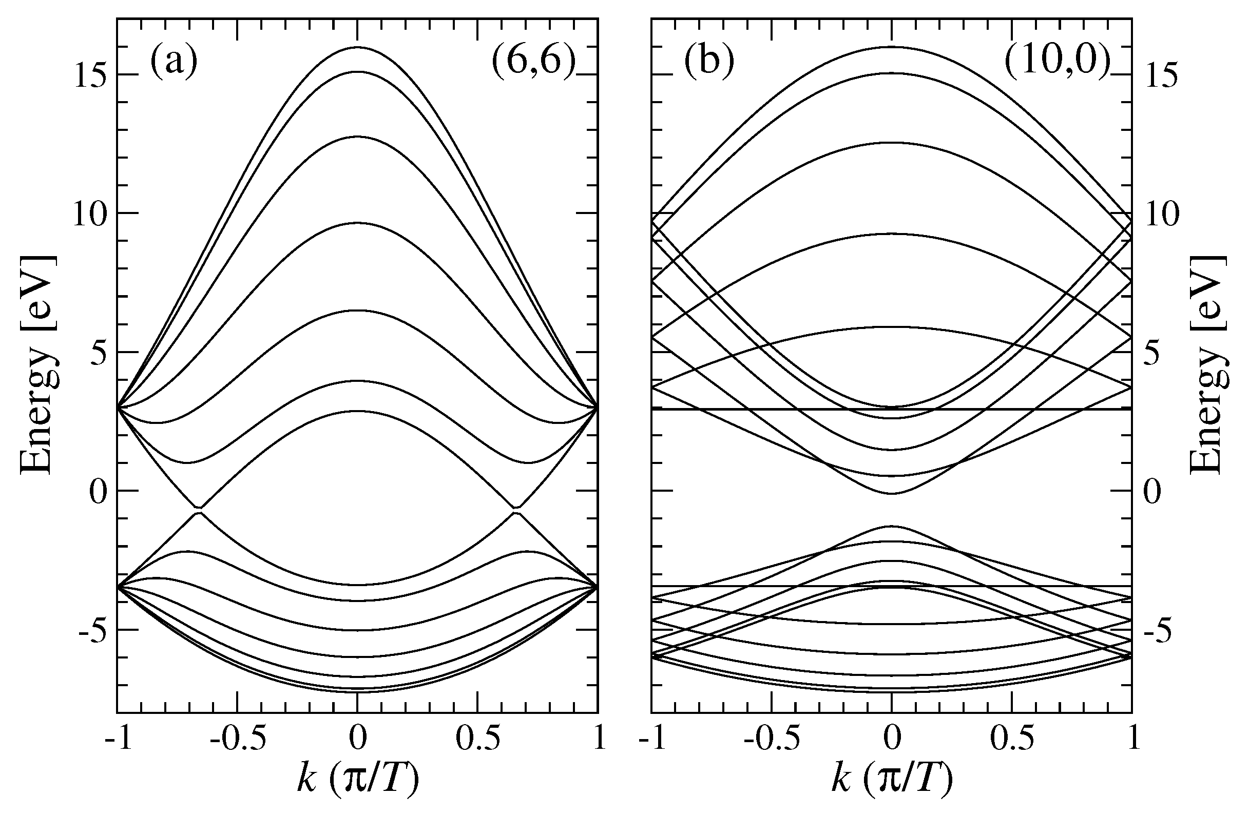
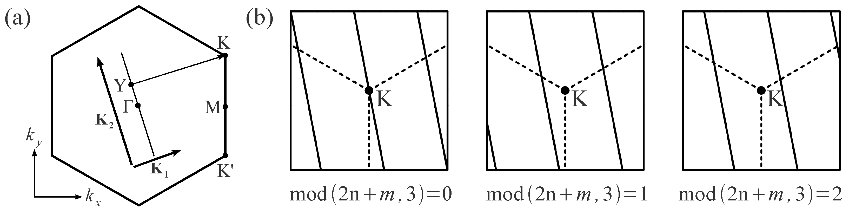
3.1. Electronic Properties of SWNTs
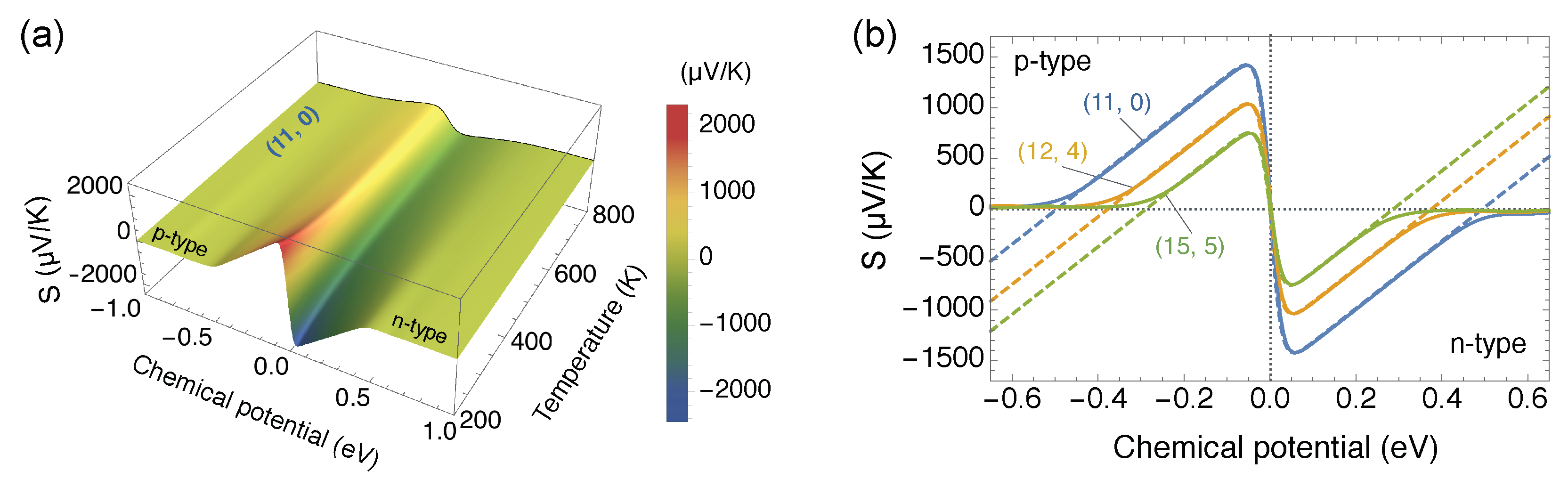
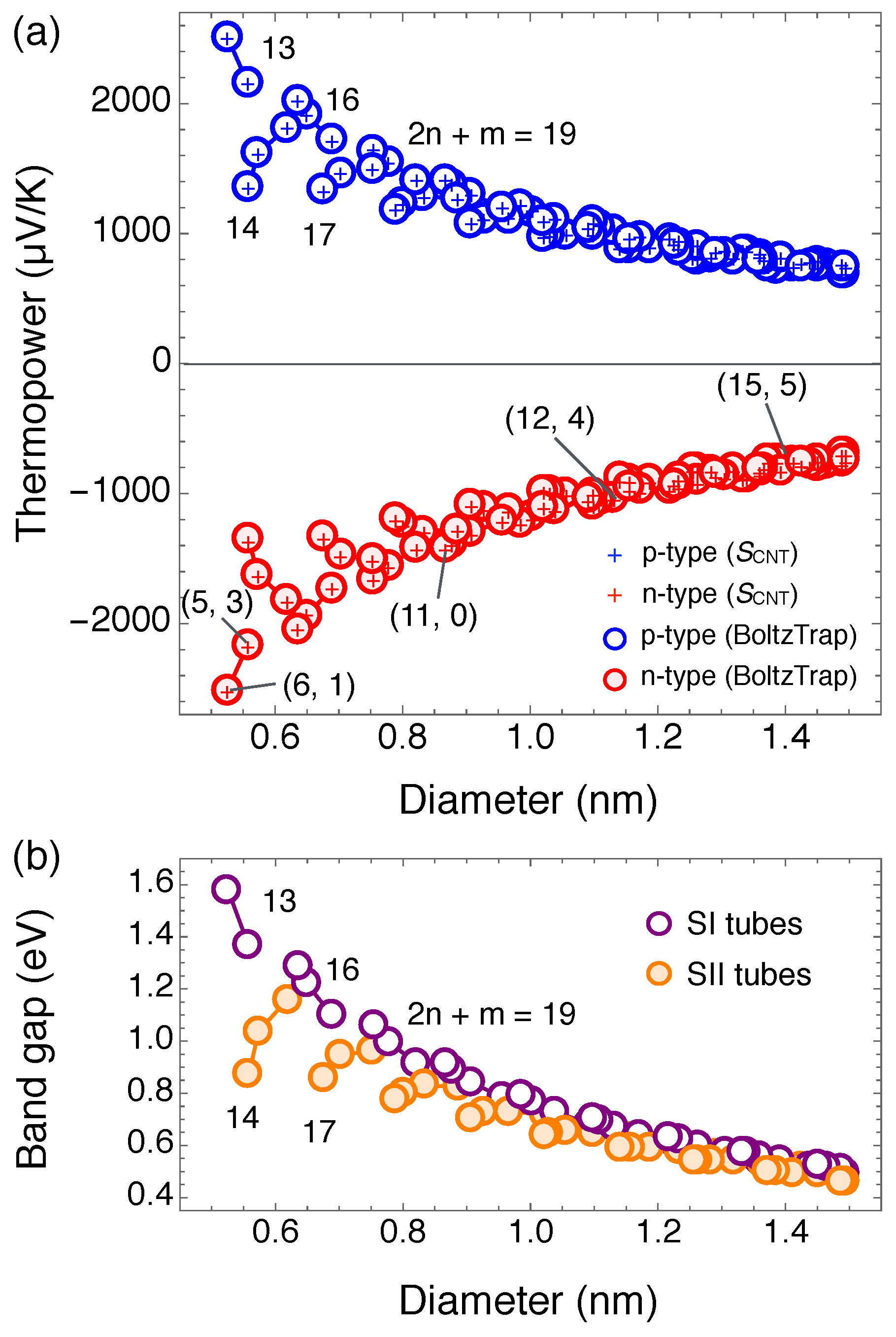
3.2. Seebeck Coefficient of SWNTs
3.3. Thermoelectric Power Factor of SWNTs
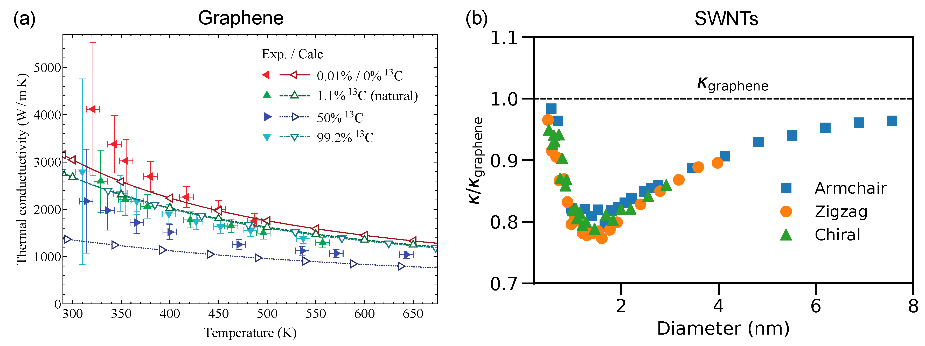
3.4. Thermal Conductivity and Figure of Merits of SWNTs
4. Strategies to Improve the TE Properties of SWNTs
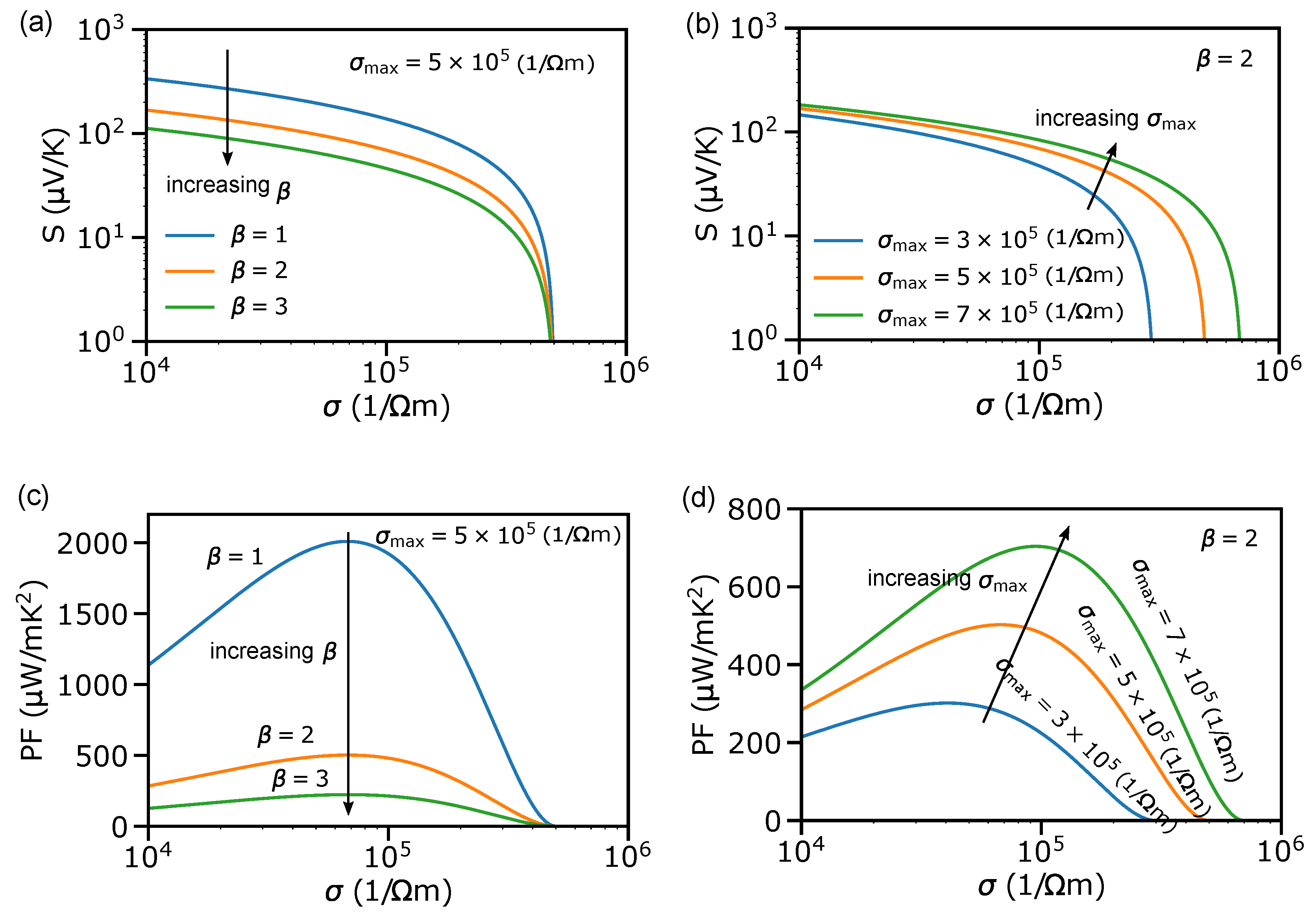
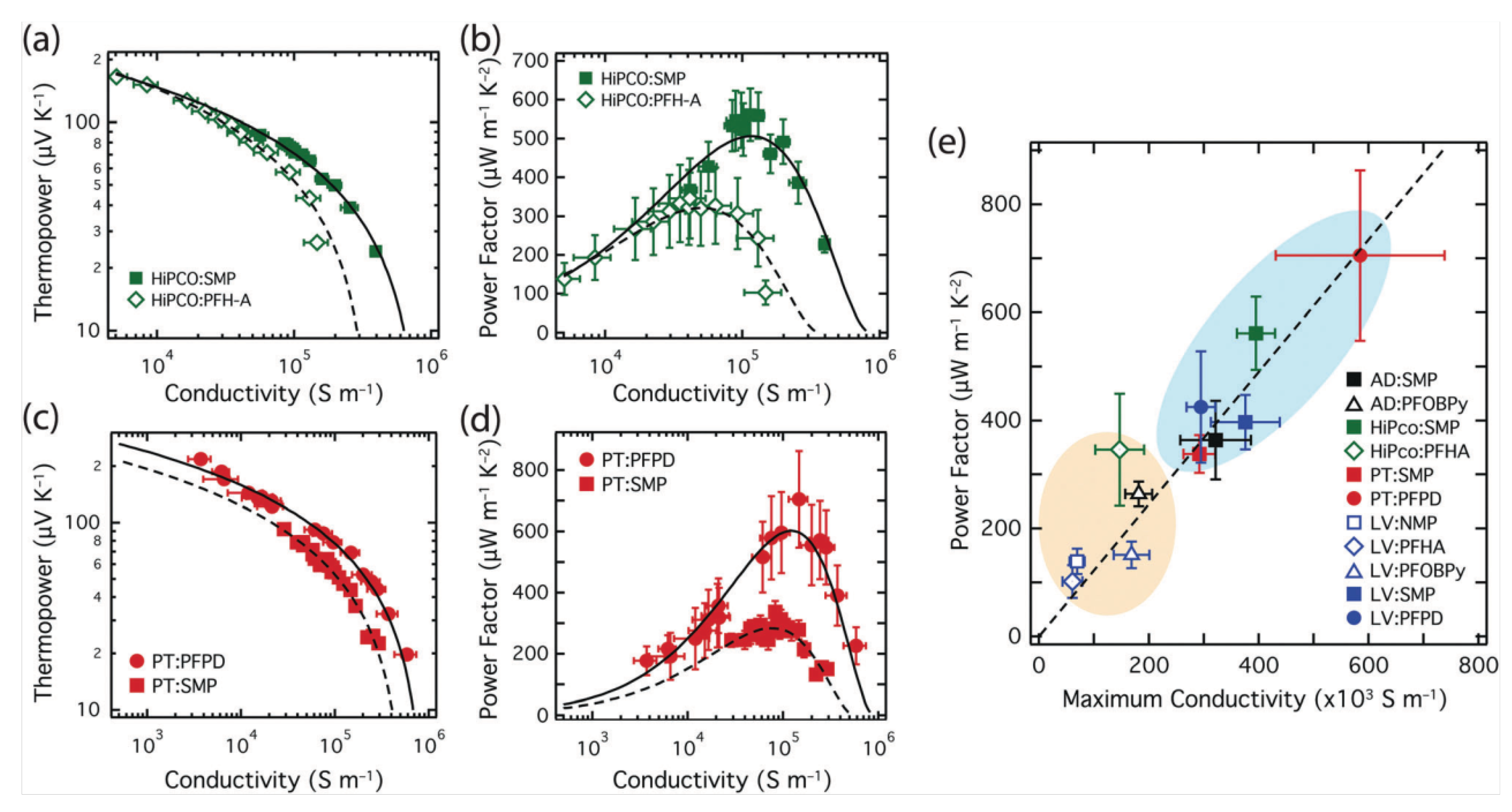
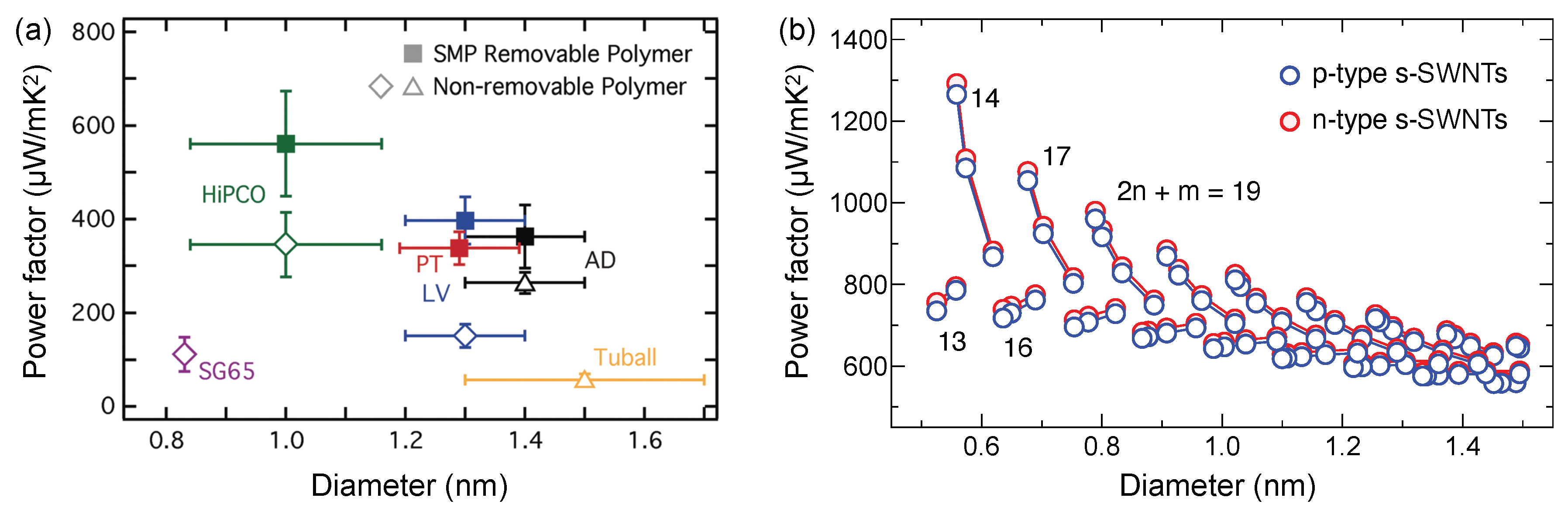
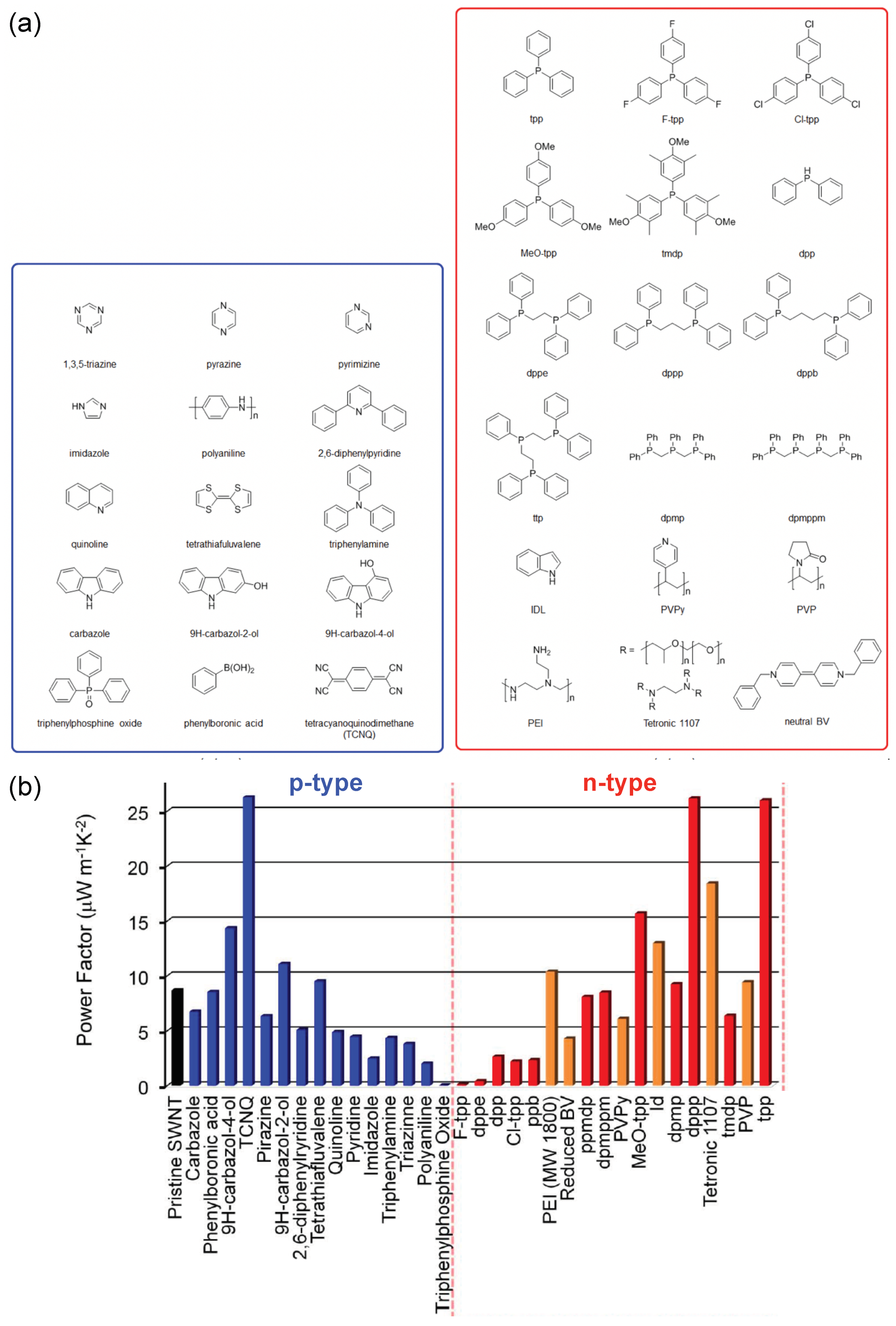
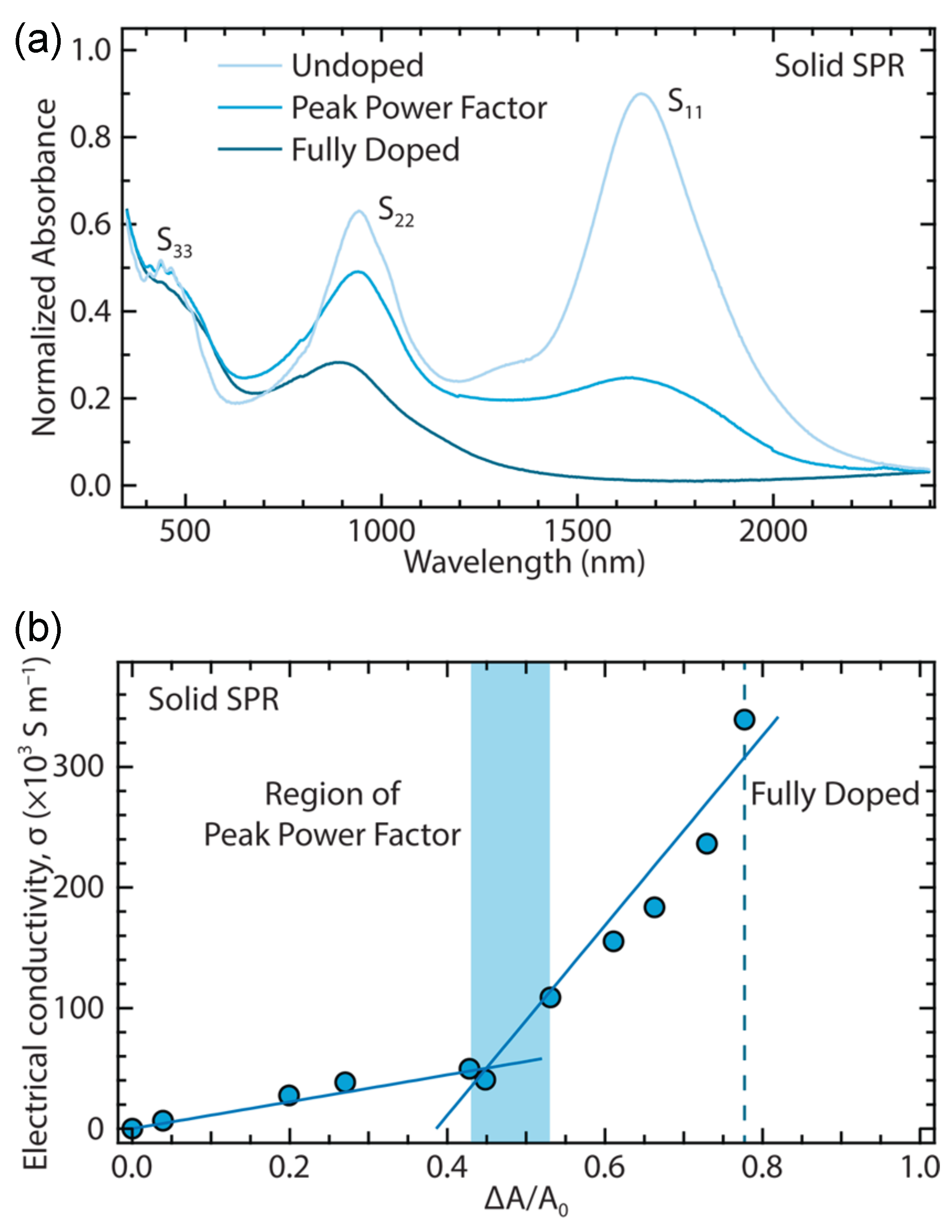
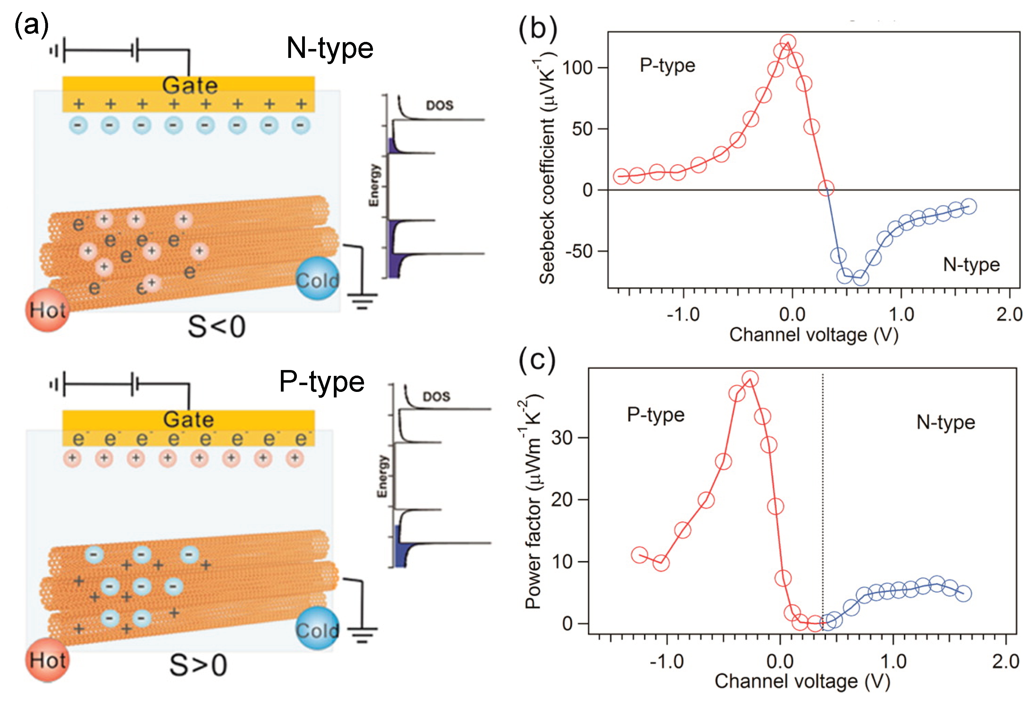
4.1. Optimizing Power Factor by Controlling Doping
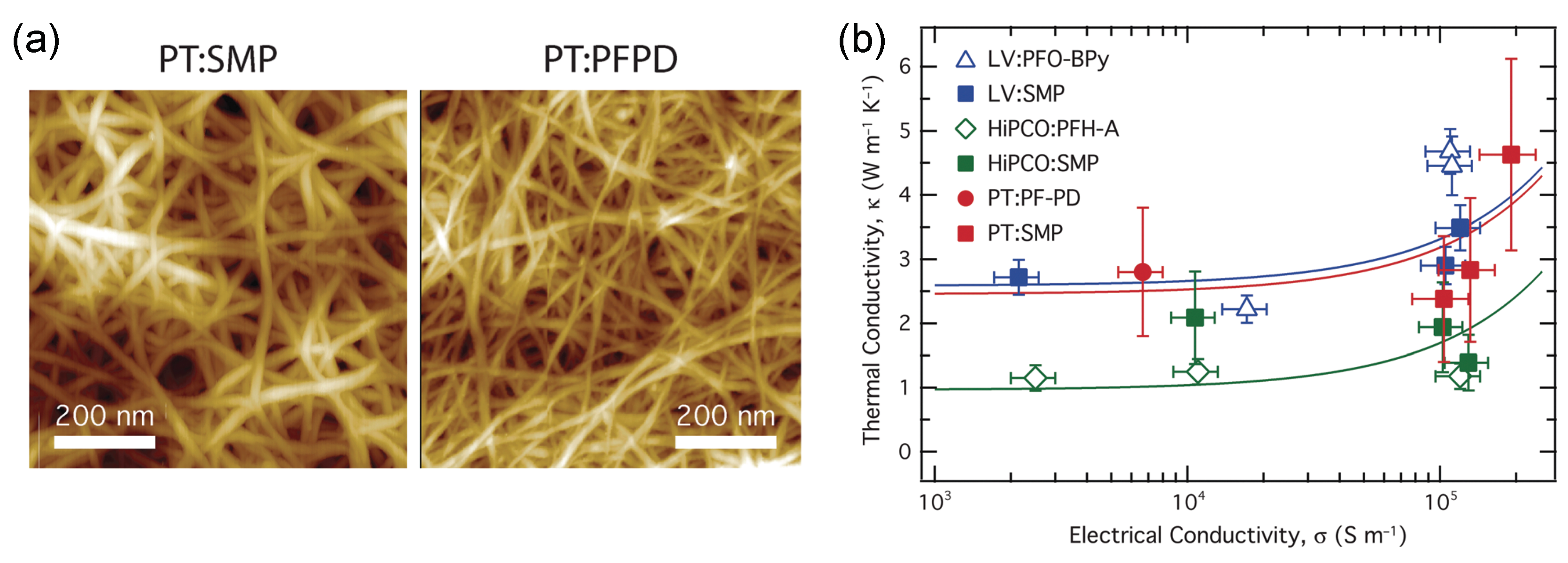
4.2. Reducing Thermal Conductivity by Using SWNT Networks
4.3. Figure of Merit of BiTe-SWNT Hybrid
5. Summary and Perspective
Author Contributions
Funding
Acknowledgments
Conflicts of Interest
Abbreviations
| CNT | carbon nanotube |
| SWNT | single wall carbon nanotube |
| s-SWNT | semiconducting single wall carbon nanotube |
| TE | thermoelectric |
| PF | power factor |
| optimized power factor | |
| optimized power factor of 3D system | |
| DOS | density of states |
| 1D | one-dimensional |
| 2D | two-dimensional |
| 3D | three-dimensional |
| KE | kinetic energy |
| CRTA | constant-relaxation-time approximation |
| STB | simple tight binding |
| ETB | extended tight binding |
| TW | twisting phonon mode |
| OA | triethyloxonium hexachloroantimonate |
| SMP | supramolecular polymer |
| HiPCO | high-pressure disproportionation of carbon monoxide |
| PT | plasma-torch |
| LV | laser vaporization |
| MFP | mean free path |
References
- Estimated U.S. Energy Consumption in 2018. Available online: https://flowcharts.llnl.gov/commodities/energy (accessed on 11 November 2019).
- Rowe, D.M. Thermoelectrics Handbook: Macro to Nano; CRC Press: Boca Ratcon, FL, USA, 2005. [Google Scholar]
- Vining, C.B. Semiconductors are cool. Nature 2001, 413, 577–578. [Google Scholar] [CrossRef] [PubMed]
- Goldsmid, H.J. Introduction to Thermoelectricity; Springer: Berlin/Heidelberg, Germany, 2010. [Google Scholar]
- Liu, W.; Kim, H.S.; Chen, S.; Jie, Q.; Lv, B.; Yao, M.; Ren, Z.; Opeil, C.P.; Wilson, S.; Chu, C.W.; et al. n-type thermoelectric material Mg2Sn0.75Ge0.25 for high power generation. Proc. Natl. Acad. Sci. USA 2015, 112, 3269–3274. [Google Scholar] [CrossRef] [PubMed]
- Liu, W.; Kim, H.S.; Jie, Q.; Ren, Z. Importance of high power factor in thermoelectric materials for power generation application: A perspective. Scr. Mater. 2016, 111, 3–9. [Google Scholar] [CrossRef]
- Yee, S.K.; LeBlanc, S.; Goodson, K.E.; Dames, C. $ per W metrics for thermoelectric power generation: beyond ZT. Energy Environ. Sci. 2013, 6, 2561–2571. [Google Scholar] [CrossRef]
- Ziman, J.M. Electrons and Phonons; Oxford University Press: Oxford, UK, 1960. [Google Scholar]
- Hicks, L.D.; Dresselhaus, M.S. Effect of quantum-well structures on the thermoelectric figure of merit. Phys. Rev. B 1993, 47, 12727. [Google Scholar] [CrossRef]
- Hicks, L.D.; Dresselhaus, M.S. Thermoelectric figure of merit of a one-dimensional conductor. Phys. Rev. B 1993, 47, 16631. [Google Scholar] [CrossRef]
- Boukai, A.I.; Bunimovich, Y.; Tahir-Kheli, J.; Yu, J.K.; Goddard Iii, W.A.; Heath, J.R. Silicon nanowires as efficient thermoelectric materials. Nature 2008, 451, 168–171. [Google Scholar] [CrossRef]
- Hochbaum, A.I.; Chen, R.; Delgado, R.D.; Liang, W.; Garnett, E.C.; Najarian, M.; Majumdar, A.; Yang, P. Enhanced thermoelectric performance of rough silicon nanowires. Nature 2008, 451, 163–167. [Google Scholar] [CrossRef]
- Hung, N.T.; Hasdeo, E.H.; Nugraha, A.R.T.; Dresselhaus, M.S.; Saito, R. Quantum Effects in the Thermoelectric Power Factor of Low-Dimensional Semiconductors. Phys. Rev. Lett. 2016, 117, 036602. [Google Scholar] [CrossRef]
- Hung, N.T.; Nugraha, A.R.T.; Saito, R. Size effect in thermoelectric power factor of nondegenerate and degenerate low-dimensional semiconductors. Mater. Today Proc. 2017, 4, 12368–12373. [Google Scholar] [CrossRef]
- Zeng, J.; He, X.; Liang, S.J.; Liu, E.; Sun, Y.; Pan, C.; Wang, Y.; Cao, T.; Liu, X.; Wang, C.; et al. Experimental identification of critical condition for drastically enhancing thermoelectric power factor of two-dimensional layered materials. Nano Lett. 2018, 18, 7538–7545. [Google Scholar] [CrossRef] [PubMed]
- Zhang, Y.; Feng, B.; Hayashi, H.; Chang, C.P.; Sheu, Y.M.; Tanaka, I.; Ikuhara, Y.; Ohta, H. Double thermoelectric power factor of a 2D electron system. Nat. Commun. 2018, 9, 2224. [Google Scholar] [CrossRef] [PubMed]
- Ohta, H.; Kim, S.; Mune, Y.; Mizoguchi, T.; Nomura, K.; Ohta, S.; Nomura, T.; Nakanishi, Y.; Ikuhara, Y.; Hirano, M.; et al. Giant thermoelectric Seebeck coefficient of a two-dimensional electron gas in SrTiO 3. Nat. Mater. 2007, 6, 129. [Google Scholar] [CrossRef] [PubMed]
- Ohta, H.; Kim, S.W.; Kaneki, S.; Yamamoto, A.; Hashizume, T. High Thermoelectric Power Factor of High-Mobility 2D Electron Gas. Adv. Sci. 2018, 5, 1700696. [Google Scholar] [CrossRef]
- Saito, R.; Dresselhaus, G.; Dresselhaus, M.S. Physical Properties of Carbon Nanotubes; World Scientific: London, UK, 1998. [Google Scholar]
- Poudel, B.; Hao, Q.; Ma, Y.; Lan, Y.; Minnich, A.; Yu, B.; Yan, X.; Wang, D.; Muto, A.; Vashaee, D.; et al. High-thermoelectric performance of nanostructured bismuth antimony telluride bulk alloys. Science 2008, 320, 634–638. [Google Scholar] [CrossRef]
- Heremans, J.P.; Jovovic, V.; Toberer, E.S.; Saramat, A.; Kurosaki, K.; Charoenphakdee, A.; Yamanaka, S.; Snyder, G.J. Enhancement of thermoelectric efficiency in PbTe by distortion of the electronic density of states. Science 2008, 321, 554–557. [Google Scholar] [CrossRef]
- Bubnova, O.; Khan, Z.U.; Malti, A.; Braun, S.; Fahlman, M.; Berggren, M.; Crispin, X. Optimization of the thermoelectric figure of merit in the conducting polymer poly (3, 4-ethylenedioxythiophene). Nat. Mater. 2011, 10, 429. [Google Scholar] [CrossRef]
- Lee, S.H.; Park, H.; Kim, S.; Son, W.; Cheong, I.W.; Kim, J.H. Transparent and flexible organic semiconductor nanofilms with enhanced thermoelectric efficiency. J. Mater. Chem. A 2014, 2, 7288–7294. [Google Scholar] [CrossRef]
- Kim, G.H.; Shao, L.; Zhang, K.; Pipe, K.P. Engineered doping of organic semiconductors for enhanced thermoelectric efficiency. Nat. Mater. 2013, 12, 719. [Google Scholar] [CrossRef]
- Berber, S.; Kwon, Y.K.; Tománek, D. Unusually high thermal conductivity of carbon nanotubes. Phys. Rev. Lett. 2000, 84, 4613. [Google Scholar] [CrossRef]
- Avery, A.D.; Zhou, B.H.; Lee, J.; Lee, E.S.; Miller, E.M.; Ihly, R.; Wesenberg, D.; Mistry, K.S.; Guillot, S.L.; Zink, B.L.; et al. Tailored semiconducting carbon nanotube networks with enhanced thermoelectric properties. Nat. Energy 2016, 1, 16033. [Google Scholar] [CrossRef]
- MacLeod, B.A.; Stanton, N.J.; Gould, I.E.; Wesenberg, D.; Ihly, R.; Owczarczyk, Z.R.; Hurst, K.E.; Fewox, C.S.; Folmar, C.N.; Hughes, K.H.; et al. Large n-and p-type thermoelectric power factors from doped semiconducting single-walled carbon nanotube thin films. Energy Environ. Sci. 2017, 10, 2168–2179. [Google Scholar] [CrossRef]
- Tortorich, R.P.; Choi, J.W. Inkjet printing of carbon nanotubes. Nanomaterials 2013, 3, 453–468. [Google Scholar] [CrossRef] [PubMed]
- Brownlie, L.; Shapter, J. Advances in carbon nanotube n-type doping: Methods, analysis and applications. Carbon 2018, 126, 257–270. [Google Scholar] [CrossRef]
- Derycke, V.; Martel, R.; Appenzeller, J.; Avouris, P. Controlling doping and carrier injection in carbon nanotube transistors. Appl. Phys. Lett. 2002, 80, 2773–2775. [Google Scholar] [CrossRef]
- Hung, N.T.; Nugraha, A.R.T.; Hasdeo, E.H.; Dresselhaus, M.S.; Saito, R. Diameter dependence of thermoelectric power of semiconducting carbon nanotubes. Phys. Rev. B 2015, 92, 165426. [Google Scholar] [CrossRef]
- Snyder, G.J.; Christensen, M.; Nishibori, E.; Caillat, T.; Iversen, B.B. Disordered zinc in Zn 4 Sb 3 with phonon-glass and electron-crystal thermoelectric properties. Nat. Mater. 2004, 3, 458. [Google Scholar] [CrossRef]
- Beekman, M.; Morelli, D.T.; Nolas, G.S. Better thermoelectrics through glass-like crystals. Nat. Mater. 2015, 14, 1182. [Google Scholar] [CrossRef]
- Takabatake, T.; Suekuni, K.; Nakayama, T.; Kaneshita, E. Phonon-glass electron-crystal thermoelectric clathrates: Experiments and theory. Rev. Mod. Phys. 2014, 86, 669. [Google Scholar] [CrossRef]
- Ma, J.; Delaire, O.; May, A.F.; Carlton, C.E.; McGuire, M.A.; VanBebber, L.H.; Abernathy, D.L.; Ehlers, G.; Hong, T.; Huq, A.; et al. Glass-like phonon scattering from a spontaneous nanostructure in AgSbTe 2. Nat. Nanotechnol. 2013, 8, 445. [Google Scholar] [CrossRef]
- Nielsen, M.D.; Ozolins, V.; Heremans, J.P. Lone pair electrons minimize lattice thermal conductivity. Energy Environ. Sci. 2013, 6, 570–578. [Google Scholar] [CrossRef]
- Hockings, E. The thermal conductivity of silver antimony telluride. J. Phys. Chem. Solids 1959, 10, 341–342. [Google Scholar] [CrossRef]
- Mukhopadhyay, S.; Parker, D.S.; Sales, B.C.; Puretzky, A.A.; McGuire, M.A.; Lindsay, L. Two-channel model for ultralow thermal conductivity of crystalline Tl3VSe4. Science 2018, 360, 1455–1458. [Google Scholar] [CrossRef] [PubMed]
- Hicks, L.D.; Harman, T.C.; Sun, X.; Dresselhaus, M.S. Experimental study of the effect of quantum-well structures on the thermoelectric figure of merit. Phys. Rev. B 1996, 53, R10493. [Google Scholar] [CrossRef]
- Majumdar, A. Thermoelectricity in semiconductor nanostructures. Science 2004, 303, 777–778. [Google Scholar] [CrossRef]
- Harman, T.C.; Spears, D.L.; Manfra, M.J. High thermoelectric figures of merit in PbTe quantum wells. J. Electron. Mater. 1996, 25, 1121–1127. [Google Scholar] [CrossRef]
- Sun, X.; Cronin, S.B.; Liu, J.; Wang, K.L.; Koga, T.; Dresselhaus, M.S.; Chen, G. Experimental study of the effect of the quantum well structures on the thermoelectric figure of merit in Si/Si1-xGex system. In Proceedings of the IEEE 18th International Conference Thermoelectrics, Baltimore, MD, USA, 29 August–2 September 1999; pp. 652–655. [Google Scholar]
- Kim, J.; Lee, S.; Brovman, Y.M.; Kim, P.; Lee, W. Diameter-dependent thermoelectric figure of merit in single-crystalline Bi nanowires. Nanoscale 2015, 7, 5053–5059. [Google Scholar] [CrossRef]
- Cheung, C.L.; Kurtz, A.; Park, H.; Lieber, C.M. Diameter-controlled synthesis of carbon nanotubes. J. Phys. Chem. B 2002, 106, 2429–2433. [Google Scholar] [CrossRef]
- Thurakitseree, T.; Kramberger, C.; Zhao, P.; Aikawa, S.; Harish, S.; Chiashi, S.; Einarsson, E.; Maruyama, S. Diameter-controlled and nitrogen-doped vertically aligned single-walled carbon nanotubes. Carbon 2012, 50, 2635–2640. [Google Scholar] [CrossRef]
- Saito, R.; Nugraha, A.R.T.; Hasdeo, E.H.; Hung, N.T.; Izumida, W. Electronic and optical properties of single wall carbon nanotubes. In Single-Walled Carbon Nanotubes; Springer: Berlin, Germany, 2019; pp. 165–188. [Google Scholar]
- Small, J.P.; Perez, K.M.; Kim, P. Modulation of thermoelectric power of individual carbon nanotubes. Phys. Rev. Lett. 2003, 91, 256801. [Google Scholar] [CrossRef]
- Hone, J.; Ellwood, I.; Muno, M.; Mizel, A.; Cohen, M.L.; Zettl, A.; Rinzler, A.G.; Smalley, R.E. Thermoelectric power of single-walled carbon nanotubes. Phys. Rev. Lett. 1998, 80, 1042. [Google Scholar] [CrossRef]
- Sumanasekera, G.U.; Adu, C.K.W.; Fang, S.; Eklund, P.C. Effects of gas adsorption and collisions on electrical transport in single-walled carbon nanotubes. Phys. Rev. Lett. 2000, 85, 1096. [Google Scholar] [CrossRef] [PubMed]
- Vavro, J.; Llaguno, M.C.; Satishkumar, B.C.; Luzzi, D.E.; Fischer, J.E. Electrical and thermal properties of C 60-filled single-wall carbon nanotubes. Appl. Phys. Lett. 2002, 80, 1450–1452. [Google Scholar] [CrossRef]
- Zhou, W.; Vavro, J.; Nemes, N.M.; Fischer, J.E.; Borondics, F.; Kamaras, K.; Tanner, D.B. Charge transfer and Fermi level shift in p-doped single-walled carbon nanotubes. Phys. Rev. B 2005, 71, 205423. [Google Scholar] [CrossRef]
- Yu, C.; Shi, L.; Yao, Z.; Li, D.; Majumdar, A. Thermal conductance and thermopower of an individual single-wall carbon nanotube. Nano Lett. 2005, 5, 1842–1846. [Google Scholar] [CrossRef] [PubMed]
- Nonoguchi, Y.; Ohashi, K.; Kanazawa, R.; Ashiba, K.; Hata, K.; Nakagawa, T.; Adachi, C.; Tanase, T.; Kawai, T. Systematic conversion of single walled carbon nanotubes into n-type thermoelectric materials by molecular dopants. Sci. Rep. 2013, 3, 3344. [Google Scholar] [CrossRef]
- Nakai, Y.; Honda, K.; Yanagi, K.; Kataura, H.; Kato, T.; Yamamoto, T.; Maniwa, Y. Giant Seebeck coefficient in semiconducting single-wall carbon nanotube film. Appl. Phys. Express 2014, 7, 025103. [Google Scholar] [CrossRef]
- Piao, M.; Joo, M.K.; Na, J.; Kim, Y.J.; Mouis, M.; Ghibaudo, G.; Roth, S.; Kim, W.Y.; Jang, H.K.; Kennedy, G.P.; et al. Effect of intertube junctions on the thermoelectric power of monodispersed single walled carbon nanotube networks. J. Phys. Chem. C 2014, 118, 26454–26461. [Google Scholar] [CrossRef]
- Zhou, W.; Fan, Q.; Zhang, Q.; Li, K.; Cai, L.; Gu, X.; Yang, F.; Zhang, N.; Xiao, Z.; Chen, H.; et al. Ultrahigh-power-factor carbon nanotubes and an ingenious strategy for thermoelectric performance evaluation. Small 2016, 12, 3407–3414. [Google Scholar] [CrossRef]
- Norton-Baker, B.; Ihly, R.; Gould, I.E.; Avery, A.D.; Owczarczyk, Z.R.; Ferguson, A.J.; Blackburn, J.L. Polymer-free carbon nanotube thermoelectrics with improved charge carrier transport and power factor. ACS Energy Lett. 2016, 1, 1212–1220. [Google Scholar] [CrossRef]
- Nonoguchi, Y.; Nakano, M.; Murayama, T.; Hagino, H.; Hama, S.; Miyazaki, K.; Matsubara, R.; Nakamura, M.; Kawai, T. Simple salt-coordinated n-type nanocarbon materials stable in air. Adv. Funct. Mater. 2016, 26, 3021–3028. [Google Scholar] [CrossRef]
- Zhou, W.; Fan, Q.; Zhang, Q.; Cai, L.; Li, K.; Gu, X.; Yang, F.; Zhang, N.; Wang, Y.; Liu, H.; et al. High-performance and compact-designed flexible thermoelectric modules enabled by a reticulate carbon nanotube architecture. Nat. Commun. 2017, 8, 14886. [Google Scholar] [CrossRef] [PubMed]
- Blackburn, J.L.; Kang, S.D.; Roos, M.J.; Norton-Baker, B.; Miller, E.M.; Ferguson, A.J. Intrinsic and extrinsically limited thermoelectric transport within semiconducting single-walled carbon nanotube networks. Adv. Electron. Mater. 2019, 28, 1800910. [Google Scholar] [CrossRef]
- Nakashima, Y.; Nakashima, N.; Fujigaya, T. Development of air-stable n-type single-walled carbon nanotubes by doping with 2-(2-methoxyphenyl)-1, 3-dimethyl-2, 3-dihydro-1H-benzo[d] imidazole and their thermoelectric properties. Synth. Met. 2017, 225, 76–80. [Google Scholar] [CrossRef]
- Samsonidze, G.G. Photophysics of Carbon Nanotubes. Ph.D. Thesis, MIT, Cambridge, MA, USA, 2006. [Google Scholar]
- Saito, R.; Sato, K.; Oyama, Y.; Jiang, J.; Samsonidze, G.G.; Dresselhaus, G.; Dresselhaus, M.S. Cutting lines near the Fermi energy of single-wall carbon nanotubes. Phys. Rev. B 2005, 72, 153413. [Google Scholar] [CrossRef]
- Nugraha, A.R.T. Coherent Phonon Spectroscopy of Carbon Nanotubes and Graphene. Ph.D. Thesis, Tohoku University, Sendai, Miyagi, Japan, 2013. [Google Scholar]
- Saito, R.; Dresselhaus, G.; Dresselhaus, M.S. Trigonal warping effect of carbon nanotubes. Phys. Rev. B 2000, 61, 2981. [Google Scholar] [CrossRef]
- Hung, N.T.; Nugraha, A.R.T.; Saito, R. Universal curve of optimum thermoelectric figures of merit for bulk and low-dimensional semiconductors. Phys. Rev. Appl. 2018, 9, 024019. [Google Scholar] [CrossRef]
- Yanagi, K.; Kanda, S.; Oshima, Y.; Kitamura, Y.; Kawai, H.; Yamamoto, T.; Takenobu, T.; Nakai, Y.; Maniwa, Y. Tuning of the thermoelectric properties of one-dimensional material networks by electric double layer techniques using ionic liquids. Nano Lett. 2014, 14, 6437–6442. [Google Scholar] [CrossRef]
- Goldsmid, H.J.; Sharp, J.W. Estimation of the thermal band gap of a semiconductor from Seebeck measurements. J. Electron. Mater. 1999, 28, 869–872. [Google Scholar] [CrossRef]
- Stradling, R.A.; Wood, R.A. The temperature dependence of the band-edge effective masses of InSb, InAs and GaAs as deduced from magnetophonon magnetoresistance measurements. J. Phys. C Solid State Phys. 1970, 3, L94. [Google Scholar] [CrossRef]
- Pei, Y.; Shi, X.; LaLonde, A.; Wang, H.; Chen, L.; Snyder, G.J. Convergence of electronic bands for high performance bulk thermoelectrics. Nature 2011, 473, 66–69. [Google Scholar] [CrossRef] [PubMed]
- Kataura, H.; Kumazawa, Y.; Maniwa, Y.; Umezu, I.; Suzuki, S.; Ohtsuka, Y.; Achiba, Y. Optical properties of single-wall carbon nanotubes. Synth. Met. 1999, 103, 2555–2558. [Google Scholar] [CrossRef]
- Weisman, R.B.; Bachilo, S.M. Dependence of optical transition energies on structure for single-walled carbon nanotubes in aqueous suspension: an empirical Kataura plot. Nano Lett. 2003, 3, 1235–1238. [Google Scholar] [CrossRef]
- Mateeva, N.; Niculescu, H.; Schlenoff, J.; Testardi, L.R. Correlation of Seebeck coefficient and electric conductivity in polyaniline and polypyrrole. J. Appl. Phys. 1998, 83, 3111–3117. [Google Scholar] [CrossRef]
- Heikes, R.R.; Ure, R.W. Thermoelectricity: Science and Engineering; Interscience Publishers: New York, NY, USA, 1961. [Google Scholar]
- Chandra, B.; Afzali, A.; Khare, N.; El-Ashry, M.M.; Tulevski, G.S. Stable charge-transfer doping of transparent single-walled carbon nanotube films. Chem. Mater. 2010, 22, 5179–5183. [Google Scholar] [CrossRef]
- Jones, W.; March, N.H. Theoretical Solid State Physics; Courier Corporation: North Chelmsford, MA, USA, 1985; Volume 35. [Google Scholar]
- Matula, R.A. Electrical resistivity of copper, gold, palladium, and silver. J. Phys. Chem. Ref. Data 1979, 8, 1147–1298. [Google Scholar] [CrossRef]
- Hone, J.; Whitney, M.; Piskoti, C.; Zettl, A. Thermal conductivity of single-walled carbon nanotubes. Phys. Rev. B 1999, 59, R2514. [Google Scholar] [CrossRef]
- Zhao, X.; Huang, C.; Liu, Q.; Smalyukh, I.I.; Yang, R. Thermal conductivity model for nanofiber networks. J. Appl. Phys. 2018, 123, 085103. [Google Scholar] [CrossRef]
- Kittel, C. Introduction to Solid State Physics; Wiley: New York, NY, USA, 1976; Volume 8. [Google Scholar]
- Pop, E.; Mann, D.; Wang, Q.; Goodson, K.; Dai, H. Thermal conductance of an individual single-wall carbon nanotube above room temperature. Nano Lett. 2006, 6, 96–100. [Google Scholar] [CrossRef]
- Chen, S.; Wu, Q.; Mishra, C.; Kang, J.; Zhang, H.; Cho, K.; Cai, W.; Balandin, A.A.; Ruoff, R.S. Thermal conductivity of isotopically modified graphene. Nat. Mater. 2012, 11, 203. [Google Scholar] [CrossRef]
- Klemens, P.G. Thermal conductivity and lattice vibrational modes. Sol. Stat. Phys. 1958, 7, 1–98. [Google Scholar]
- Lindsay, L.; Broido, D.A.; Mingo, N. Flexural phonons and thermal transport in graphene. Phys. Rev. B 2010, 82, 115427. [Google Scholar] [CrossRef]
- Saito, R.; Mizuno, M.; Dresselhaus, M.S. Ballistic and diffusive thermal conductivity of graphene. Phys. Rev. Appl. 2018, 9, 024017. [Google Scholar] [CrossRef]
- Lindsay, L.; Broido, D.A.; Mingo, N. Diameter dependence of carbon nanotube thermal conductivity and extension to the graphene limit. Phys. Rev. B 2010, 82, 161402. [Google Scholar] [CrossRef]
- Zhang, H.L.; Li, J.F.; Zhang, B.P.; Yao, K.F.; Liu, W.S.; Wang, H. Electrical and thermal properties of carbon nanotube bulk materials: experimental studies for the 328–958 K temperature range. Phys. Rev. B 2007, 75, 205407. [Google Scholar] [CrossRef]
- Mistry, K.S.; Larsen, B.A.; Bergeson, J.D.; Barnes, T.M.; Teeter, G.; Engtrakul, C.; Blackburn, J.L. n-Type transparent conducting films of small molecule and polymer amine doped single-walled carbon nanotubes. ACS Nano 2011, 5, 3714–3723. [Google Scholar] [CrossRef]
- Cheng, X.; Wang, X.; Chen, G. A convenient and highly tunable way to n-type carbon nanotube thermoelectric composite film using common alkylammonium cationic surfactant. J. Mater. Chem. A 2018, 6, 19030–19037. [Google Scholar] [CrossRef]
- Shimizu, S.; Iizuka, T.; Kanahashi, K.; Pu, J.; Yanagi, K.; Takenobu, T.; Iwasa, Y. Thermoelectric detection of multi-subband density of states in semiconducting and metallic single-walled carbon nanotubes. Small 2016, 12, 3388–3392. [Google Scholar] [CrossRef]
- Hone, J.; Llaguno, M.C.; Nemes, N.M.; Johnson, A.T.; Fischer, J.E.; Walters, D.A.; Casavant, M.J.; Schmidt, J.; Smalley, R.E. Electrical and thermal transport properties of magnetically aligned single wall carbon nanotube films. Appl. Phys. Lett. 2000, 77, 666–668. [Google Scholar] [CrossRef]
- Chalopin, Y.; Volz, S.; Mingo, N. Upper bound to the thermal conductivity of carbon nanotube pellets. J. Appl. Phys. 2009, 105, 084301. [Google Scholar] [CrossRef]
- Prasher, R.S.; Hu, X.J.; Chalopin, Y.; Mingo, N.; Lofgreen, K.; Volz, S.; Cleri, F.; Keblinski, P. Turning carbon nanotubes from exceptional heat conductors into insulators. Phys. Rev. Lett. 2009, 102, 105901. [Google Scholar] [CrossRef] [PubMed]
- Kulbachinskii, V.A.; Kytin, V.G.; Kudryashov, A.A.; Tarasov, P.M. Thermoelectric properties of Bi2Te3, Sb2Te3 and Bi2Se3 single crystals with magnetic impurities. J. Solid State Chem. 2012, 193, 47–52. [Google Scholar] [CrossRef]
- Jin, Q.; Jiang, S.; Zhao, Y.; Wang, D.; Qiu, J.; Tang, D.M.; Tan, J.; Sun, D.M.; Hou, P.X.; Chen, X.Q.; et al. Flexible layer-structured Bi2Te3 thermoelectric on a carbon nanotube scaffold. Nat. Mater. 2019, 18, 62. [Google Scholar] [CrossRef] [PubMed]
- Wang, H.; Hsu, J.H.; Yi, S.I.; Kim, S.L.; Choi, K.; Yang, G.; Yu, C. Thermally driven large n-type voltage responses from hybrids of carbon nanotubes and poly (3, 4-ethylenedioxythiophene) with tetrakis (dimethylamino) ethylene. Adv. Mater. 2015, 27, 6855–6861. [Google Scholar] [CrossRef] [PubMed]


| Sample | Enrichment | S (V/K) | (1/cm) | PF (W/mK) | (W/mK) | Year | Ref. | |
|---|---|---|---|---|---|---|---|---|
| SWNT bundles | Metallic | 50 | – | – | – | – | 1988 | [48] |
| SWNT bundles | Metallic | 48 | – | – | – | – | 2000 | [49] |
| C-filled SWNTs | Metallic | 60 | – | – | 15 | – | 2002 | [50] |
| Individual SWNTs | Metallic Semiconductor | 35 260 | – – | – – | – – | – – | 2003 | [47] |
| Bulk SWNTs | – | 60 | 100 | – | – | – | 2005 | [51] |
| Individual SWNTs | Metallic | 42 | 4000 | – | – | – | 2005 | [52] |
| SWNT films (with different dopants) | – – – – – – – – – – – – – – – – | 49 88 56 54 53 52 47 46 44 41 41 34 34 33 27 2.0 | 35.7 8.7 27.7 49.7 94.0 23.2 50.7 23.8 49.2 28.2 26.6 21.5 38.7 34.3 28.5 32.2 | 8.6 6.7 8.7 14.5 26.4 6.3 11.2 5.0 9.5 4.7 4.5 2.5 4.5 3.7 2.1 0.01 | – – – – – – – – – – – – – – – – | – – – – – – – – – – – – – – – – | 2013 | [53] |
| SWNT films | Metallic Mix Semiconductor | 15 35 160 | 200 50 12.5 | 4.5 6.1 32 | – – – | – – – | 2014 | [54] |
| SWNT films | Metallic Semiconductor | 13 88 | 300 270 | 5.1 210 | – – | – – | 2014 | [55] |
| SWNT films (with different thickness) | Semiconductor | 88 59 78 | 3210 4740 3750 | 2482 1654 2280 | – – – | – – – | 2016 | [56] |
| SWNT films (with different dopants) | Semiconductor | 30 32.5 49 | 1690 3760 690 | 152 398 139 | 2.45 3.85 | 0.031 0.04 | 2016 | [57] |
| SWNT films | – | 38 | 1510 | 220 | 9.8 | 0.007 | 2016 | [58] |
| SWNT films | Semiconductor | 100 | 3400 | 340 | - | – | 2016 | [26] |
| SWNT films (with different synthesis methods) | Semiconductor | 84 70 69 | 512 1140 1475 | 363 562 706 | – 1.4 2.8 | – 0.12 0.08 | 2017 | [27] |
| SWNT films | Semiconductor | 78 | 3020 | 1840 | – | – | 2017 | [59] |
| SWNT films | Semiconductor | 52 | 1500 | 400 | – | – | 2019 | [60] |
| Sample | Enrichment | S (V/K) | (1/cm) | PF (W/mK) | (W/mK) | Year | Ref. | |
|---|---|---|---|---|---|---|---|---|
| SWNT bundles | Metallic | – | – | – | – | 2000 | [49] | |
| Individual SWNTs | Metallic | – | – | – | – | 2003 | [47] | |
| SWNT films (with different dopants) | – – – – – – – – – – – – – – – – – – | 29.6 21.5 43.5 26.2 25.8 89.7 32.8 49.8 44.3 27.2 64.8 50.4 35 98.1 66.6 22.7 33.3 49.8 | 0.1 0.4 2.7 2.2 2.3 10.4 4.3 8.0 8.6 6.0 15.6 13.1 9.5 26.5 18.7 6.4 9.4 16.5 | – – – – – – – – – – – – – – – – – – | – – – – – – – – – – – – – – – – – – | 2013 | [53] | |
| SWNT films | – | 2050 | 230 | 39 | 0.001 | 2016 | [58] | |
| SWNT films | – | 620 | 115 | 24.4 | 0.0017 | 2017 | [61] | |
| SWNT films | Semiconductor | 1190 | 730 | – | – | 2017 | [27] | |
| SWNT films | Semiconductor | 3630 | 1500 | – | – | 2017 | [59] |
© 2019 by the authors. Licensee MDPI, Basel, Switzerland. This article is an open access article distributed under the terms and conditions of the Creative Commons Attribution (CC BY) license (http://creativecommons.org/licenses/by/4.0/).
Share and Cite
T. Hung, N.; R. T. Nugraha, A.; Saito, R. Thermoelectric Properties of Carbon Nanotubes. Energies 2019, 12, 4561. https://doi.org/10.3390/en12234561
T. Hung N, R. T. Nugraha A, Saito R. Thermoelectric Properties of Carbon Nanotubes. Energies. 2019; 12(23):4561. https://doi.org/10.3390/en12234561
Chicago/Turabian StyleT. Hung, Nguyen, Ahmad R. T. Nugraha, and Riichiro Saito. 2019. "Thermoelectric Properties of Carbon Nanotubes" Energies 12, no. 23: 4561. https://doi.org/10.3390/en12234561
APA StyleT. Hung, N., R. T. Nugraha, A., & Saito, R. (2019). Thermoelectric Properties of Carbon Nanotubes. Energies, 12(23), 4561. https://doi.org/10.3390/en12234561