Article

Detection of Typical Defects in Silicon Photovoltaic Modules and Application for Plants with Distributed MPPT Configuration

1
Energy Department, Politecnico di Torino, corso Duca degli Abruzzi 24, 10129 Torino, Italy
2
Department of Electrical Engineering, University of Central Punjab, Lahore 54590, Pakistan
*
Author to whom correspondence should be addressed.
Energies 2019, 12(23), 4547; https://doi.org/10.3390/en12234547
Submission received: 21 October 2019 / Revised: 20 November 2019 / Accepted: 27 November 2019 / Published: 29 November 2019
(This article belongs to the Special Issue Photovoltaic Modules)

Abstract

:
During their operational life, photovoltaic (PV) modules may exhibit various defects for poor sorting of electrical performance during manufacturing, mishandling during transportation and installation, and severe thermo-mechanical stresses. Electroluminescence testing and infrared thermographic imaging are the most common tests for checking these defects, but they are only economically viable for large PV plants. The defects are also manifested as abnormal electrical properties of the affected PV modules. For defect diagnosis, the appropriate parameters on their I-V curves are open circuit voltage, photo-generated current, series resistance, and the shunt resistance. The health of PV modules can be assessed by calculating these values and comparing them with the reference parameters. If these defects are diagnosed in time, the power loss is avoided and safety hazards are mitigated. This paper first presents a review of common defects in PV modules and then a review of the methods used to find the above-mentioned parameters during the normal PV operation. A simple approach to determine the resistances of the equivalent circuit is discussed. Finally, through a modification in an ordinary maximum power point tracking (MPPT) algorithm, information about the state of health of PV modules is obtained. This method is effective, especially if applied to submodule-integrated MPPT architectures.

1. Introduction

Over the last few years, concerns about climate change, global warming, and gas emissions have pushed the policy makers toward the increase of renewable power generation, with a consequent rapid cost decline. This is reflected in growing investments in electricity generation from wind and solar power systems, such as photovoltaic (PV) and concentrated solar power (CSP) systems [1,2]. In particular, an enormous growth of installed PV plants has occurred: the installed capacity of PVs throughout the world was 5.1 GW in 2005 and increased to 227 GW by the end of 2015 [3]. It is anticipated that this trend is likely to continue, as demonstrated by various papers investigating the effect and potential application of PV for the electric system (e.g., references [4,5]).
Recently, many governments have offered incentives for the installation of solar power plants. Therefore, many PV modules have been manufactured in a rapid time frame, and, in many cases, the performance of the modules has been below the common standards [6]. Owing to this and a general lack of maintenance and proper vigilance, degradation in the performance of the PVs has been reported by operation and maintenance personnel. The failure of solar modules can be divided into three classes: infant mortality, midlife failure, and wear-out failure [7]. Furthermore, PV generators exhibit light-induced power degradation from the outset after installation.
Infant mortality failures take place shortly after the modules are installed in the field. The defective modules fail rapidly and have a significant effect on the costs for manufacturers and installers, as they are responsible for these defects. Midlife failures occur when the PVs remain operational in the field for many years and are subject to severe thermo-mechanical stresses. The failure of junction box and cables, hotspots and burnout marks on cells and backsheets of the PV modules, glass breakage, electrical disconnection of parts of cells due to cell breakage, encapsulant discoloration, damage to the interconnection ribbons, etc. lead to midlife failures. These defects not only degrade the performance of the PVs but can also lead to safety hazards. Wear-out faults determine the useful life of PV modules. The working life stops when a safety problem occurs or the power generation falls below a certain limit [7].
Even though PV technology has advanced, the substandard quality of cells and modules has raised concerns. There have been reports that many PV devices have failed in the field during the first two years and that the rate of module replacement has increased [3,6]. Thus, it is important to develop methods to identify the sources of faults in PV modules during on-field operation and to isolate and remove these failures [8]. The online detection and diagnosis of PV module’s faults has become a technical and economic challenge [9].

2. Tests for Identification of Defects in PV Generators

For the purpose of diagnosis of faults in solar arrays, three types of tests are the most important—infrared thermographic (IRT) imaging, electroluminescence (EL) imaging, and scanning the current-voltage (I-V) characteristic curve.

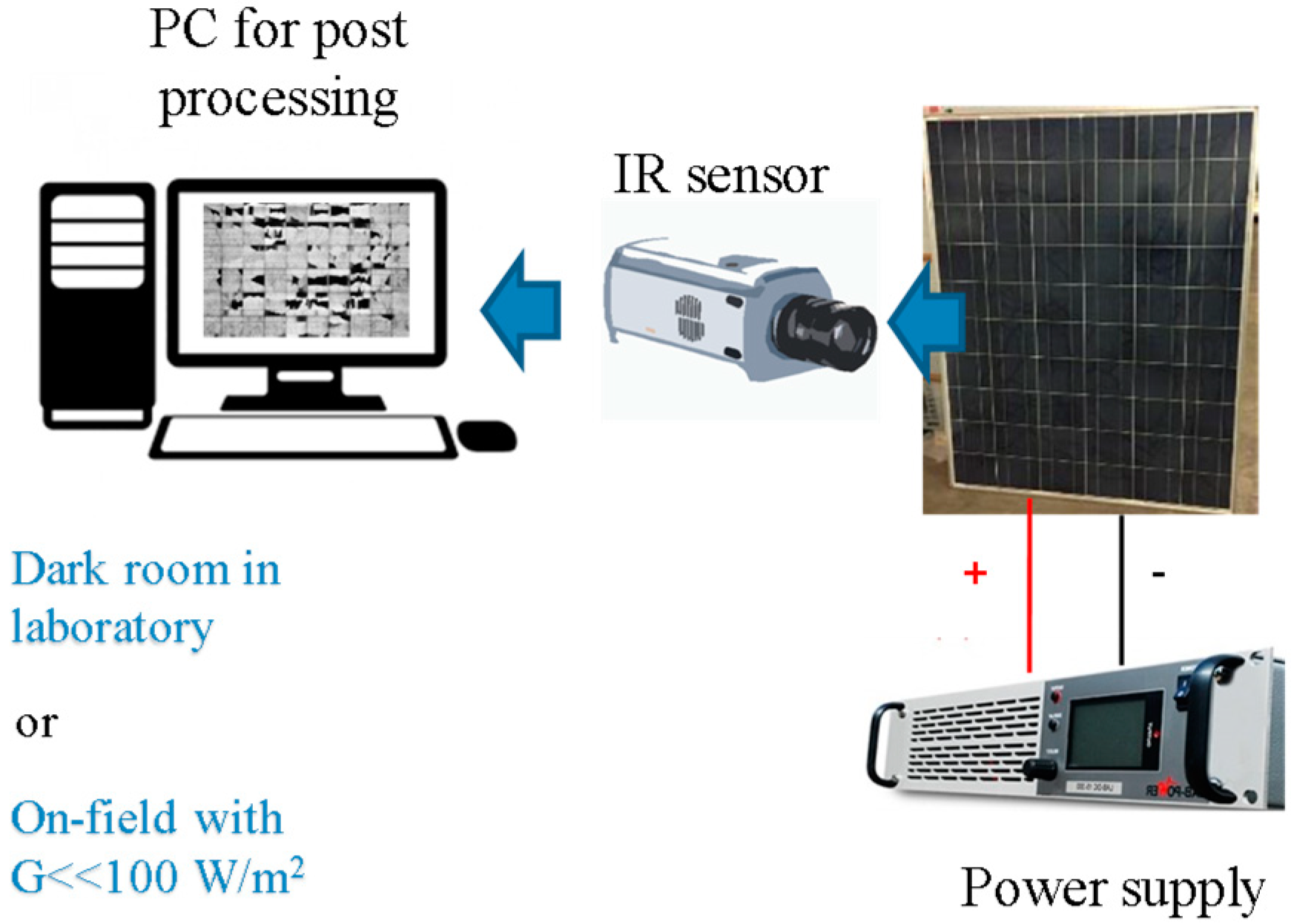
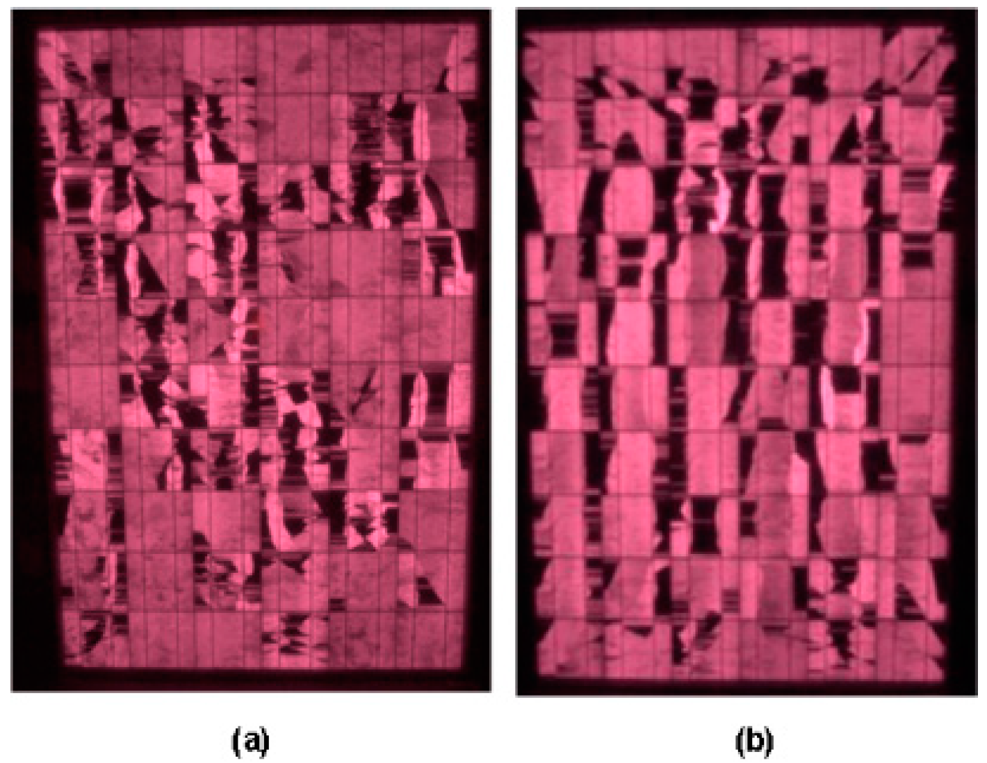
2.1. Infrared Thermographic and Electroluminescence Imaging

IRT and EL can find the presence of defects within a solar array and identify the exact location of faults [10,11]. IRT imaging offers real-time information of failures and defects in the PV modules. It provides qualitative information about the extent of the damage caused by a particular fault. The images of the body can be captured by an IR camera (in a wavelength range of 7–14 μm), and the temperature distribution can be measured from these images [12]. In PV applications, the thermography measurements are usually performed on clear, sunny days with irradiance > 700 W/m2. Ideally the wind speed should be low [7,13]. The images of the healthy PV modules that are obtained with this technique show uniform temperature distribution [14]. As some of the faults have a substantial effect on the thermal performance of the modules, those are identified as inhomogeneity in the image. These images can used for quantitative diagnosis in order to find the extent to which the damage is caused by the defect in terms of power loss. Even though the IRT imaging looks quite appealing, since the diagnosis can be done during PV operation [15], it still suffers the following disadvantages:
  • Thermal imaging only provides a qualitative diagnosis of the state of health of the PV modules, and it may require expert knowledge to be performed properly [16];
  • IR cameras with adequate specifications are expensive [17];
  • In the case of large power plants, a manual IRT inspection requires too much time and is expensive; thus, the use of unmanned drones equipped with IR camera could be necessary [6,8].
Compared to thermography, EL offers a considerably improved image resolution and level of detail [17,18]. In this case, the image of a PV module is obtained by inducing a current through it in the reverse direction. The image of the module is then captured. As shown in Figure 1, the EL test starts with the application of a forward bias to the PV generator, in a dark room (laboratory) or on-field with low irradiance (G < 100 W/m2). The crystalline silicon PV cells work like a light emitting diode, in which the semiconductors have emission spectra in the IR region (≈ 1000–1200 nm, and the peak, corresponding to the band gap, is 1150 nm) and not in the visible region. The emitted photons are detected by a sensitive camera equipped with indium gallium arsenide (InGaAs) photodiodes, or silicon devices, i.e., a silicon charge-coupled device (CCD) or complementary metal-oxide-semiconductor (CMOS.) [19,20].
EL images permit us to identify several types of faults in a module. However, the EL based diagnosis has the following limitations [8]:
  • The El test cannot be performed during PV operation;
  • In cases of optical degradation, glass breakage, or delamination, the EL test is less efficient;
  • As in case of IRT, the power loss of a defective module cannot be quantified.
In conclusion, the EL test provides more accurate information about the state of health of PV modules with respect to thermography. In fact, an EL image shows almost all the defects, even when there are no hot-spots or temperature gradients, because the defects are dispersed in all the cells. Nevertheless, EL is much more expensive and complex.

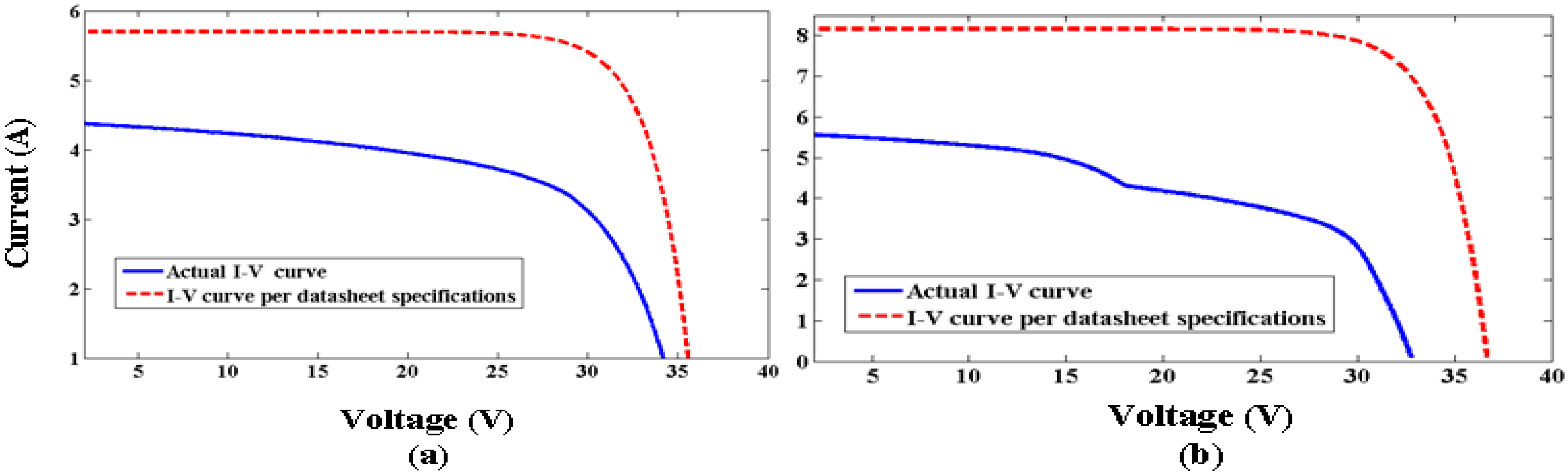
2.2. I-V Curve Characterization

The main alternative to the defect detection by image analysis is I-V curve characterization. The main difference with respect to IRT and EL imaging is that the I-V scan provides quantitative information about the state of health of the PV generator. In particular, thanks to the scan, the electrical parameters are measured, and the performance of the generator can be calculated. The scan can be carried out during MPP search by controlling the current generated by the PV module between the short circuit point (ISC) and the zero current point (VOC) [21]. The most important methods for scanning the I-V curve [21] are the following. The easiest way is the use of a resistive load with variable resistance; nevertheless, this method has a long duration because a resistance linearly varies from zero to infinity in order to scan the points of the I-V curve of the generator [22]. On the contrary, the tests are easily and rapidly performed by the transient charge of a capacitive load [23,24]. An external capacitor, initially discharged, is charged by the PV array from short-circuit to open-circuit conditions. The duration of the transient can be reduced if its capacitance is decreased. Another possible solution is the use of a DC/DC converter, which can behave like a resistor emulator, and the I-V curve of the generator can be traced by changing the duty cycle in a range of 0–1. However, the presence of various transistors and storage components (inductors and capacitors) increases their cost [25,26]. Finally, an electronic load [27], i.e., a transistor (generally, a metal-oxide semiconductor field-effect transistor, MOSFET) can be used to simulate a resistance. Its I-V curve varies not linearly with fast variations according to the gate-source voltage.
Starting from the data points after the scan of the I-V curve of a PV generator, the parameters short circuit current (ISC), open circuit voltage (VOC), shunt resistance (Rsh), series resistance (Rs), and fill factor (FF, ratio of maximum power to the product of ISC and VOC) can be assessed. These quantities are meaningful when performing the quantitative analysis of the defective modules. A brief summary of some of the defects that can be diagnosed from the abnormal I-V curve is as follows [7]:
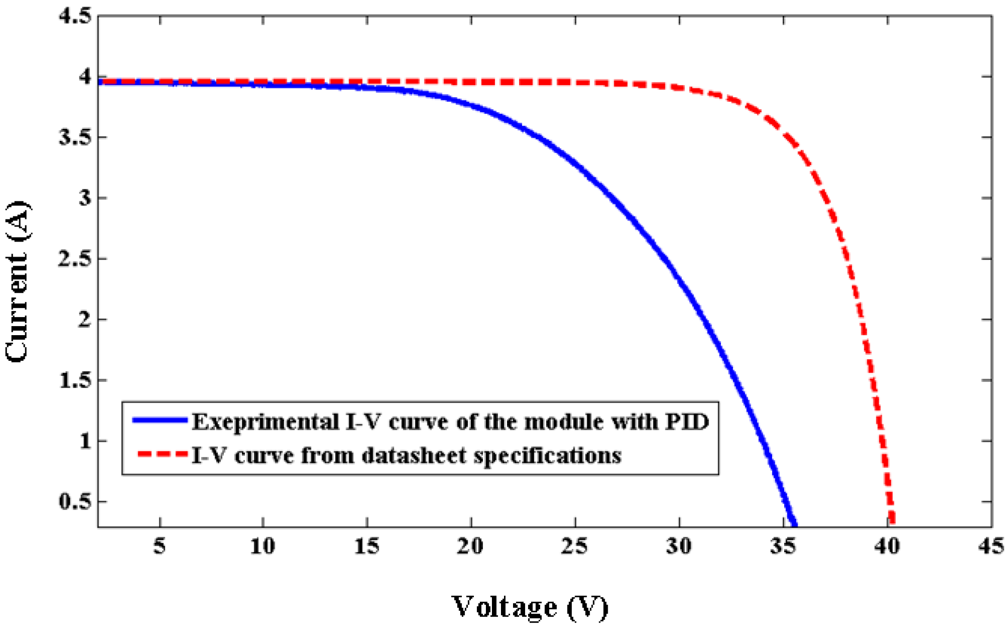
  • A lower ISC than the expected value may represent discoloration of encapsulation, glass corrosion, etc.;
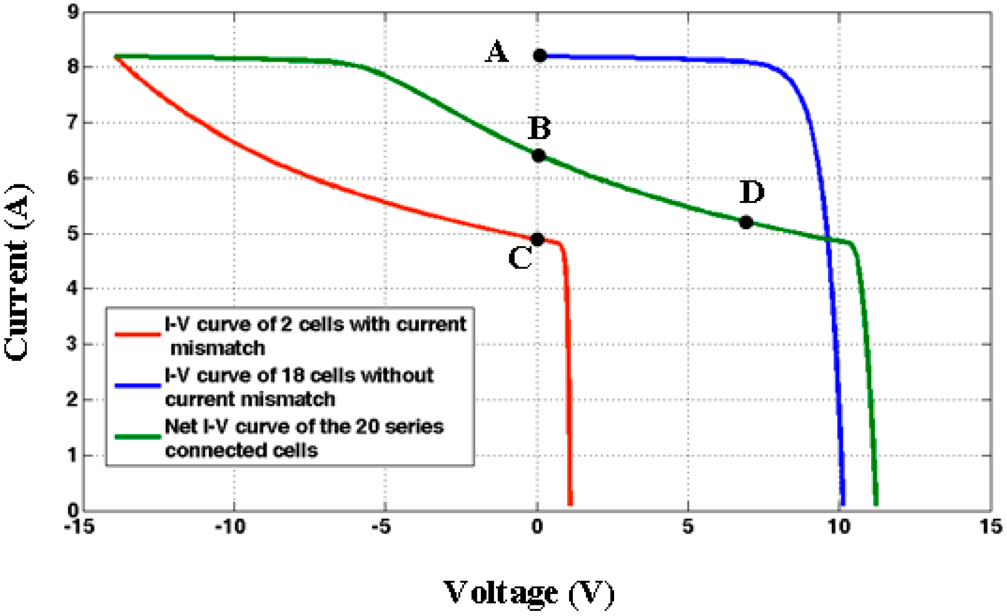
  • A stepped-shaped I-V curve usually represents the current mismatch that may be caused by damaged cells, gathering of soil over the surface, or partial shading;
  • A decrease in VOC shows the light induced degradation, the potential induced degradation, or shorted bypass diode;
  • Increased slope near the ISC can be due to the formation of shunt paths in the PV cells;
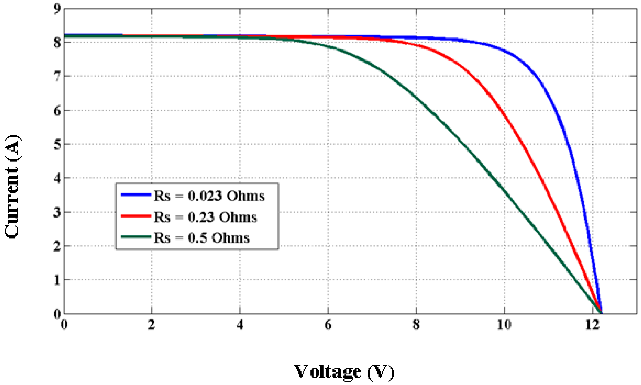
  • A lower value of the slope of the characteristic curve near the VOC usually suggests an increase of interconnection resistance, oxidization in the junction box, or damaged interconnecting ribbons.

3. Review of Common Defects in Silicon PV Modules

In this section, a review of common defects in the PV modules is presented. For some of these faults, the EL images of the module will be presented, and the effects of these defects on the electrical properties of the modules will be highlighted.
The common defects in the crystalline silicon modules are failure of ethylene vinyl acetate (EVA) encapsulation (3.1); cracks and micro-cracks (3.2), hot spots (3.3), disconnections (3.4), potential induced degradation (3.5) for the cells inside the modules, and defective bypass diodes (3.6).

3.1. Ethylene Vinyl Acetate (EVA) Failures
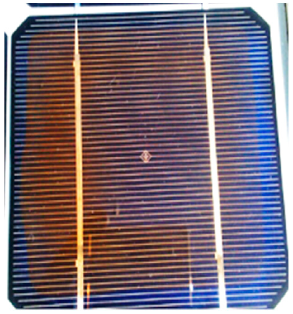
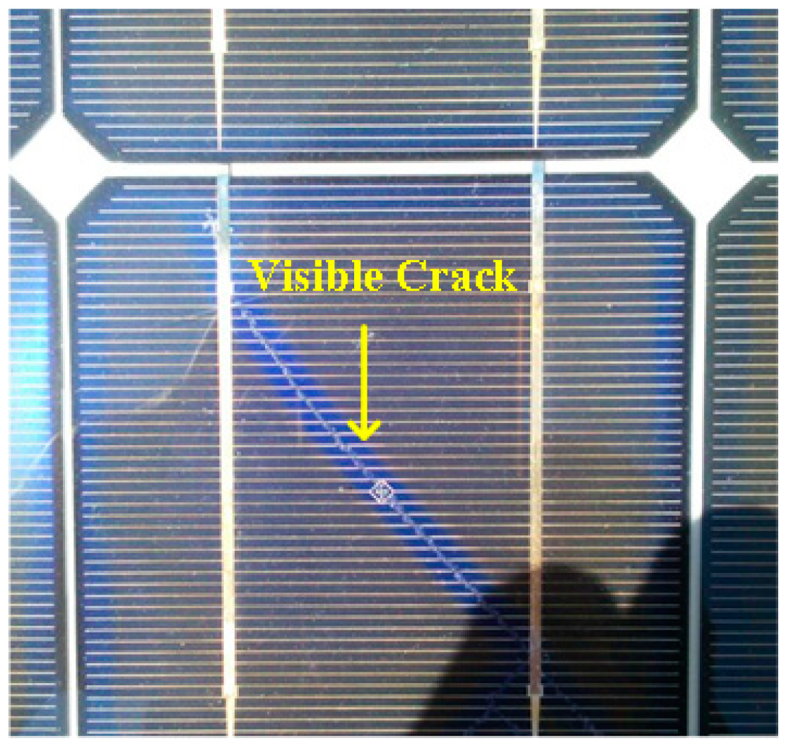
The yellowing and browning of the ethylene vinyl acetate (EVA) or other encapsulation materials is an easily identifiable defect when inspecting the modules with the naked eye. This fault is most common when the modules are exposed to ultraviolet (UV) radiation, high temperatures, and humidity for an extended duration of time or if the quality of the encapsulating material is low. According to reference [11], this type of degradation takes place at the junction of the EVA encapsulant and front of the PV cell and between the encapsulant and the glass cover. The material used in the manufacturing of the encapsulation (i.e., EVA) is treated under a defined temperature for an appropriate period of time and its life time depends, among other things, on the addition of UV stabilizers and anti-oxidants. Incorrect processing or substandard quality of the EVA encapsulant leads to three different failure modes—delamination, corrosion, and discoloration [28].
Delamination is caused by adhesion loss and the consequent separation of the EVA encapsulant and the substrate film of the PV module. This failure particularly occurs near the edges and corners of the module, leading to water infiltration that accelerates the corrosion process [29].
Corrosion is caused by the presence of acetic acid, resulting in EVA yellowing [30]. It affects the metallic contacts of the cell, the resistances in junction-box terminations and the cell-interconnect busbars reducing, in this way, the cell efficiency.
EVA discoloration is accompanied by a reduction in the ISC and the current at the MPP of the module. In reference [31], it is shown that this defect generally causes less than 0.5% per year power loss in the case of crystalline silicon modules. If discoloration is severe and confined in a single cell, the bypass diode of the submodule may be turned on giving rise to a step shaped I-V curve. Apart from that, EVA degradation does not present a safety issue in cases of less severity. Figure 2 shows images of modules with EVA degradation. These images are taken from PV panels that have been running under outdoor conditions for 15 years.
To reduce this type of failure, it is highly recommended that the encapsulation materials are tested for moisture, UV exposure, water ingress, adhesion, and resistivity [32]. Regarding the qualification tests of commercial PV modules, the most severe test is the dump heat test (RH = 85%, 85 °C), during which some PV modules fail due to delamination.

3.2. Cell Cracks

Wafer-based silicon solar cells, made of a very fragile material, are subject to very hard manufacturing processes, including wafer slicing, the stringing and embedding processes, and soldering and lamination procedures [33,34]. Furthermore, in recent years, company policies of cost reduction have led to a change in thickness decreasing from 300 µm to less than 200 µm (and sometimes to less than 100 µm) [35,36]. For these reasons, PV solar cells are more susceptible to cracks, generally not visible to the naked eyes, whose propagation can remove more than 10% of that cell’s area from the electrical circuit of the module. The cell cracks can be categorized in the following classes [34], according to their effect on the performance of the PV generator:
  • Mode A cracks do not lead to inactive cell parts. However, ageing and exposure to environmental stresses in the field may cause the complete electrical separation of cell parts.
  • Mode B cracks represent cracks producing a minimal effect on the electrical efficiency of the module.
  • In mode C cracks, the cracks lead to inactive cell parts. These have a severe effect on the electrical properties of the module, leading to the formation of hotspots [37].
At the early stages of their development, these cracks cannot be seen with visual inspection (mode A cracks). With the passage of time, these cracks become wider and become visible, as shown in Figure 3. However, the best way to see the existence of the crack and the development of inactive cell parts is through EL testing that highlights the contrast between cracks (dark areas) and surrounding background including silicon crystal grains [38]. As given in Figure 4 a,b, the inactive cell parts as a result of cracking appear as dark areas (mode C cracks) in the EL image.
Figure 5a shows the I-V curve of the cracked PV module referring to the EL image presented in Figure 4a. This curve was obtained under the irradiance of 714 W/m2 with air temperature of 20 °C. Figure 5a also shows the characteristic curve of the module from datasheet specifications for the given conditions: the short circuit current of the defective module is lower than the datasheet value (from ≈ 8 A to ≈ 6 A). Similarly, the non-zero slope of the I-V curve of the defective module in the current source region also indicates the decrease in the shunt resistance. Furthermore, Figure 5a shows that the distribution of the cracks is somewhat uniform throughout the module and that is the reason that its I-V curve is not step shaped. Figure 5b shows the I-V curve under STC of the module with EL image given in Figure 4b; in this case, the characteristic curve is step shaped. Also, in both steps of the electrical curve in Figure 5b, the shunt resistance is lower than the case of Figure 4a. The lower parallel resistance of the module in Figure 5b can be confirmed from the lower VOC as compared to Figure 5a.

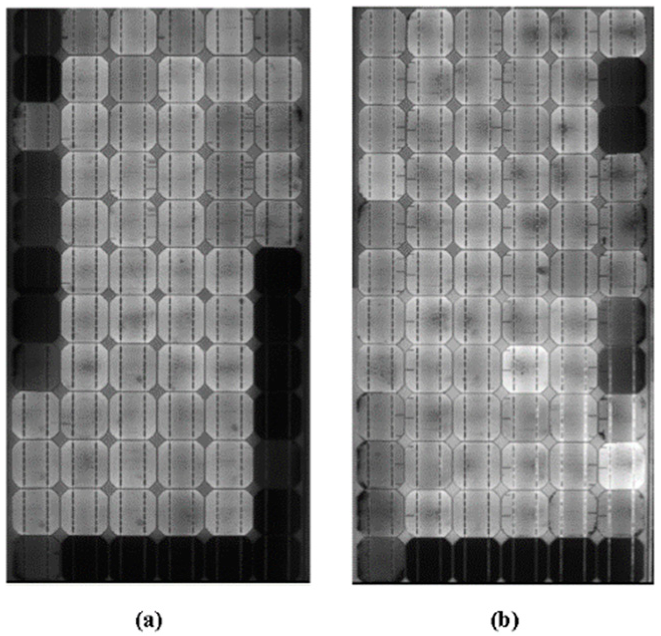
3.3. Hot Spot Heating

When a small crack appears in a PV cell during the manufacturing process or during transportation, it may have a very marginal effect on the performance of the cell. However, after installation, micro cracks can evolve into the physical breakage of cells. As a consequence, a current mismatch between the cells occurs. The damaged cells may have a much smaller short circuit current than the healthy cells, and the characteristic curve of the entire submodule can change [39,40,41]. For example, one submodule that has 20 series-connected cells, with two of the cells either damaged or under the shade, has a consequently lower ISC (or photo-generated current Iph). The I-V curve of the healthy PV cells in the forward region can be drawn using the single diode model [42,43,44], in which a single exponential and five parameters are involved in the cell behavior like a generator (both voltage and current are positive). As shown in reference [45], more advanced models can be used to simulate the behavior of solar cells in reverse bias in order to study the partial shading effect.
Figure 6 shows the I-V curve of the shaded and irradiated cells. In this figure, the curve of the entire 20 cells is also given. This net I-V curve has a non-zero slope in the current source region due to a relatively low shunt resistance Rsh of the partially shaded cells. Similarly, the Iph is also decreased because of the current mismatch. The small Rsh represents the existence of a high conductivity shunt path across the cell p-n junction or on the cell edges. These shunt paths lead the current away from the intended path and affect the performance of the module, particularly at low intensity levels [46,47]. If the dissipated power goes beyond a certain value, hotspots may occur on the PV cells, making their failure possible or possibly resulting in further consequences to the other components of the PV plant (e.g., fuses and wires), such as fires [48] and short circuits [49]. The magnitude of reduction in the shunt resistance depends upon various factors, such as the number of shaded cells or the level of irradiance.

3.4. Disconnected Cells and Faulty String-Ribbon Interconnection

The manufacturing process, named “tabber-stringer” [50], allows for the interconnection of individual solar cells in strings thanks to the use of ribbons. Every single cell is, in this way, soldered on the busbars to the back of the neighbor cell in order to create a series connection. This procedure induces high mechanical stress within the cells. If this stress is accompanied by poor soldering of the string interconnect ribbons, “latent cracks” not detectable during the manufacturing process are generated, and they are causes of future cell cracks or ribbon disconnections [51]. A single disconnected ribbon leads to an increase in the series resistance of a PV module that can cause power losses up to 35% [7]. In the past, two busbars were used, while today, more than three are used. As a consequence, in the past, if two ribbons of a cell were electrically disconnected, the current flowing through the string of cells would be immediately interrupted, and the bypass diode would be activated in order to protect the PV group of cells against this current mismatch. This action permitted the recovery of the entire current produced by the normal cells. In any case, the power generation of the cells with two busbars configuration is definitively compromised.
PV module failures can be detected by IRT and EL imaging. However, the I-V curve can also identify this problem easily via observing the increase in series resistance and decrease of FF. It is found in reference [52] that, with a 0.1 Ω increase in the value of the series resistance, the FF decreases by about 2.5%. Similarly, the conduction of bypass diode at lower values of current can also indicate the possible existence of this type of fault. Figure 7 shows the characteristic curves of a typical 20 cell PV submodule with different values of series resistance. From this figure, we can note how the increase of Rs affects the FF.

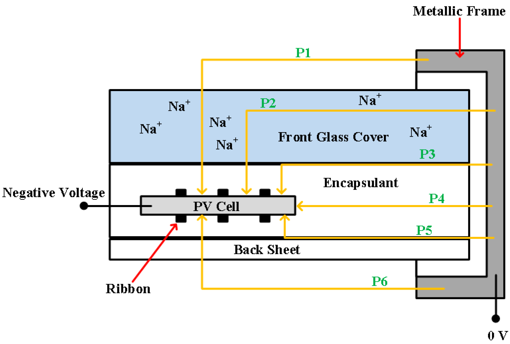
3.5. Potential Induced Degradation

Potential induced degradation (PID) is one of the defects that has gained the attention of PV experts in recent years. In order to increase the voltage of the PV generators, the modules are connected in series to form PV strings. The voltages of the strings can reach up 1500 V in grid-connected plants. The frames of the modules are mechanically connected to ground for safety. In centralized inverter and string inverter systems, a high voltage gradient develops, between the PV cells and the module frame, which leads to the appearance of PID. Figure 8 shows a PV string in which the modules are connected in series in order to increase the system voltage [52]. For the sake of simplicity, the example shows five series-connected modules. In Figure 7, the potential difference between module 3 and its frame is negligible. In modules 4 and 5, the voltage gradient between the cells and the frames increases positively, leading the current from the PV cells to the frame of the modules. Likewise, in case of modules 1 and 2, the voltage of the frames is higher than in the cells and the leakage current flows from the frame to the cells [53].
Figure 9 can be used as an example of modeling the leakage current leading to PID [53,54]. In this figure, the PV cell is negatively biased with respect to the frame of the module. The leakage current, flowing through different paths marked in yellow arrows, is described as follows:
  • In path P1, the current flows along the surface of the glass cover and via the bulk of the glass and the encapsulant;
  • Through path P2, the current flows through the bulk of the glass cover and that of the encapsulant;
  • From the frame along the junction of the front glass cover and through the encapsulant (path P3);
  • From the frame through the encapsulant towards the negatively biased PV cell, shown as P4;
  • Along the interface of the encapsulant and the backsheet and through the encapsulant (P5); and
  • In P6, the leakage current flows from the frame along the backsheet and through it and the encapsulant.
Figure 9 shows the leakage current paths for a negatively biased PV cell. When the cell is positively biased, the direction of the current paths is reversed. The degradation due to PID under the negative biasing of the PV cells is more severe as compared to the losses and degradation under the positive bias of the cells [55,56].
PID particularly results in the formation of cell shunts (in the case of negatively biased PV cells), and its effect can be seen through reduced shunt resistance, as well as lower open circuit voltage and low FF. It is concluded by the authors of reference [57] that, in the initial stages, the degradation in performance of a PV module from PID is small at higher irradiance levels and greater under the low illumination conditions. In some cases, PID is reversible, and recovery can be obtained by the application of reverse voltage to the glass frame at a high temperature [8].
Figure 10a,b gives the EL images of two mono-crystalline Si PV modules affected by PID. The cells affected by PID can be identified from their darker colors. Obviously, the PID first affects the cells near to the frames. Then, if the modules with this defect are subject to high system voltage for extended periods of time, the inner cells are also affected. Figure 11 shows the I-V curve of the affected module of Figure 10a. The PID-affected modules have lower VOC, voltage at maximum power VMPP, and reduced FF.

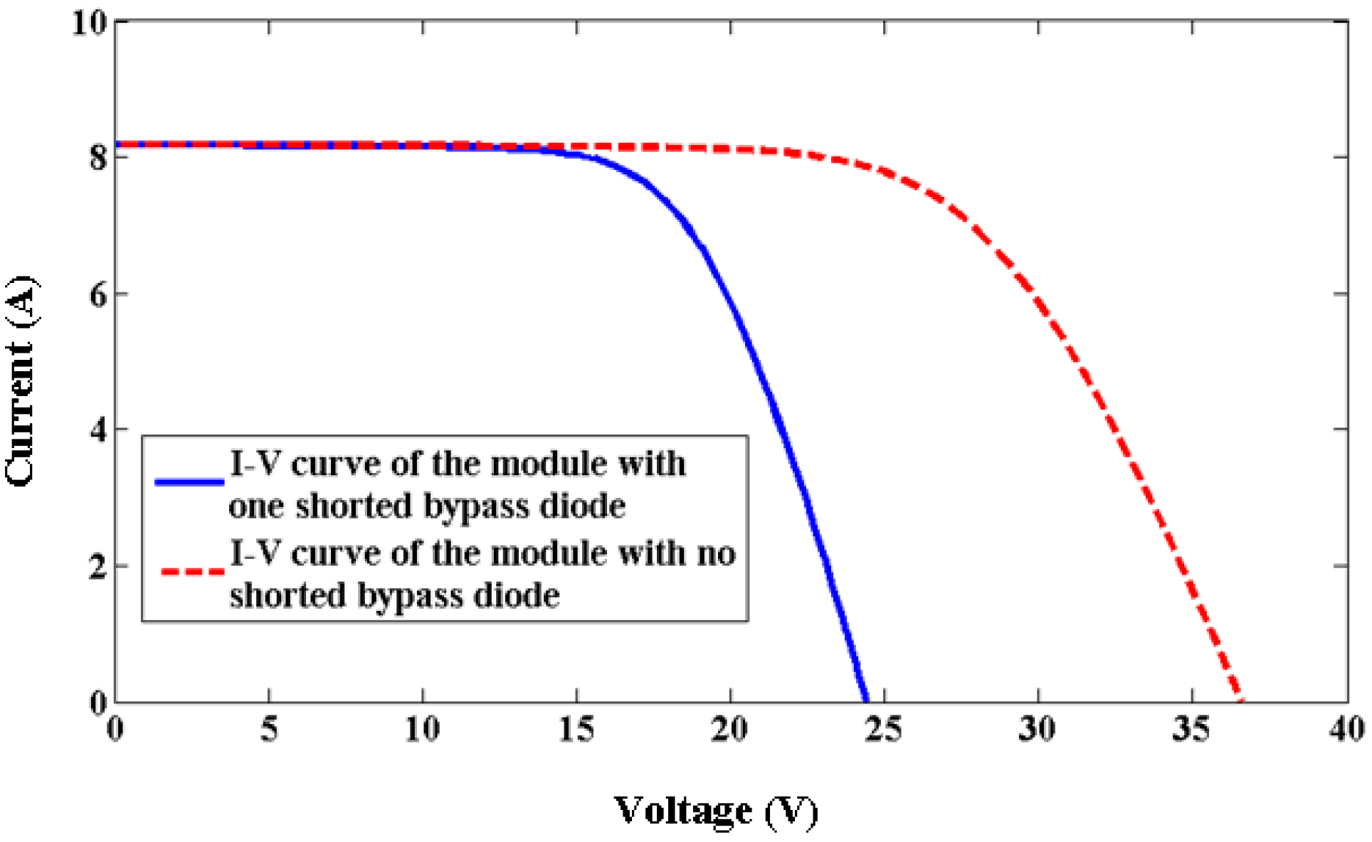
3.6. Defective Bypass Diodes

Bypass diodes are installed in the PV modules in order to protect PV cells against the current mismatch result of shading and other internal defects. In installing the bypass diodes in the modules, the magnitude of breakdown voltage of a single cell is considered [58]; thus, a diode is generally installed for a group of about 20–24 cells. One of the main defects of the bypass diodes is the short circuit fault. A short-circuited diode can be immediately detected from the reduction in power of the PV modules. If each PV module is equipped with three bypass diodes, the underperformance is usually 1/3 of the maximum power and 1/3 of open circuit voltage (Figure 12). An open-circuited diode has no effect on the operation of an unshaded PV module. In the event of shading, a module with open-circuited diode can be subject to high reverse voltage. Such a PV module is highly susceptible to damage and is even a fire hazard in the case of overheating [59].
Regarding the failure rate of bypass diodes, it is reported in reference [60] that during the inspection of an eight-year-old PV plant in Japan, out of 1272 modules, 47% showed diode failures. In another study, 26 out of 2352 modules showed diode failures in Arizona, USA [61]. Besides the power reduction of the modules, the diode failures also can lead to follow-up faults of the PV cells. It is therefore important to mention the reasons for diode failures. Some of the important factors for the damaging of bypass diode in PV modules are [62]
  • When a PV module of a string is shaded (or a few cells of a single module), the bypassed diodes of the shaded module start to conduct (partial shading). Due to conduction of current, their temperature increases and can easily exceed the maximum temperature for the materials of the PV modules (≈ 85 °C). The regular operation of the bypass diodes causes spot heating in the PV modules [63].
  • Bypass diodes undergo thermal runaway in the event of cyclic transition from forward to reverse bias [64]. This thermal runaway takes place when the power dissipation in the reverse biased diode is greater than the cooling capacity of the junction box.
  • Shading and fluctuations in irradiance can also lead to regular current cycling via the bypass diodes. Self-heating leads to thermal cycling.

4. Finding the Values of Parameters for Fault Diagnosis from On-Site Measurements

As described in Section 2.2, abnormal variations in VOC, ISC, Rs, and Rsh, obtained after the characterization of the I-V curve, suggest different types of defects of the PV modules. The estimation of VOC and ISC of a PV module from onsite measurements is relatively easy; however, the calculation of accurate values of Rs and Rsh from onsite measurements is challenging.
For this reason, in this section, different methods proposed in the literature are discussed which find the values of the parasitic resistances. These methods permit the identification of a defect in a poly-crystalline PV module. These methods are also valid for mono-crystalline silicon and thin film modules, as written in reference [65]. Among the parameters previously listed in Section 2.2, parasitic resistances can give information about the state of health of PV modules under operation, and a rapid diagnosis of faults allows a fast maintenance and permits the reduction of energy losses. For example, one of the reasons for the decrease of shunt resistance of the modules is the accumulation of dirt on the surface of the modules. If the layer of dirt is not discovered in time, the operation of the dirty module may result in the formation of hotspots. These hotspots represent permanent damage to the PV modules. Likewise, the decreased shunt resistance also gives an indication of broken cells. Similarly, an increased series resistance gives the indication of a broken cell interconnection.
For improving the performance of PV plants, online monitoring and diagnosis have become a necessary feature of PV generation plants [66,67,68,69,70,71]. Recently, various manufacturers have developed tools for visualizing the performance of PV arrays [67]. For example, the inverter in [67] can obtain data about the energy generated from the PV plant in certain time intervals, the cumulative energy production, etc. This information can be acquired from the inverter for further analysis related to the state of health of the plant. Monitoring of the plants can be further improved if a scheme is developed for finding the other parameters, like the parasitic resistances of the modules, their short circuit currents, and open circuit voltages. Similarly, prototype devices have been proposed in references [68,69] that can report the performance of PV modules under the field condition. To make these devices more useful, the inclusion of information about the parasitic resistances is of great value.

4.1. Current Methodologies for Determination of Shunt and Series Resistances

Regarding the determination of shunt resistance Rsh, references [69,70,71] report methods for computing this value. In reference [70], the shunt resistance of the module is found from the characteristic equation of the single diode model, i.e.,
I = I p h I 0 ( e x p ( V + I R s n s a V t ) 1 )   V + I R s R s h .
At the short circuit point I = ISC and V = 0, the above equation becomes
I S C = I p h I 0 ( e x p ( I S C R s n s a V t ) 1 )   I S C R s R s h .
By taking the derivative of Equation (2) and after some simplifications the result is
R s h R s h 0 .
where Rsh0 represents the segment between points B and C, as shown in Figure 13. The method proposed in reference [70] is useful only when the PV module operates under the conditions close to STC. When the temperature of PV cells becomes high, the approximation of Rsh as the slope of the I-V curve, according to Equation (3), does not return an accurate value of the shunt resistance. This fact will be made clear in the simulation results.
Regarding the determination of series resistance Rs, several methods are reported in literature. The first method discussed here is the one given in [72]. This technique measures the degradation in the PV-module performance through series resistance estimation. This scheme is based upon the single diode model with the characteristic equation given in Equation (1). The other important quantities are calculated in the following equations, where the subscript n stands for nominal conditions—that is, standard test condition (STC): Gn = 1000 W/m2, Tn = 25 °C, according to references [43,73,74,75].
I p h =   ( I s c n + K I Δ T ) G G n
I 0 =   I s c n + K I   Δ T   e x p ( ( V o c n + K V   Δ T ) / a V t ) 1
R s = R s ,   n T T n ( 1 0.217   l n ( G G n ) )
According to Equation (6), the temperature and the effective irradiance are needed. Due to the discoloration of the EVA and soiling of the surface of a module, it is difficult to calculate the effective irradiance over the module. For this purpose, some approximation of the effective irradiance is required. The effective irradiance G can be calculated as follows:
I p h = I S C
G =   G n I S C I S C ,   n   +   K I Δ T .
The temperature of the module is calculated from the Ta as
T = T a + ( N O C T 20 ° C 800 W / m 2 ) G ,
where NOCT is the normal operating cell temperature provided by the manufacturer of the PV modules.
In this method [72], the reduction in the value of VMPP is considered as an outcome of the additional series resistance. In the first step, VMPP and IMPP of the module are measured. In the second step the reduction of VMPP is computed as
Δ V M P P = V M P P ,     i d e a l     V M P P ,   r e a l .
The increase in Rs is considered to be brought about by an increase in the series resistance ΔRs calculated as
Δ R s =   Δ V M P P I M P P .
The additional series resistance is normalized with respect to the model parameter as
N Δ R s =   Δ R s R s .
In the above method, any degradation is translated in the form of increment in the module Rs. However, it is important to note that many degradations like ageing, corrosion of the metal semiconductor interface, and PID cause a reduction in VMPP. Similarly, a decreased Rsh also causes a reduction in VMPP. The method proposed in reference [72] manifests these defects as a “fictitious increase” in Rs. This means that the actual value of the Rs cannot be found by means of this procedure.
In [76] another method to find Rs is proposed. In this scheme the derivative of voltage with respect to current is calculated at point nearby IMPP. As described in reference [72], the performance degradation of a PV module is detected by monitoring the changes in PV generator’s series resistance. In this way, the information about the variation of Rs is also obtained along with finding the MPP. The knowledge of the short circuit current is needed and the same ISC is found from IMPP by the relation ISC = IMPP/fI. Here, the value of the factor fI is approximately equal to 0.92, because the manufacturers of PV modules declare IMPP and ISC corresponding to a ratio in the range 0.90–0.95. The optimal point at which the derivative of voltage with respect to current is evaluated is denoted by Q. There are two options for choosing Q:
Q = I S C 0.75 I M P P
or
Q = I S C 0.60 I M P P .
The final expression to find Rs is
R s =     d V d I | I   =   Q =     V 2       V 1 I 2       I 1 .
The evaluation of Rs from Equation (15) requires the measurements at two points (I1, V1) and (I2, V2) close to point Q.
The novelty of reference [76] is that it has combined the diagnosis of a PV module with MPP tracking. However, the shortcoming of this scheme is that, for more comprehensive diagnostics information, the value of Rsh is also necessary. Similarly, the estimation of ISC from IMPP becomes inaccurate under the circumstances when the shunt resistance of the module decreases.
A more conventional method involves the evaluation of the derivative of voltage close to VOC [7,76], i.e.:
R s 0   =       d V d I | V   V O C =     V 2 V 1 I 2 I 1 | V = V O C .
According to reference [7], it is equal to the estimated value of the series resistance of a module. However, the value of the series resistance estimated from Equation (16) varies with changes in irradiance and temperature. The authors of reference [77] propose an improvement of the method by taking into consideration the irradiance and temperature. The modified relation is given as
R s = R s 0 +   V t I S C   ( G G n   .   T n T 1 ) .
Reference [71] makes use of RS0 for calculating the series resistance through the following equation:
R s = R s 0   1 I 0     a k T q   e x p ( V O C n V t ) .
Equation (18) can be used to calculate the value of the series resistance. However, for this purpose, the accurate value of the VOC is required. It means that the PV generator has to be disconnected from the load. Frequent disconnection of the PV generator from the load not only results in power loss but can also create power quality issues in grid-connected PV plants.

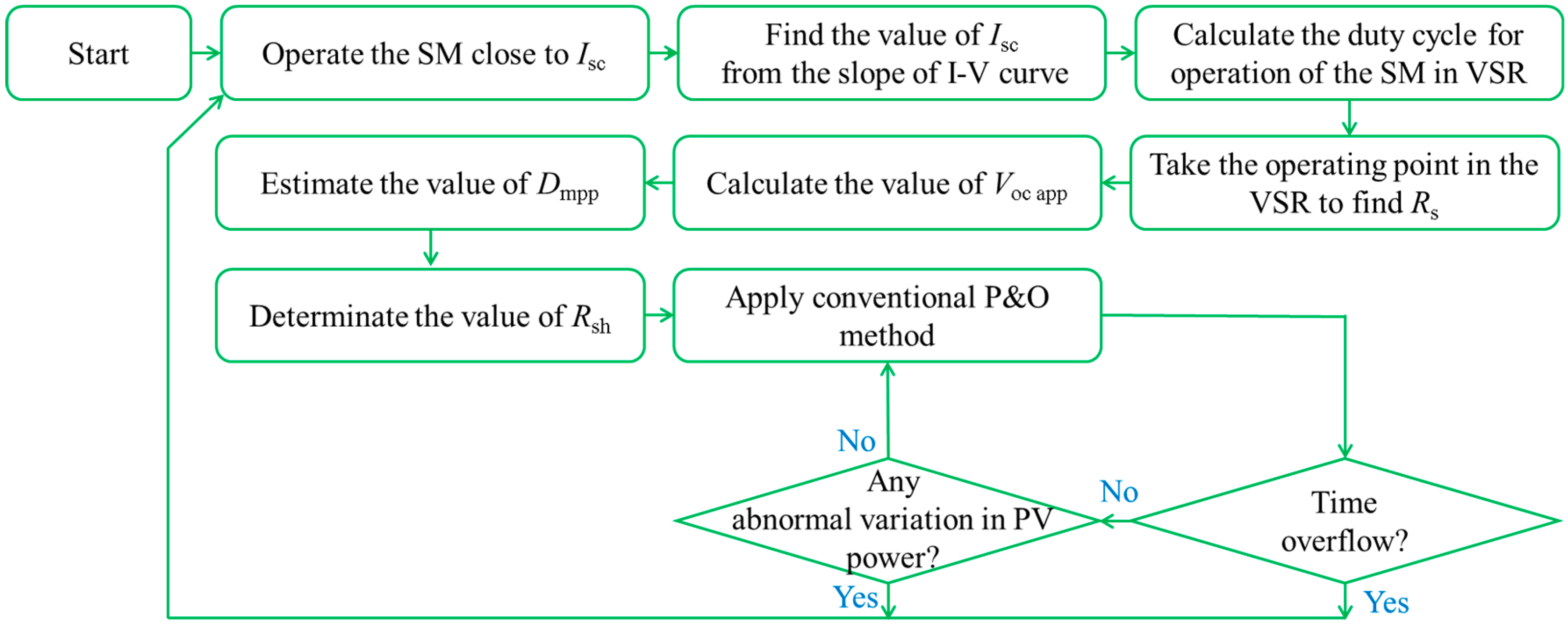
4.2. The proposed Alternative Methodology for the Determination of Shunt and Series Resistances

In Section 4.1, some methods to find the parasitic resistances of PV modules is presented. The limitations of these methods have also been discussed. In this subsection, a different method is proposed to find the shunt and the series resistances. This method will be applied in Section 5.
Figure 13 shows the I-V curve of a PV module with uniform irradiance. Consider a point A on the curve. This point is in the voltage source region of the characteristic curve. The equation that relates the current (IA) and voltage (VA) at point A from the single diode model is
I A = I p h I 0 [ e x p ( V A + I A R s a V t ) 1 ]   V A + I A R s R s h .
From the slope of segment BC in Figure 13, the value of ISC or Iph can be extrapolated. Similarly, from the slope of segment between A and E points, the value of the open circuit voltage can be extrapolated. Once the values of Iph and Rsh, Vt and I0 are known, the above equation can then be solved numerically to find Rs. One of the well-known numerical algorithm is the Newton-Raphson (NR) method. The NR algorithm can be easily implemented through a computer program. However, when it is desired to calculate the value of series resistance under real time operation in the field, a powerful microcontroller may be required for implementing the NR method for solving the Equation (19) numerically. For reducing the computational burden on the microcontroller, the Equation (19) must be expressed in an explicit form. According to [78], the influence of Rs is stronger in the voltage source region, while that of Rsh is stronger in the current source of the PV electrical curve. According to Figure 13, point A is in the voltage source region of the PV generator. Therefore, in Equation (19) the term involving Rsh is neglected:
I A = I p h I 0 [ e x p ( V A + I A R s a V t ) 1 ]
Solving this equation for Rs, the results is:
R s =   a V t I A ln ( I p h I A I 0 )   V A I A
Finding the value of series resistance from Equation (21) involves the operation of a PV module at a single point in the voltage source region of the I-V curve, for example, at point A in Figure 13. When the module is operated at point A, the corresponding values of voltage VA and current IA are then used in Equation (21). The value of saturation current I0 is dependent on the temperature which is taken from temperature sensor [72] and then Equation (5) is used to calculate the saturation current. Thermal voltage Vt is also temperature dependent. Thermal voltage is determined as V t = n s k T / q   where ns is the number of series connected cells in the module, k is Boltzmann’s constant, T is the temperature, and q is the electron charge. Thus, through the use of Equation (21) one can easily estimate Rs.
Regarding the determination of Rsh, the characteristic equation Equation (1) is solved assuming that the PV module operates at the MPP, where the value of RS is calculated according to Equation (21).
I M P P = I p h I 0 ( e x p ( V M P P + I R s n s a V t ) 1 )   V M P P + I R s R s h
For the sake of clarity, the determination of the needed parameters to for defect diagnosis is summarized as follows:
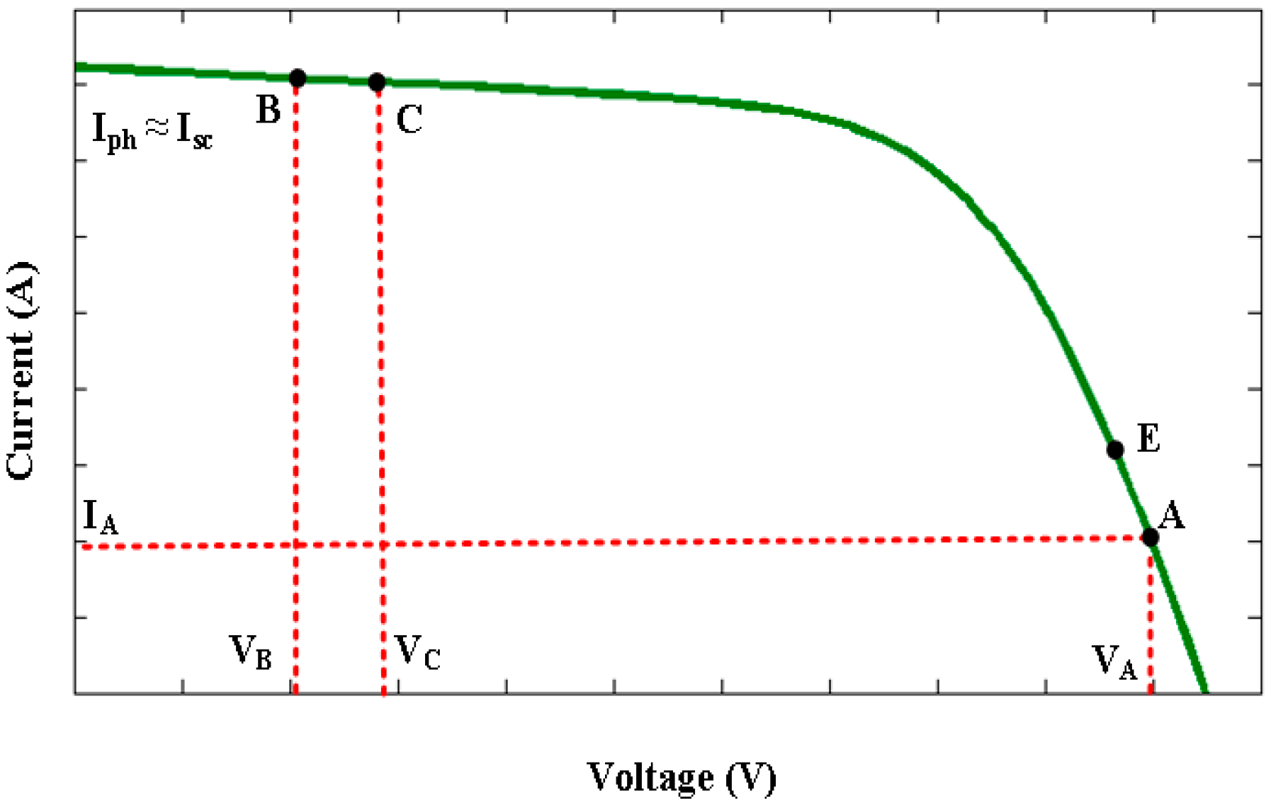
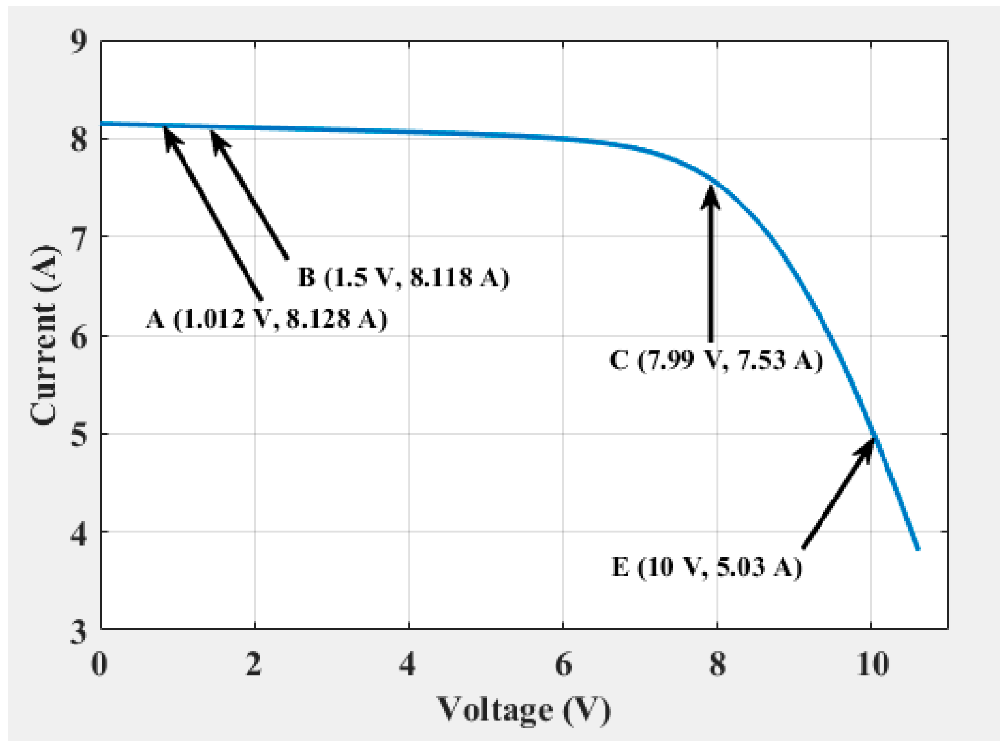
  • Take the operating point of the PV generator close to ISC. From the slope of the I-V curve close to ISC, estimate the value of ISC (or Iph).
  • Take the operating point of the PV generator close to VOC and estimate the value VOC from the slope of the I-V curve (for example points A and E in Figure 13).
  • Calculate the value of Rs by using Equation (21)
  • Operate the PV generator at the MPP (or close to it) and use Equation (22) to find the value of Rsh.

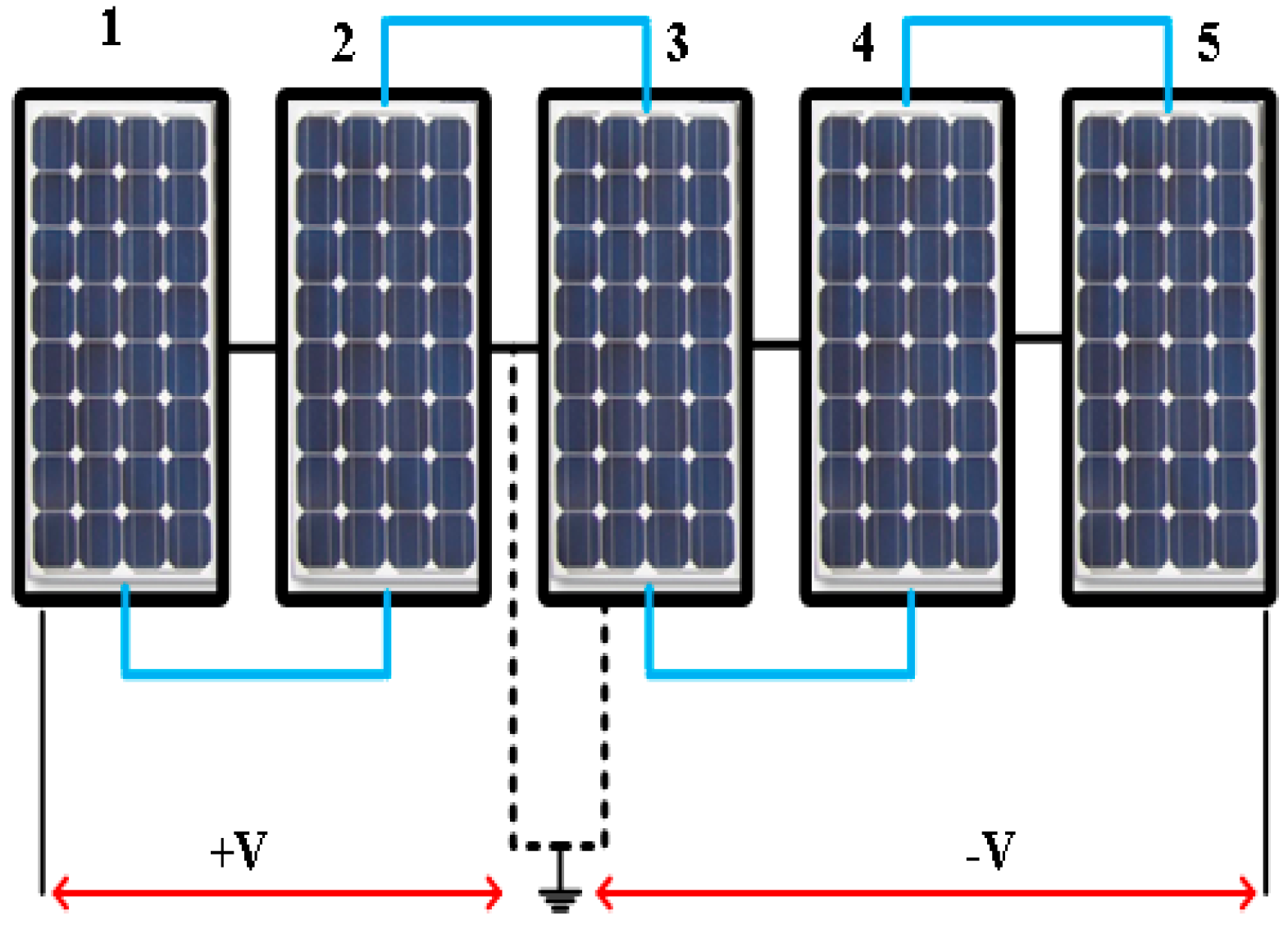
5. Maximum Power Point Tracking for Fault Diagnosis

5.1. Comparison of Maximum Power Point Tracking Architectures

Different types of Maximum Power Point Tracking (MPPT) architectures are used for the taking out maximum power from PV arrays under given environmental conditions. From an historic point of view, these architectures include [79]:
  • Centralized MPPT architecture (the oldest one).
  • String inverter scheme.
  • Module integrated MPPT scheme.
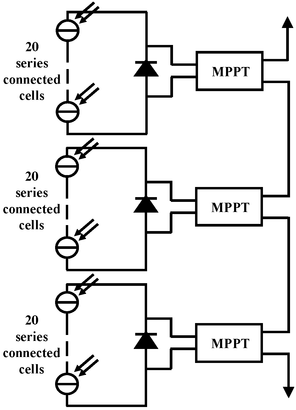
  • SubModule Integrated (SMI) MPPTs (the newest one).
The centralized MPPT architecture is the simplest, and the MPP tracking is performed on the entire array. The drawback of this arrangement is that the power losses in case of the modules mismatching and partial shading are high. Similarly, the fault diagnosis during the normal operation is extremely difficult. To reduce the mismatch losses, string inverter architecture is one of the best solutions. In this architecture, the MPP tracking for each string is performed and the mismatch losses are lower than in case of centralized architecture. When the system voltages are higher, the modules are prone to PID in the central and string inverter MPPTs. In order to further decrease the mismatching loss, module and submodule integrated (SMI) MPPTs have been proposed in literature [79,80,81,82,83]. The architecture of SMI MPPT is shown in Figure 14. Usually, in a PV module 20 or 24 PV cells are protected by a single bypass diode. In case of SMI MPPTs, every submodule (a group of cells protected by the same bypass diode) has its own MPPT. The SMI MPPTs most important advantages are listed below:
  • The SMI MPPT architecture decouples module from PV strings and in this way, the MPP control of each SubModule (SM) is possible.
  • Online monitoring and diagnosis of the PV modules is easy. As shown later in this paper, it is possible to check the existence of a fault by making small adjustment in the MPPT algorithm.
  • Some inverters are able to communicate with the PV modules by exchanging the performance data [67]. In this way, the extent and the physical location of a fault is easily known.
  • In reference [84] it is predicted that, during the 30 years of operation, the SMI architecture yields more power in different installations like PV plants on land, rooftop, façade, and electric vehicles. In references [85,86], it is reported that this configuration gives 20% more energy as compared to other types of DMPPTs.
  • The hardware for DMPPTs can be installed in the junction box of the PV module and a single microcontroller performs the MPP tracking of all the three submodules [85]. Even though the arrangement in [80] does not use a current sensor and measures the voltage drop across the inductor of the buck converter for estimating the current, it is possible to use an accurate Hall Effect based current sensor for accurate measurements. The cost of these sensors has decreased in recent years and accurate sensing of current is possible without any substantial increase in the system cost.
  • In references [76,77,78,79,80], researches investigate the possibility of avoiding the installation of bypass and the reverse blocking diodes. According to [87], the insertion of the blocking diodes against reverse currents can be avoided with crystalline silicon technology, provided that the short circuit fault inside the submodule is not possible thanks to the double insulation typical of commercial PV devices.
  • The PV modules in the string and centralized inverter schemes are subject to high voltage stresses which make them vulnerable to PIDs. In the SMI MPPTs, every submodule operates independently at a voltage less than 20 V. This eliminates the risk of PIDs.
  • The MPP tracking is quite easy as there is always a single peak on the P-V curve of the SM. In this way, a conventional MPPT scheme can be used to track the peak. Through small modification in the algorithm, it is also possible to improve the tracking speed of the conventional MPPT and to obtain the diagnostics information.

5.2. Application of Submodule Integrated MPPT with Fault Diagnosis

In this subsection, a MPPT scheme is proposed which has additional features of extracting information about the possible existence of a defect in a PV submodule. This method is applicable for the sub-module MPPTs. The proposed algorithm not only finds the MPP, but it can also estimate the values of Rs, Rsh, VOC, and Iph of each sub-module.
Before explaining the proposed algorithm, it is necessary to discuss the procedure that is followed for operating a PV generator in a certain point on the I-V curve. This is done by setting the duty cycle of the DC-DC converter to an appropriate value. Let us consider the case of a buck converter. As an assumption, the converter is operating in a certain point with duty cycle D1 = Vout1/Vin1. The output side of the DC-DC converter, regulated at constant voltage, supplies a load, which could be directly a DC load or the input side of a centralized voltage source inverter. Hence, the selected value of duty cycle is inversely proportional to the imposed input voltage Vin. The voltage and current at the input of the converter are Vin1 and Iin1, respectively. In order to operate the PV in a certain point with voltage Vin2 and current Iin2, the new duty cycle D2 is calculated as
D 2 =   R o u t I i n 2 V i n 2 ,
where Rout is the output load resistance, i.e., Vout2/Iout2. Considering the analysis in references [86,87,88], Rout is calculated as follows
R o u t = D 1 2 V i n 1 I i n 1 .
The flowchart given in Figure 15 describes the proposed method. At the beginning, the algorithm operates the SM close to the ISC. At this stage the duty cycle of the converter is changed slightly to shift the operating point to the higher voltage side, i.e., from point B to C in Figure 13. This is done for the purpose of calculating the slope of the I-V curve in the neighborhood of ISC and estimating the value of Iph. Then, Equation (3) is used to find the Rsh of the SM. The next step is to take the operating point of the system to the Voltage Source Region (VSR) of the SM, as shown by block 5 in Figure 15.
For this purpose, it is necessary to find Rout. The operation of the PV is still in the current source region assuming that it has voltage V1 and current I1, and using Equation (24), Rout is calculated. The next step is to find the values of I2 and V2 in Equation (23). For this purpose, the current of the SM is approximated equal to the half of its photo-generated current, V2 is approximated to be 90% of the rated VOC of the SM. These values are inserted in Equation (23) to determine the value of duty cycle D2 of the converter for taking the operation to the VSR of the SM. By setting the duty cycle of the converter equal to D2, the operation is taken to the VSR, for example to point A in Figure 13. As shown in block 5 of the flowchart in Figure 15, the value of Rs of the SM is calculated using Equation (22). Then the duty cycle of the converter is slightly increased to take the operating point to E in Figure 13. From the slope of the segment AE the value of VOC of the SM is approximated and it is denoted as VOC,app. This is done for estimating the MPP voltage of the SM. The duty cycle of the converter corresponding to MPP is denoted as DMPP and is found by using Equation (23). In this case, it is necessary to replace I2 and V2 with IMPP and VMPP, where
I M P P = 0.92 ( I p h   V O C ,     a p p R s h ) ,
V M P P = 0.8   V O C , a p p .
By setting the converter’s duty cycle equal to DMPP, the operating point of the system is taken to MPP. After taking the operating point of the SM close to the MPP, Rsh of the SM is calculated using Equation (22). Then, the algorithm invokes a low cost P&O procedure to operate the system at the MPP in the steady-state. In the steady-state operation, the value of the perturbation step is kept small to reduce the oscillations around the MPP. The P&O algorithm maintains the operation at the MPP for minor changes in the irradiance conditions. During the operation of the P&O algorithm the PV output power is monitored for any abnormal variation. As shown in block 10, if the change in the output power of the PV during a certain sampling period is greater than the recorded MPP power, the whole process revealed in Figure 15 is repeated. As a conclusion, this process is a loop in which the P&O works continuously. In case of an abnormal variation of power, or after a predefined time overflow (several tens of seconds up to few minutes), the MPPT tracking with the determination of the equivalent circuit parameters is performed; then, the traditional P&O restarts.
The algorithm presented above has been simulated in MATLAB/SIMULINK. The PV generator used in the simulations is a typical 20 cell SM with rated VOC = 12.2 V and ISC = 8.2 A under STC. The simulated I-V curve of the PV generator under STC is shown in Figure 16.
This figure also shows various points on the characteristic curve along with their coordinates. For example, point A corresponds to 1.012 V and 8.128 A. Starting from Equation (3) [73,74], it is possible to calculate the shunt resistance that turns out to be Rsh = 48.8 Ω, which is an approximated value. Similarly, using Equation (22) and the coordinates of point E in Figure 16, the series resistance is Rs = 0.3026 Ω. As will be shown in the simulations, the method of slope of the characteristic curve in the proximity of ISC (given in [70,71]) gives inaccurate value of Rsh when the temperature is high. To overcome this problem, the proposed algorithm will take the operating point of the SM close to the MPP (corresponding to point C in Figure 16). Using the current (IC) and voltage (VC) at point C and taking ISCIph, Equation (3) can be written as
I C = I S C I 0 ( e x p ( V C + I C R s n s a V t ) 1 )   V C + I C R s R s h .
Solving the above equation for Rsh gives the value Rsh = 47.95 Ω. This algorithm is simulated for two cases:
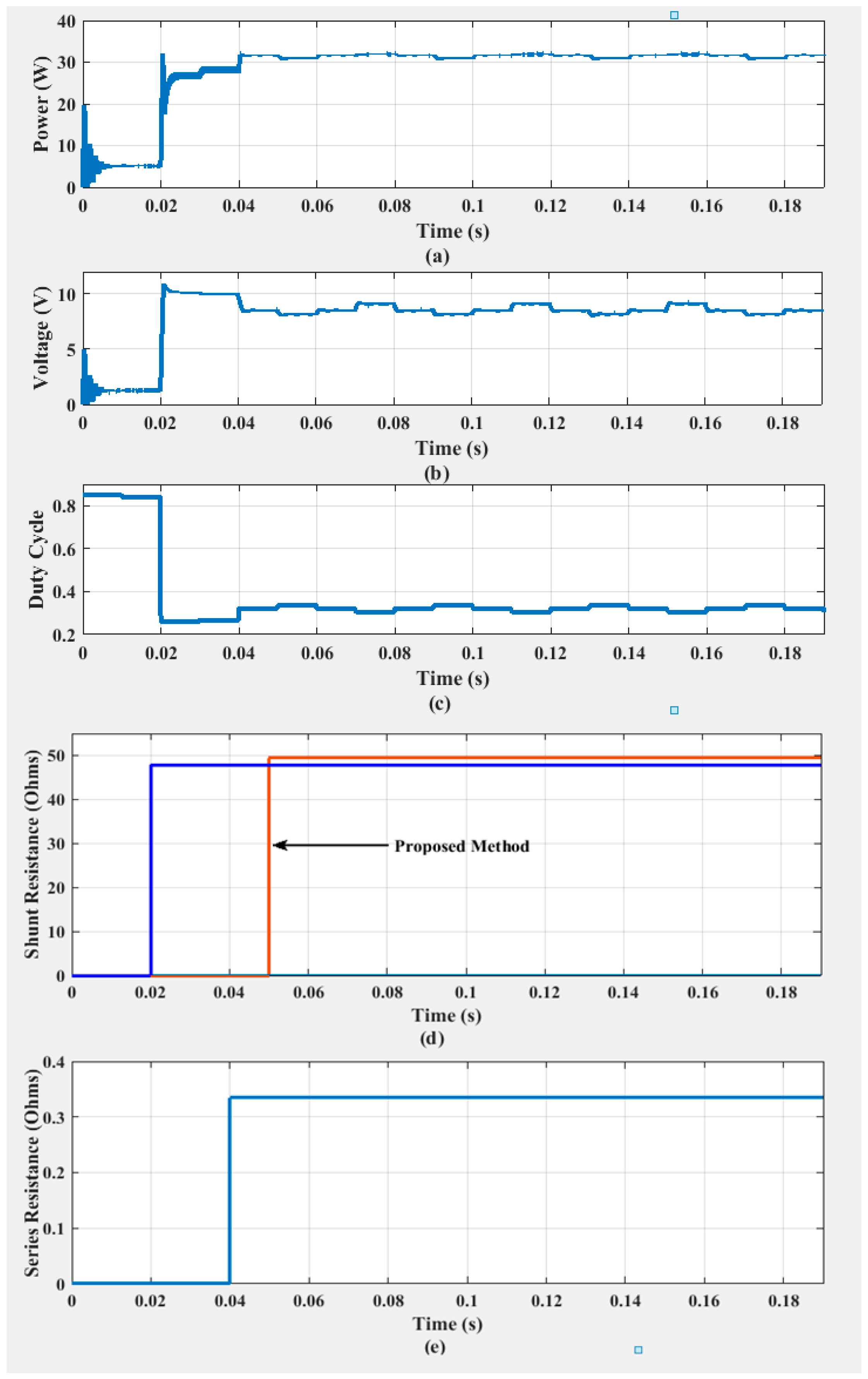
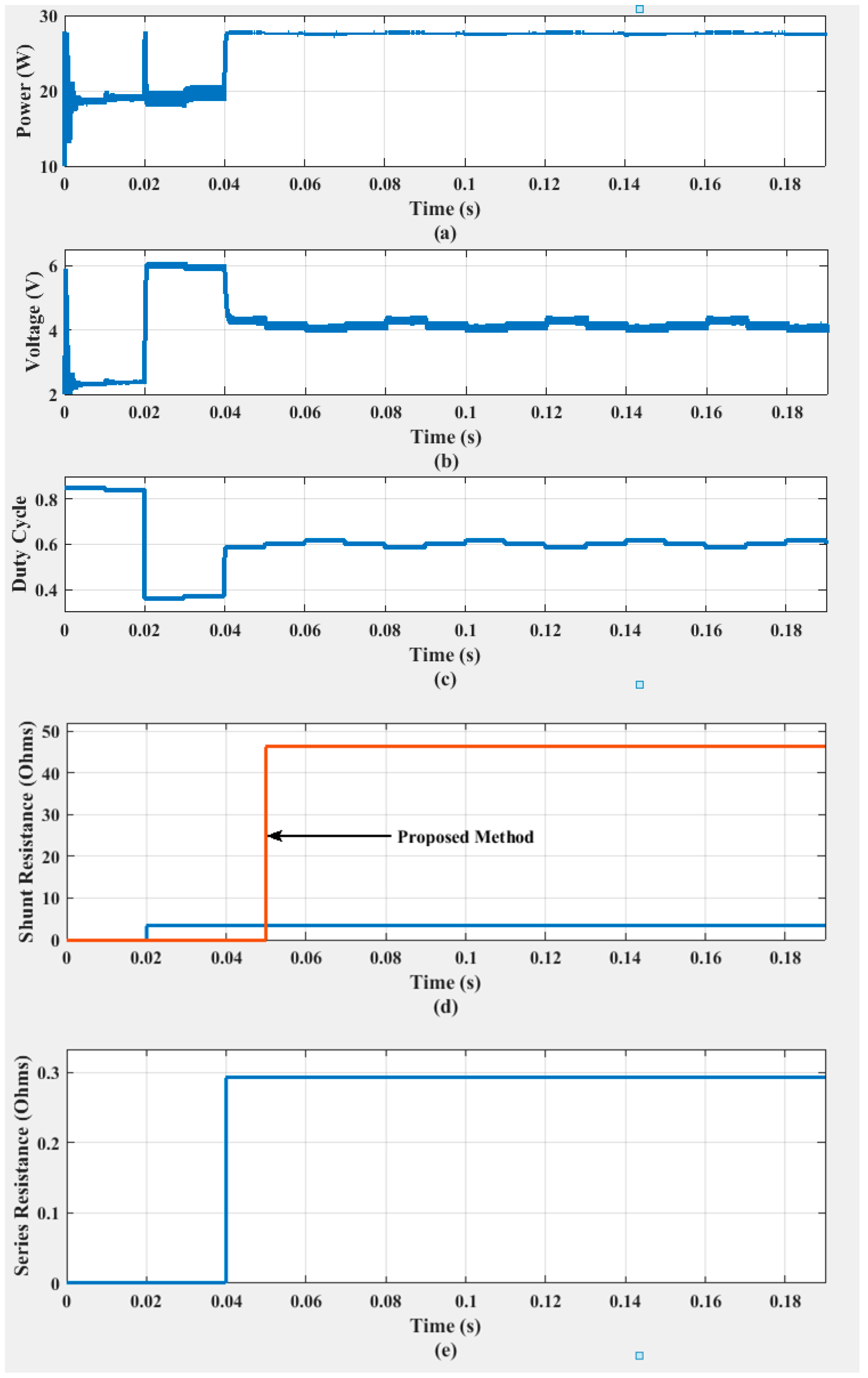
  • When irradiance G = 500 W/m2, and cell temperature T = 298 K;
  • When G = 700 W/m2 and T = 348 K.
The SM is connected to a DC-DC buck converter with switching frequency of 100 kHz and the sampling period is taken as 10 ms.
Figure 17 shows the simulation results when G = 500 W/m2 and T = 298 K. At the start of the algorithm, the PV source is operated close to ISC.
At t = 0.01 s, duty cycle of the DC-DC converter is slightly reduced to take the operating point to the right for estimating the value of ISC. At this stage, Rsh is found by using Equation (3), which is 47.9 Ω, as given in Figure 17d. Then the operating point of the SM is taken to VSR. This is done to find Rs using Equation (22) and VOC, app. The value of Rs is found to be 0.33 Ω, as shown in Figure 17e. At t = 0.05 s (given in Figure 17d) the value of the shunt resistance is calculated Rsh = 49.4 Ω. This is calculated by solving the current-voltage equation of the PV source for the values at that point (similar to Equation (27)). The value of shunt resistance, determined from the proposed method and the one found from Equation (3) [70,71], does not differ much from each other in this case, but the difference of the two methods increases when the temperature of the SM is higher. Similarly, the value of the series resistance is also close to the one found for the SM under STC. As shown in Figure 17, from t = 0.05s, the algorithm invokes conventional P&O algorithm to maintain the operation of SM around the MPP in the steady state, as indicated by block 9 of Figure 15.
However, under the steady state, if there is an abnormal variation in the output power of the SM, it indicates a change either in the atmospheric conditions or the condition of PV SM. In case of this change, new MPP search operation begins, and at the end of the process, the new values of parasitic resistances and other parameters of the PV SM are calculated.
Figure 18 shows the simulation results for a second case study with G = 700 W/m2 and T = 348 K. By following the aforementioned procedure, the algorithm determines the values of parasitic resistances. The values of shunt resistance found by using Equation (3), which is proposed in references [70,71] is 3.31 Ω (shown in Figure 18d), while the value calculated by the proposed technique is 46.37 Ω. The shunt resistance found by the proposed technique is closer to that at the STC. On the other hand, the technique given in references [70,71] gives an inaccurate value of the shunt resistance. As given in Figure 18e, the value of series resistance using Equation (22) (which is the proposed method) measures 0.2935 Ω. The main drawback of the method given in references [7,76] is that the actual value of the series resistance cannot be calculated when the temperature changes. However, the proposed method calculates the value of series resistance of the SM, which is close to the one at the STC.
The simulation results show how to perform diagnostics of the PV sub-module during the MPP tracking. The techniques proposed in this paper to find the parasitic resistances are accurate as compared to the methods proposed in the literature. The values of the parasitic resistances, ISC, and approximate values of the open circuit voltage (VOC,app) found during the execution of the MPPT algorithm are communicated to the centralized inverter equipped with microprocessor and software able to detect occurred faults of PV modules and send messages to the users for addressing the issues [67,72]. These values can then be utilized to assess the existence of a fault in the SM.

6. Conclusions

In the present work, a review of defects, observed during the operational lifetime of PV modules, has been presented. The main objective of the review is to study the effects of these defects on the parameters of the equivalent of the PV modules, like the open circuit voltage, short circuit current, series resistance, and shunt resistance. The common fault diagnostic techniques, like electroluminescence and thermographic imaging, and their drawbacks have been discussed. The alternative to the aforementioned diagnostic tests is to determine the parameters of the equivalent circuit during the on-site operation of PV generators. With respect to current literature on this topic, a simple method to detect the values of the series and shunt resistances in the equivalent circuit of the PV generators has been proposed. Furthermore, it has been shown that MPPT tracking and defect detection by equivalent circuit parameters can be combined. This combination can be fruitfully applied in case of submodule integrated MPPT because no local maxima on the PV curve are present. Regarding the reference values for diagnosis purpose, simulation results, carried out at two irradiances and temperatures, demonstrate that a 20-cell polycrystalline silicon submodule, without intrinsic defects or shadows, exhibits a series resistance within 0.3–0.5 Ω and a shunt resistance within 40–50 Ω. This information is provided within 50 ms.

Author Contributions

J.A. carried out the original draft preparation and all the simulations. F.S. analyzed the data and results. A.C. and S.F. contributed to the paper writing and the whole revision process. All authors equally organized and refined the manuscript in the present form.

Funding

This research received no external funding.

Conflicts of Interest

The authors declare no conflict of interest.

Nomenclature

adiode ideality factor
IPV cell current (A)
Girradiance on the cell surface (W/m2)
Gnnominal irradiance (1000 W/m2)
IMPPmaximum power point current (A)
I0saturation current (A)
Iphphoto-generated current (A)
ISCshort circuit current (A)
Iscnnominal short circuit current (A)
kBoltzmann constant (J/K)
KIthermal coefficients of current (A/°C)
KVthermal coefficients of voltage (V/°C)
nsnumber of cells in series
NΔRsnormalized increase in the series resistance
qelectron charge (C)
Rsseries resistance (Ω)
Rs,nseries resistance of cells (Ω) under nominal conditions
RS0series resistance close to Voc (Ω)
Rshshunt resistance (Ω)
Rsh0negative reciprocal of the slope of the I-V curve close to ISC (Ω)
Ttemperature of the module (°C)
Taair temperature (°C)
Tnnominal temperature (°C)
VPV cell voltage (V)
VMPPmaximum power point voltage (V)
VOCopen circuit voltage (V)
VOCnnominal voltage (V)
Vtthermal voltage at STC temperature (≈25.7 mV)

References

  1. Rashid, K.; Safdarnejad, S.M.; Ellingwood, K.; Powell, K.M. Techno-economic evaluation of different hybridization schemes for a solar thermal/gas power plant. Energy 2019, 181, 91–106. [Google Scholar] [CrossRef]
  2. Rashid, K.; Safdarnejad, S.M.; Powell, K.M. Dynamic simulation, control, and performance evaluation of a synergistic solar and natural gas hybrid power plant. Energy Convers. Manag. 2019, 179, 270–285. [Google Scholar] [CrossRef]
  3. Renewables 2016 Global Status Report. Available online: https://www.ren21.net/reports/global-status-report/ (accessed on 28 November 2019).
  4. Mazza, A.; Chicco, G.; Bakirtzis, E.; Bakirtzis, A.; De Bonis, A.; Catalão, J.P.S. Power flow calculations for small distribution networks under time-dependent and uncertain input data. In Proceedings of the 2014 IEEE PES T&D Conference and Exposition, Chicago, IL, USA, 14–17 April 2014. [Google Scholar]
  5. Ciocia, A.; Boicea, A.V.; Chicco, G.; Di Leo, P.; Mazza, A.; Pons, E.; Spertino, F.; Hadj-Said, N. Voltage Control in Low-Voltage Grids Using Distributed Photovoltaic Converters and Centralized Devices. IEEE Trans. Ind. Appl. 2019, 55, 225–237. [Google Scholar] [CrossRef]
  6. Grimaccia, F.; Leva, S.; Dolara, A.; Aghaei, M. Survey on PV modules’ common faults after an O&M flight extensive campaign over different plants in Italy. IEEE J. Photovolt. 2017, 7, 810–816. [Google Scholar]
  7. Spertino, F.; Chiodo, E.; Ciocia, A.; Malgaroli, G.; Ratclif, A. Maintenance Activity, Reliability Analysis and Related Energy Losses in Five Operating Photovoltaic Plants. In Proceedings of the IEEE International Conference on Environment and Electrical Engineering and IEEE Industrial and Commercial Power Systems Europe (EEEIC/I&CPS Europe), Genova, Italy, 11–14 June 2019. [Google Scholar]
  8. Tsanakas, J.A.; Chrysostomou, D.; Botsaris, P.N.; Gasteratos, A. Fault diagnosis of photovoltaic modules through image processing and Canny edge detection on field thermographic measurements. Int. J. Sustain. Energy 2013, 34, 351–372. [Google Scholar] [CrossRef]
  9. Tsanakas, J.A.; Vannier, G.; Plissonnier, A.; Ha, L.; Barruel, F. Fault diagnosis and classification of large scale photovoltaic plants through aerial orthophoto thermal mapping. In Proceedings of the 31st European Photovoltaic Solar Energy Conference and Exhibition, Hamburg, Germany, 14–18 September 2015. [Google Scholar]
  10. Tsanakas, J.A.; Ha, L.; Buerhop, C. Faults and infrared thermographic diagnosis in operating c-Si photovoltaic modules: A review of research and future challenges. Renew. Sustain. Energy Rev. 2016, 62, 695–709. [Google Scholar] [CrossRef]
  11. Djordjevic, S.; Parlevliet, D.; Jennings, P. Detectable faults on recently installed solar modules in Western Australia. Renew. Energy 2014, 67, 215–221. [Google Scholar] [CrossRef]
  12. Maldague, X.P.V. Getting started with thermography for nondestructive testing. In Theory and Practice of Infrared Technology for Nondestructive Testing, 1st ed.; Wiley Interscience: New York, NY, USA, 2001; Chapter 1. [Google Scholar]
  13. Buerhop, C.; Schlegel, D.; Vodermayer, C.; Nieb, M. Quality control of PV modules in the field using infrared thermography. In Proceedings of the European Photovoltaic Solar Energy Conference and Exhibition, Hamburg, Germany, 5–9 September 2011; pp. 3894–3897. [Google Scholar]
  14. Spagnolo, G.S.; Del Vecchio, P.; Makary, G.; Papalillo, D.; Martocchia, A. A review of IR thermography applied to PV systems. In Proceedings of the 11th International Conference on Environment and Electrical Engineering, Venice, Italy, 18–25 May 2012; pp. 879–884. [Google Scholar]
  15. De Oliveira, A.K.V.; Aghaei, M.; Madukanya, U.E.; Nascimento, L.; Rüther, R. Aerial Infrared Thermography of a Utility-Scale PV Plant After a Meteorological Tsunami in Brazil. In Proceedings of the IEEE 7th World Conference on Photovoltaic Energy Conversion (WCPEC) (A Joint Conference of IEEE PVSC, PVSEC & EU PVSEC), Waikoloa Village, HI, USA, 10–15 June 2018. [Google Scholar]
  16. Ciocia, A.; Carullo, A.; Di Leo, P.; Malgaroli, G.; Spertino, F. Realization and Use of an IR Camera for Laboratory and On-field Electroluminescence Inspections of Silicon Photovoltaic Modules. In Proceedings of the IEEE 46th Photovoltaic Specialist Conference (PVSC), Chicago, IL, USA, 16–21 June 2019. [Google Scholar]
  17. International Energy Agency. Review on Infrared and Electroluminescence Imaging for PV Field Applications; Report IEA-PVPS T13-10:2018. Available online: http://www.iea-pvps.org/index.php?id=371&eID=dam_frontend_push&docID=4318 (accessed on 28 November 2019).
  18. Koch, S.; Weber, T.; Sobottka, C.; Fladung, A.; Clemens, P.; Berghold, J. Outdoor Electroluminescence Imaging of Crystalline Photovoltaic Modules: Comparative Study between Manual Ground-Level Inspections and Drone-Based Aerial Surveys. In Proceedings of the 32nd European Photovoltaic Solar Energy Conference and Exhibition, Munich, Germany, 20–24 June 2016; pp. 1736–1740. [Google Scholar]
  19. Fuyuki, T.; Kondo, H.; Yamazaki, T.; Takahaschi, Y.; Uraoka, Y. Photographic surveying of minority carriers diffusion length in polycrystalline silicon solar cells by electroluminescence. Appl. Phys. Lett. 2005. [Google Scholar] [CrossRef]
  20. Carullo, A.; Castellana, A.; Vallan, A.; Ciocia, A.; Spertino, F. Experimental assessment of degradation rate in photovoltaic modules. In Proceedings of the 21st IMEKO TC-4 International Symposium on Understanding the World through Electrical and Electronic Measurement, and 19th International Workshop on ADC Modelling and Testing, Budapest, Hungary, 7–9 September 2016; pp. 158–163. [Google Scholar]
  21. Duran, E.; Piliougine, M.; Sidrach-de-Cardona, M.; Galan, J.; Andujar, J.M. Different methods to obtain the I–V curve of PV modules: A review. In Proceedings of the 33rd IEEE Photovoltaic Specialists Conference, San Diego, CA, USA, 11–16 May 2008; pp. 1–6. [Google Scholar]
  22. Willoughby, A.A.; Omotosho, T.V.; Aizebeokhai, A.P. A simple resistive load I-V curve tracer for monitoring photovoltaic module characteristics. In Proceedings of the 5th International Renewable Energy Congress (IREC), Hammamet, Tunisia, 25–27 March 2014; pp. 1–6. [Google Scholar]
  23. Spertino, F.; Ahmad, J.; Ciocia, A.; Di Leo, P.; Murtaza, A.F.; Chiaberge, M. Capacitor charging method for I–V curve tracer and MPPT in photovoltaic systems. Sol. Energy 2015, 119, 461–473. [Google Scholar] [CrossRef]
  24. Carullo, A.; Castellana, A.; Vallan, A.; Ciocia, A.; Spertino, F. In-field monitoring of eight photovoltaic plants: Degradation rate over seven years of continuous operation. ACTA IMEKO 2018. [Google Scholar] [CrossRef]
  25. Spertino, F.; Ahmad, J.; Ciocia, A.; Di Leo, P. A technique for tracking the global maximum power point of photovoltaic arrays under partial shading conditions. In Proceedings of the IEEE 6th International Symposium on Power Electronics for Distributed Generation Systems (PEDG), Aachen, Germany, 22–25 June 2015; pp. 1–5. [Google Scholar]
  26. Ahmad, J.; Spertino, F.; Ciocia, A.; Di Leo, P. A maximum power point tracker for module integrated PV systems under rapidly changing irradiance conditions. In Proceedings of the 2015 International Conference on Smart Grid and Clean Energy Technologies (ICSGCE), Offenburg, Germany, 20–23 October 2015; pp. 7–11. [Google Scholar]
  27. Carullo, A.; Castellana, A.; Vallan, A.; Ciocia, A.; Spertino, F. Uncertainty issues in the experimental assessment of degradation rate of power ratings in photovoltaic modules. Measurement 2017, 111, 432–440. [Google Scholar] [CrossRef]
  28. Walwil, H.M.; Mukhaimer, A.; Al-Sulaiman, F.A.; Said, S.A.M. Comparative studies of encapsulation and glass surface modification impacts on PV performance in a desert climate. Sol. Energy 2017, 142, 288–298. [Google Scholar] [CrossRef]
  29. Park, N.C.; Jeong, J.S.; Kang, B.J.; Kim, D.H. The effect of encapsulant discoloration and delamination on the electrical characteristics of photovoltaic module. Microelectron. Reliab. 2013, 53, 1818–1822. [Google Scholar] [CrossRef]
  30. Meyer, E.L.; Van Dyk, E.E. Assessing the Reliability and Degradation of Photovoltaic Module Performance Parameters. IEEE Trans. Reliab. 2004, 53, 83–92. [Google Scholar] [CrossRef]
  31. Jordan, D.C.; Kurtz, S.R. Photovoltaic degradation rates—An analytical review. Prog. Photovolt. Res. Appl. 2013, 21, 12–29. [Google Scholar] [CrossRef]
  32. Jorgensen, G.; Terwilliger, K.; Glick, S.; Pern, J.; McMahon, T. Materials testing for PV module encapsulation. In Proceedings of the NCPV and Solar Program Review Meeting Proceeding, Denver, CO, USA, 24–26 March 2003. [Google Scholar]
  33. Kajari-Schroder, S.; Kunze, I.; Eitner, U.; Kongtes, M. Spatial and orientational distribution of cracks in crystalline photovoltaic modules generated by mechanical load tests. Sol. Energy Mater. Sol. Cells 2011, 95, 3054–3059. [Google Scholar] [CrossRef]
  34. Kongtes, M.; Kajari-Schroder, S.; Kunze, I. Crack statistic of wafer based silicon solar cell modules in the field measured by UV fluorescence. IEEE J. Photovolt. 2012, 3, 95–101. [Google Scholar]
  35. Ndiaye, A.; Charki, A.; Kobi, A.; Kébé, C.M.F.; Ndiaye, P.A.; Sambou, V. Degradations of silicon photovoltaic modules: A literature review. Sol. Energy 2013, 96, 140–151. [Google Scholar] [CrossRef]
  36. Gabor, A.M.; Ralli, M.M.; Alegria, L.; Brodonaro, C.; Woods, J.; Felton, L. Soldering induced damage to thin Si solar cells and detection of cracked cells in modules. In Proceedings of the 24th European Photovoltaic Solar Energy Conference and Exhibition, Dresden, Germany, 4–8 September 2006; pp. 2042–2047. [Google Scholar]
  37. Spertino, F.; Ciocia, A.; Di Leo, P.; Tommasini, R.; Berardone, I.; Corrado, M.; Infuso, A.; Paggi, M. A power and energy procedure in operating photovoltaic systems to quantify the losses according to the causes. Sol. Energy 2015, 118, 313–326. [Google Scholar] [CrossRef]
  38. Chen, H.; Zhao, H.; Han, D.; Liu, K. Accurate and robust crack detection using steerable evidence filtering in electroluminescence images of solar cells. Opt. Lasers Eng. 2019, 118, 22–33. [Google Scholar] [CrossRef]
  39. Bishop, J.W. Computer simulation of the effects of electrical mismatches in photovoltaic cell interconnection circuits. Sol. Cells 1988, 25, 73–89. [Google Scholar] [CrossRef]
  40. Quasching, V.; Hanitsch, R. Numerical simulation of current-voltage characteristic of photovoltaic systems with shaded solar cells. Sol. Energy 1996, 56, 513–520. [Google Scholar] [CrossRef]
  41. Diaz-Dorado, E.; Cidras, J.; Carrillo, C. Discrete I-V model for partially shaded PV arrays. Sol. Energy 2014, 103, 96–107. [Google Scholar] [CrossRef]
  42. Ahmed, J.R.; Salam, Z. An improved method to predict the position of maximum power point during partial shading for PV arrays. IEEE Trans. Ind. Inform. 2015, 11, 1378–1387. [Google Scholar] [CrossRef]
  43. Villalva, M.G.; Gazoli, J.R.; Filho, E.R. Comprehensive approach to modelling and simulation of photovoltaic arrays. IEEE Trans. Power Electron. 2009, 24, 1198–1208. [Google Scholar] [CrossRef]
  44. Gow, J.A.; Manning, C.D. Development of a photovoltaic array model for use in power electronics simulation studies. Proc. IEE Electr. Power Appl. 1999, 146, 193–200. [Google Scholar] [CrossRef]
  45. Garcia, O.G.; Hernandez, J.C.; Jurado, F. Assessment of Shading Effects in Photovoltaic Modules. In Proceedings of the Asia-Pacific Power and Energy Engineering Conference, Wuhan, China, 25–28 March 2011; pp. 1–4. [Google Scholar]
  46. Meyer, E.L.; Van Dyk, E.E. The effect of reduced shunt resistance and shading on photovoltaic module performance. In Proceedings of the 31st IEEE Photovoltaic Specialists Conference, Lake Buena Vista, FL, USA, 3–7 January 2005; pp. 1331–1334. [Google Scholar]
  47. Spertino, F.; Ahmad, J.; Ciocia, A.; Di Leo, P. Techniques and Experimental Results for Performance Analysis of Photovoltaic Modules Installed in Buildings. Energy Procedia 2017, 111, 944–953. [Google Scholar] [CrossRef]
  48. Capparella, S.; Falvo, M.C. Secure faults detection for preventing fire risk in PV systems. In Proceedings of the 2014 International Carnahan Conference on Security Technology (ICCST), Rome, Italy, 13–16 October 2014; pp. 1–5. [Google Scholar]
  49. Garcia, O.; Hernandez, J.C.; Jurado, F. Guidelines for protection against overcurrent in photovoltaic generators. Adv. Electr. Comput. Eng. 2012, 12, 63–70. [Google Scholar] [CrossRef]
  50. Kraemer, F.; Seib, J.; Peter, E.; Wiese, S. Mechanical stress analysis in photovoltaic cells during the string-ribbon interconnection process. In Proceedings of the 15th IEEE EUROSIME, Ghent, Belgium, 7–9 April 2014; pp. 1–7. [Google Scholar]
  51. Kato, K. A research activity on reliability of PV system from an user’s viewpoint in Japan. Proc. SPIE 8112, Reliability of Photovoltaic Cells, Modules, Components, and Systems IV 2011. Available online: https://www.spiedigitallibrary.org/conference-proceedings-of-spie/8112/1/PVRessQ--a-research-activity-on-reliability-of-PV-systems/10.1117/12.896135.full (accessed on 28 November 2019).
  52. Rauschenbach, H. Solar Array Design Handbook; Van Nostrand Reinhold: New York, NY, USA, 1980; pp. 119–126. [Google Scholar]
  53. Luo, W.; Khoo, Y.S.; Hacke, P.; Naumann, V.; Lausch, D.; Harvey, S.P.; Singh, J.P.; Chai, J.; Wang, Y.; Aberle, A.G.; et al. Potential induced degradation in photovoltaic modules: A critical review. Energy Environ. Sci. 2017, 10, 43–68. [Google Scholar] [CrossRef]
  54. Dhere, N.G.; Shiradkar, N.S.; Schneller, E. Evolution of leakage current in MC-Si modules from leading manufacturers undergoing high voltage bias testing. IEEE J. Photovolt. 2014, 4, 654–658. [Google Scholar] [CrossRef]
  55. Walsh, T.M.; Xiong, Z.; Khoo, Y.S.; Andrew, A.O.; Aberla, G. Singapore modules: Optimized PV modules for the tropics. Energy Procedia 2012, 15, 388–395. [Google Scholar] [CrossRef]
  56. Xiong, Z.; Walsh, M.; Aberle, A.G. PV module durability under high voltage biased damp and heat conditions. Energy Procedia 2011, 8, 384–389. [Google Scholar] [CrossRef]
  57. Mathiak, G.; Schweiger, M.; Herrmann, W. Potential induced degradation: Comparison of different methods and low irradiance performance measurements. In Proceedings of the 27th European Photovoltaic Solar Energy Conference and Exhibition, Frankfurt, Germany, 24–28 September 2012. [Google Scholar]
  58. ST Microelectronics: AN 3432, How to Choose a Bypass Diode for a Silicon Panel Junction Box. Available online: www.st.com/content/ccc/resource/technical/document/application_note/cc/6a/fe/6d/f6/17/40/3c/DM00034029.pdf/files/DM00034029.pdf/jcr:content/translations/en.DM00034029.pdf (accessed on 28 November 2019).
  59. Brooks, A.E.; Cormode, D.; Cronin, A.D.; Kam-Lum, E. PV system power loss and module damage due to partial shading and bypass diode failure depend on cell behavior in reverse bias. In Proceedings of the 32nd Photovoltaic Specialists Conference, New Orleans, LA, USA, 14–19 June 2015; pp. 1–6. [Google Scholar]
  60. International Energy Agency, PV Module Failures Observed in Field. Available online: http://www.iea-pvps.org/index.php?id=223&eID=dam_frontend_push&docID=1275 (accessed on 28 November 2019).
  61. Tamizami, G. Reliability Evaluation of PV Power Plants Input Data for Warranty, Bankability and Energy Estimation Models; PV Module Reliability Workshop: Denver, CO, USA, 2014. [Google Scholar]
  62. Shiradkar, N.; Gade, V.; Sundaram, K. Predicting service life of bypass diode in photovoltaic modules. In Proceedings of the 42nd Photovoltaic Specialists Conference, New Orleans, LA, USA, 14–19 June 2015. [Google Scholar]
  63. Balato, M.; Costanzo, L.; Vitelli, M. Reconfiguration of PV modules: A tool to get the best compromise between maximization of the extracted power and minimization of localized heating phenomena. Sol. Energy 2016, 138, 105–118. [Google Scholar] [CrossRef]
  64. Shiradkar, N.; Schneller, E.; Dhere, N.; Gade, V. Predicting thermal runaway in bypass diodes in photovoltaic modules. In Proceedings of the 40th Photovoltaic Specialists Conference, Denver, CO, USA, 8–13 June 2014; pp. 3585–3588. [Google Scholar]
  65. Khezzar, R.; Zereg, M.; Khezzar, A. Modeling improvement of the four parameter model for photovoltaic modules. Sol. Energy 2014, 110, 452–462. [Google Scholar] [CrossRef]
  66. La Manna, D.; Li Vigni, V.; Sanseverino, E.R.; Di Dio, V. Reconfigurable electrical interconnection for photovoltaic arrays: A review. Renew. Sustain. Energy Rev. 2014, 33, 412–426. [Google Scholar] [CrossRef]
  67. SMA Solar Inverters; Monitoring & Control. Available online: https://www.sma.de/en/products/monitoring-control.html (accessed on 28 November 2019).
  68. Guerriero, P.; D’Alessandro, V.; Petrazzuoli, L.; Vallone, G.; Daliento, S. Effective real time performance monitoring and diagnosis of individual panels in PV plants. In Proceedings of the International Conference on Clean Electrical Power, Alghero, Italy, 11–13 June 2013; pp. 14–19. [Google Scholar]
  69. Ciani, L.; Cristaldi, L.; Faifer, M.; Lazzaroni, M.; Rossi, M. Design and Implementation of a on-board device for photovoltaic panels monitoring. In Proceedings of the IEEE MTC, Minneapolis, MN, USA, 6–9 May 2013; pp. 1599–1604. [Google Scholar]
  70. Orioli, A.; Di Gangi, A. A procedure to calculate the five parameter model of crystalline silicon photovoltaic modules on the basis of the tabular performance data. Appl. Energy 2013, 102, 1160–1177. [Google Scholar] [CrossRef]
  71. Wang, J.C.; Shieh, J.C.; Su, Y.L.; Kuo, K.C.; Chang, Y.W.; Liang, Y.T.; Chou, J.J.; Liao, K.C.; Jiang, J.A. A novel method for determination of dynamic resistance for photovoltaic modules. Energy 2011, 36, 5968–5974. [Google Scholar] [CrossRef]
  72. Bastidas-Rodriguez, J.D.; Franco, E.; Petrone, G.; Ramos-Paja, C.A.; Spagnuolo, G. Model-based degradation analysis of photovoltaic modules through series reistance estimation. IEEE Trans. Ind. Electron. 2015, 62, 7256–7265. [Google Scholar] [CrossRef]
  73. Accarino, J.; Petrone, G.; Ramos-Paja, C.A.; Spagnuolo, G. Symbolic algebra for the calculation of series and parallel resistances in PV module model. In Proceedings of the IEEE (ICCEP), Alghero, Italy, 11–13 June 2013; pp. 62–66. [Google Scholar]
  74. De Soto, W.; Klein, S.; Beckman, W. Improvement and validation of a model for photovoltaic array performance. Sol. Energy 2006, 20, 78–88. [Google Scholar] [CrossRef]
  75. Kahoul, N.; Houabes, M.; Sadok, M. Assessing the early degradation of photovoltaic modules performance in the Saharan region. Energy Convers. Manag. 2014, 82, 320–326. [Google Scholar] [CrossRef]
  76. Sera, D.; Teodorescu, R. Robust series resistance estimation for diagnostics of photovoltaic modules. In Proceedings of the 35th IECON, Porto, Portugal, 3–5 November 2009; pp. 800–805. [Google Scholar]
  77. Cueto, J.D. Method for analyzing series resistance and diode quality factors from field data of photovoltaic modules. Sol. Energy Mater. Sol. Cells 1998, 55, 291–297. [Google Scholar] [CrossRef]
  78. Barbato, M.; Meneghini, M.; Cester, A.; Mura, G.; Zanoni, E.; Meneghesso, G. Influence of shunt resistance on the performance of an illuminated string of solar cells: Theory, simulation, and experimental analysis. IEEE Trans. Device Mater. Reliab. 2014, 14, 942–950. [Google Scholar] [CrossRef]
  79. Khan, O.; Xiao, W. Review and qualitative analysis of submodule level distributed power electronic solutions in PV power systems. Renew. Sustain. Energy Rev. 2017, 76, 516–528. [Google Scholar] [CrossRef]
  80. Ikkurti, H.P.; Saha, S. A comprehensive techno-economic review of microinverters for building integrated photovoltaics (BIPV). Renew. Sustain. Energy Rev. 2015, 47, 997–1006. [Google Scholar] [CrossRef]
  81. Hu, Y.; Wu, J.; Cao, W.; Xiao, W.; Li, P.; Finney, S.J.; Li, Y. Ultra high step up dc-dc converter for distributed generation by three degrees of freedom approach. IEEE Trans. Power Electron. 2016, 31, 4930–4941. [Google Scholar] [CrossRef] [Green Version]
  82. Krzywinski, G. Integrating storage and renewable energy sources into a DC microgrid using high gain DC-DC boost converter. In Proceedings of the 1st International Conference on DC Microgrids, Atlanta, GA, USA, 7–10 June 2015; pp. 251–256. [Google Scholar]
  83. Hu, Y.; Cao, W.; Finney, S.J.; Xiao, W.; Fengge, Z.; McLoone, S.F. New modular structure DC-DC converter without electrolytic capacitors for renewable energy applications. IEEE Trans. Sustain. Energy 2014, 5, 1184–1192. [Google Scholar] [CrossRef] [Green Version]
  84. Strache, S.; Wunderlich, R.; Heinen, S. A comprehensive, quantitative comparison of inverter architectures for various PV systems, PV cells, and irradiance profiles. IEEE Trans. Sustain. Energy 2014, 5, 813–822. [Google Scholar] [CrossRef]
  85. Pilawa-Podgurski, P.; Perreault, D.J. Submodule integrated distributed maximum power point tracking for solar photovoltaic applications. IEEE Trans. Power Electron. 2013, 28, 2957–2967. [Google Scholar] [CrossRef] [Green Version]
  86. Spertino, F.; Ahmad, J.; di Leo, P.; Ciocia, A. A method for obtaining the I-V curve of photovoltaic arrays from module voltages and its application for MPP tracking. Sol. Energy 2016, 139, 489–505. [Google Scholar] [CrossRef]
  87. Spertino, F.; Akilimali, J.S. Are Manufacturing I–V Mismatch and Reverse Currents Key Factors in Large Photovoltaic Arrays? IEEE Trans. Ind. Electron. 2009, 56, 4520–4531. [Google Scholar] [CrossRef] [Green Version]
  88. Murtaza, A.; Chiaberge, M.; Giuseppe, M.D.; Boero, D. A duty cycle optimization based maximum power point tracking technique for photovoltaic systems. Electr. Power Energy Syst. 2014, 59, 141–154. [Google Scholar] [CrossRef]
Figure 1. Equipment necessary for electroluminescence (EL) testing.
Energies 12 04547 g001
Figure 2. Cell with ethylene vinyl acetate (EVA) discoloration.
Energies 12 04547 g002
Figure 3. A photovoltaic (PV) cell of a module with visible crack.
Energies 12 04547 g003
Figure 4. EL images of two samples of modules with cracks: (a) on the left and (b) on the right.
Energies 12 04547 g004
Figure 5. Curves of cracked modules. (a) Current-voltage (I-V) curve of the module in Figure 4a; (b) I-V curve of the module in Figure 4b.
Energies 12 04547 g005
Figure 6. The I-V curve of a submodule with two shaded cells.
Energies 12 04547 g006
Figure 7. I-V curve of a 20 cell submodule with different values of series resistance.
Energies 12 04547 g007
Figure 8. Potential gradient between modules and their frame.
Energies 12 04547 g008
Figure 9. Leakage paths in PV cell (negative bias) to frame.
Energies 12 04547 g009
Figure 10. EL images of the samples modules affected by PID: (a) on the left and (b) on the right.
Energies 12 04547 g010
Figure 11. I-V curve of the module affected by PID in Figure 10a.
Energies 12 04547 g011
Figure 12. Current-voltage curves of module with one shorted bypass diode.
Energies 12 04547 g012
Figure 13. Generalized I-V curve of a PV module.
Energies 12 04547 g013
Figure 14. Architecture of submodule integrated MPPT.
Energies 12 04547 g014
Figure 15. Flowchart of the algorithm performing MPP tracking and fault diagnosis.
Energies 12 04547 g015
Figure 16. I-V curve of the submodule used in simulations.
Energies 12 04547 g016
Figure 17. Simulation results, in terms of power (a), voltage (b), duty cycle (c), shunt resistance (d) and series resistance (e) all in function of time, of the presented algorithm under irradiance of 500 W/m2 and temperature 298 K.
Energies 12 04547 g017
Figure 18. Simulation results, in terms of power (a), voltage (b), duty cycle (c), shunt resistance (d) and series resistance (e) all in function of time, of the presented algorithm under irradiance of 700 W/m2 and temperature 348 K.
Energies 12 04547 g018

