Article

The Influence of Parasitic Components on LLC Resonant Converter

School of Electrical Engineering, Beijing Jiaotong University, Beijing 100044, China
*
Author to whom correspondence should be addressed.
Energies 2019, 12(22), 4305; https://doi.org/10.3390/en12224305
Submission received: 29 September 2019 / Revised: 6 November 2019 / Accepted: 8 November 2019 / Published: 12 November 2019
(This article belongs to the Section I: Energy Fundamentals and Conversion)

Abstract

:
In recent years, the LLC resonant converter has been widely used in DC–DC conversion applications. However, the parasitic components of the LLC resonant converter have a significant impact in practical applications, such as influence on the conduction loss and the soft-switching of power devices, the voltage oscillation across rectifier diodes, the unregulated output voltage at light load condition and so on. It is hard to analyze the higher-order circuits by the conventional analysis methods. Focusing on the operational principle of the LLC converter with parasitic components, the differential equation model is presented and solved by the numerical method in this paper. The simulation results verify the correctness of the theoretical analysis. The causes of two different frequency oscillations and the voltage spike are clarified. The design considerations and a specific example of the LLC converter are given. The experimental results are consistent with the simulation results, and the soft-switching of primary-side switches can be achieved in the prototype.

Graphical Abstract

1. Introduction

The LLC resonant converter has been widely used in the electric vehicle charger, server power supply, and uninterrupted power supply conditions for its advantages, such as isolation, adjustable voltage, soft switching, high switching frequency, and high efficiency [1,2]. In the ideal case, the resonant inductance, resonant capacitance, and magnetizing inductance operate together to achieve energy transfer. Frequency modulation control with half duty cycle is usually adopted. And when the switching frequency is lower than the resonant frequency, zero voltage switching (ZVS) turn-on of primary-side switches and zero current switching (ZCS) turn-off of rectifier diodes can be achieved [3,4].
However, in practical applications, the parasitic components of the LLC resonant converter have a significant impact. The secondary-side parasitic capacitance may influence the ZVS transient in the LLC resonant converter [5]. The transformer capacitance may have an impact on the conduction loss of primary-side switches, and the optimal dead time should be longer [6,7]. In the LLC converter with center-tapped transformer, unbalanced leakage inductances may cause the imbalanced rectifying currents [8,9]. At the switching transitions, the voltage oscillation across rectifier diode may emerge by the transformer leakage inductance and the parasitic capacitance [10,11]. The practical phenomena that the output voltage is unregulated at light load condition cannot be explained by the ideal analysis. The essential reason may be the effect of junction capacitances of rectifier diodes, or the output capacitances of primary-side switches [12,13,14].
Besides the fundamental harmonic approximation method, the graphical state-trajectory analysis method is clear and useful to analyze the resonant converters [15]. There are also some analysis methods based on time-domain solution [16,17]. However, if the output capacitance or other parasitic components are considered, the order of the circuit will be higher, and it is difficult to get the time domain solution. Hence, simplified analysis has been used, such as assuming that the current of magnetizing inductance and the voltage of resonant capacitance remain unchanged to ignore the resonant devices, or only considering a single or several parasitic components [18,19]. The consequence is that the analysis is partial and not accurate. While in the study of silicon carbide (SiC) metal oxide semiconductor field effect transistor (MOSFET) behavior, the circuit-level analytical model with device parameters and parasitic values is proposed [20,21]. That provides another referential analysis method for the LLC converter considering the parasitic components.
This paper mainly focuses on the analysis of the operational principle of the LLC converter that considers parasitic components comprehensively. Section 2 presents the full-bridge LLC resonant converter circuit with parasitic components. The differential equation models of each stages are established in Section 3. The numerical solutions are solved, and the waveforms are discussed in Section 4. Design considerations and an example of the LLC convert are given in Section 5. The conclusion is in Section 6.

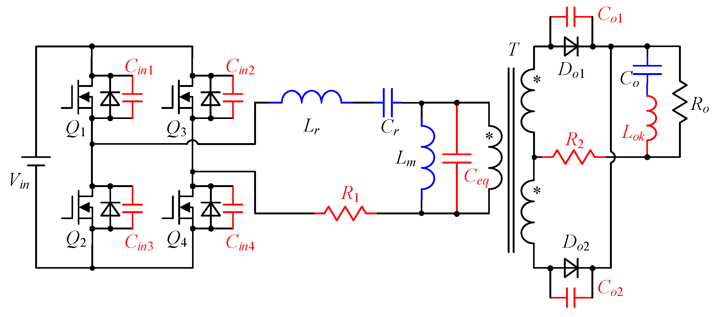
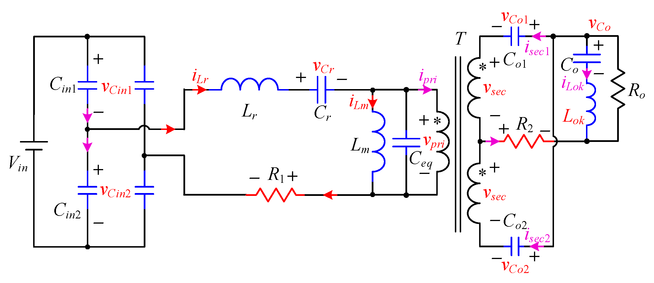
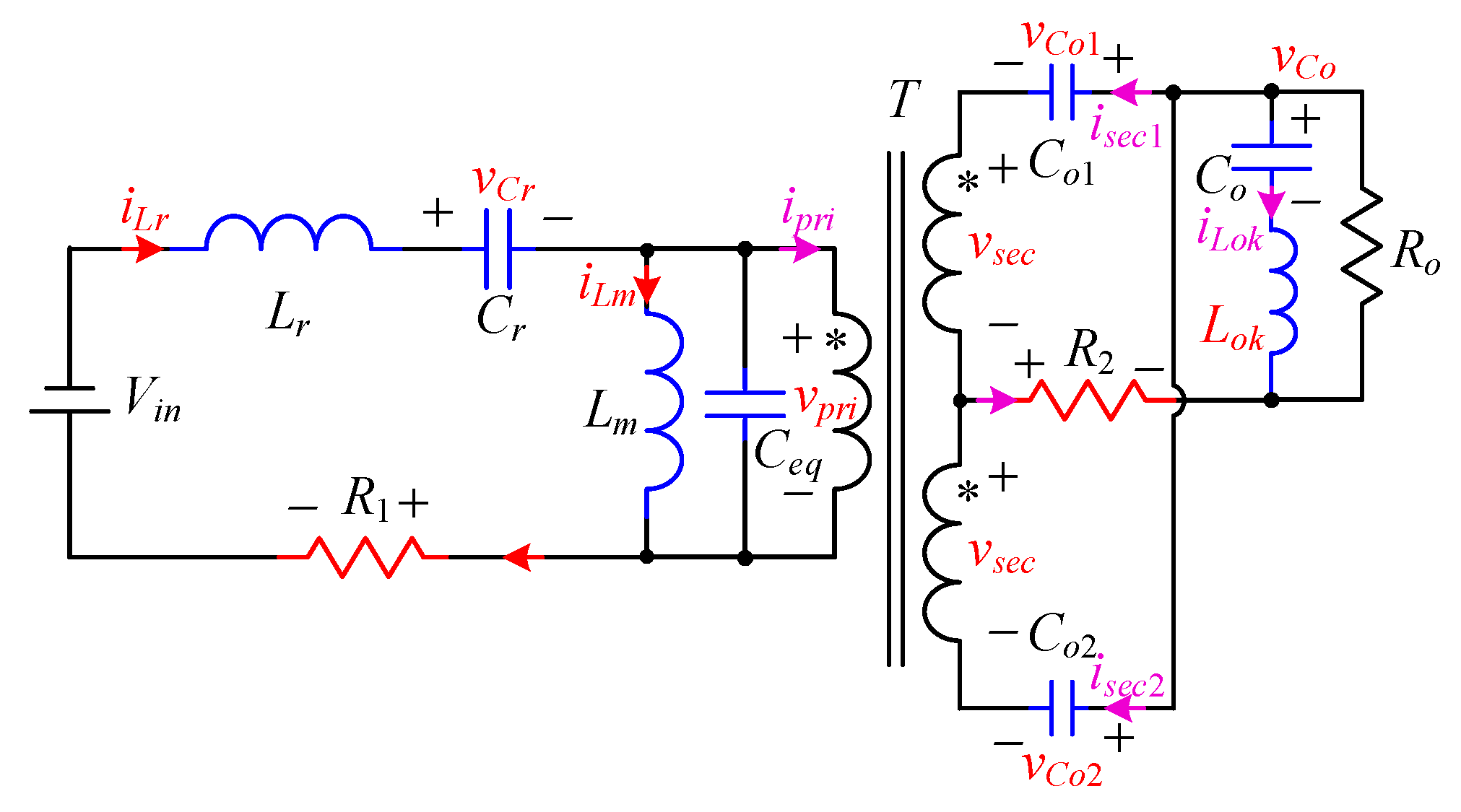
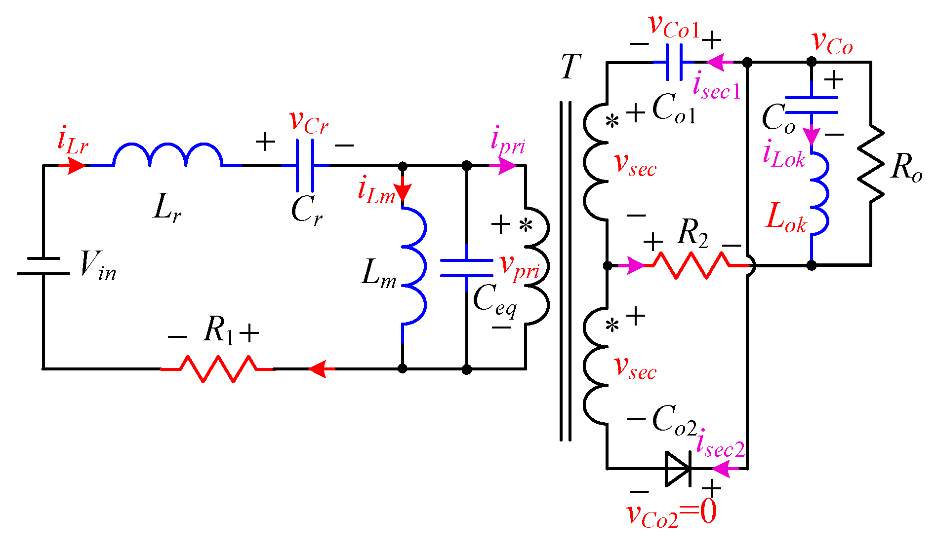
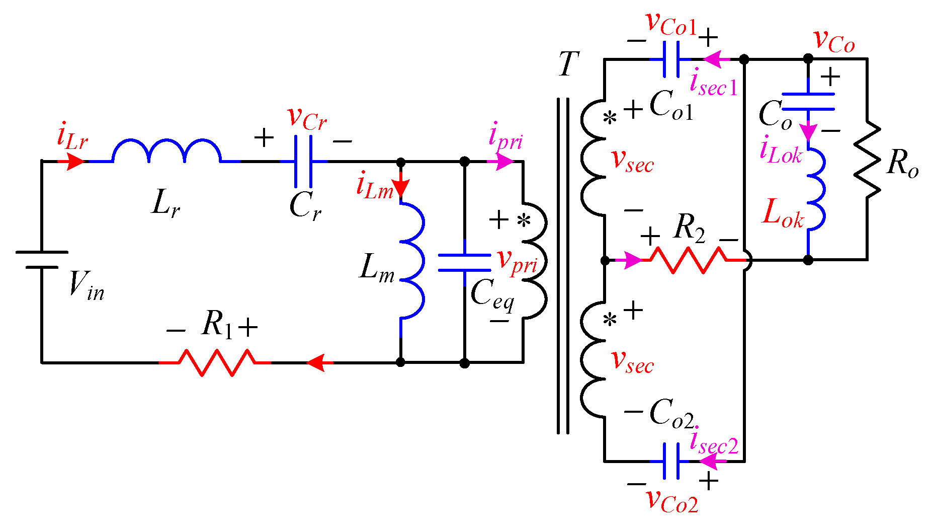
2. Equivalent Circuit of LLC Resonant Converter with Parasitic Components

Figure 1 shows the circuit diagram of a full-bridge LLC resonant converter which considers the parasitic components. The circuit contains the resonant inductance Lr, resonant capacitance Cr, and magnetizing inductance Lm of the transformer T, and also includes the output capacitance Co. In addition to these four necessary ideal passive devices, the parasitic components needing to be considered are:
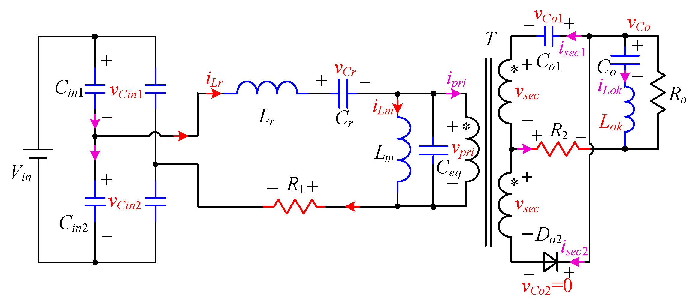
  • the output capacitances of the primary-side SiC MOSFET devices, named as Cin1~Cin4;
  • the equivalent capacitance Ceq of the transformer;
  • the junction capacitances of the rectifier diodes, named as Co1~Co2;
  • the equivalent series inductance Lok of the output capacitance branch;
  • the on-resistance of the switch and the parasitic resistance in the print circuit board (PCB) line of the primary circuit loop are combined and equaled to R1; the influence of the diode voltage drop and the parasitic resistance of the secondary circuit are similarly combined and equaled to R2.

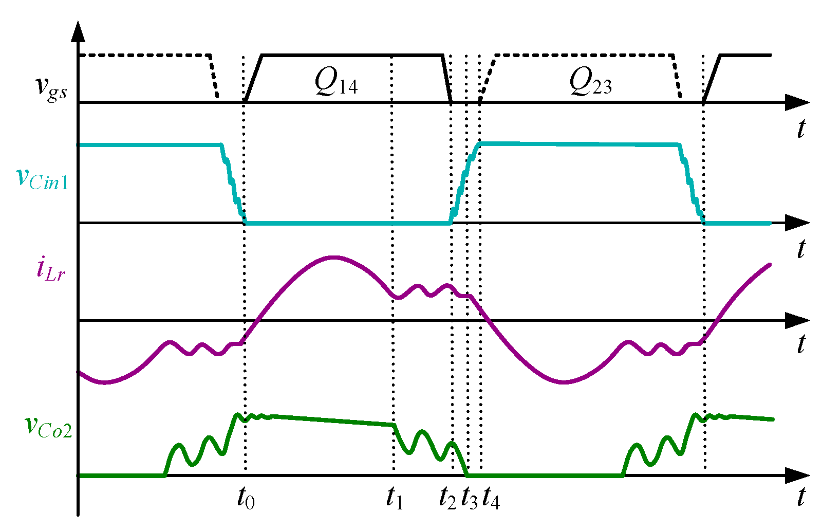
3. Analysis of Operational Principle with Parasitic Components

The most common control strategy for LLC resonant converters is variable frequency control with half duty ratio. To make sure the converter is operating in the ZVS region, the switching frequency is usually lower than the resonant frequency. The circuit waveforms are shown in Figure 2, including the driving waveform vgs, the voltage vCin1 across the switch Q1, the resonant current iLr, and the voltage vCo2 across the rectifier diode Do2.
There are several stages in the waveforms:
• [t0, t1], positive resonant stage. Lr resonates with Cr, and energy is transferred from the primary side to the secondary side. This stage ends when the resonant current is equal to the magnetizing current.
• [t1, t2], since the switching period is longer than the resonance period, there is a freewheeling stage after the end of the resonance. In this stage, the statuses of switches are not changed, and the voltage applied to the resonant network is still Vin. This stage ends when the switches Q1 and Q4 turn off.
• [t2, t4] is the dead time. The voltage across the capacitances of the primary-side switches and the rectifier diodes are changing. This time interval is divided into two stages, the front voltage-establish stage and the rear voltage-establish stage. There are two different voltage-establish modes at different situations.
After t4, the relative switches turn on, and the converter enters the negative resonant stage.

3.1. Freewheeling Stage

When the resonant current is equal to the magnetizing current, the current of the rectifier diode Do1 crosses to zero, and Do1 turns off naturally. Then the converter operates in the freewheeling stage, in which the input voltage of the resonant network is still Vin for the switches Q1 and Q4 are still on. The equivalent circuit in [t1, t2] is shown in Figure 3.
Assume the voltage on the output capacitance is vo, and VRo is the average voltage value on the load Ro at steady state. Therefore, the initial voltages of vCo1 and vCo2 are 0 and 2 VRo on the freewheeling stage. According to the positive direction shown in Figure 3, the relationships of voltages and currents of the LLC converter are list as Equation (A1) in the Appendix A. In which ipri is the primary current of the transformer, isec1 and isec2 are the currents in the two secondary windings respectively. Equation (A1) is complicated and cannot be written as the matrix form directly. To simplify the analysis, several assumptions are made as follows: the voltage VRo is constant, and the voltage change rate of the secondary-side of the transformer is equal to the voltage change rates of vCo2:
d v s e c d t = 1 N d v p r i d t = d v C o 1 d t = d v C o 2 d t ,
in which the transformer turns ratio is N:1:1. Therefore, the resonant current can be solved as:
i L r = i L m + C e q d v p r i d t + i p r i = i L m + ( C e q + C o 1 N 2 + C o 2 N 2 ) d v p r i d t .
The change rates of voltages are:
{ d v p r i d t = i L r i L m C A d v C o 1 d t = d v s e c d t = 1 N d v p r i d t = 1 N i L r i L m C A d v C o 2 d t = d v s e c d t = 1 N d v p r i d t = 1 N i L r i L m C A ,
in which C A = ( C e q + C o 1 N 2 + C o 2 N 2 ) .
Then, the current change rate of output capacitance branch meets:
L o k d i L o k d t = R o C o 1 d v C o 1 d t R o C o 2 d v C o 2 d t i L o k v C o .
In the end, the relationships of voltages and currents in the freewheeling stage can be written as the matrix form of differential equations and list in Equation (A2) in the Appendix A.

3.2. Front Voltage-Establish Stage

After the freewheeling stage, the primary switches Q1 and Q4 turn off, the voltages on capacitances of the primary-side switches and the rectifier diodes are both changing. The equivalent circuit of this stage is shown in Figure 4.
In the traditional analysis, Cin1 and Cin2 are the same, and the currents in those capacitances are at the same value with the opposite direction. However, considering the variation of junction capacitances with the drain-source voltage vds, Cin1 and Cin2 are no longer equal for the initial voltage of Q1 is 0 and the initial voltage of Q2 is Vin. And the currents of the capacitances are no longer same, which satisfy:
i C i n 1 i C i n 2 =   i L r .
Under variable frequency control with half duty ratio in the LLC converter, it can be considered that the voltage change of Q4 is consistent with that of Q1 synchronously. And Q3 is the same as Q2. Therefore, the calculation can be simplified and written as:
{ d i L r d t = v C i n 2 v C i n 1 v C r v p r i R 1 i L r L r d v p r i d t = i L r i L m C A .
The matrix form of differential equations of voltages and currents are list in Equation (A3) in the Appendix A.

3.3. Rear Voltage-Establish Stage

The LLC converter enters to rear voltage-establish stage either vCin2 or vCo2 drops to zero in the front voltage-establish stage. However, the equivalent circuit became different in the next. Two situations need to be discussed separately: primary capacitance voltage-establish mode and secondary capacitance voltage-establish mode. No matter which mode the converter is operating in, after the rear voltage-establish stage, the converter reaches the same stage, i.e., the negative resonant stage.

3.3.1. Primary Capacitance Voltage-Establish Mode

At t3, the voltage of Co2 drops to zero and Do2 turns on, and the primary-side voltage of the transformer drops to −NVo synchronously. Then the energy transfers from the primary side to the secondary side. The equivalent circuit of this mode is shown in Figure 5.
Do2 turns on and vCo2 = 0, then the secondary-side voltage of the transformer satisfies:
v s e c = v C o 1 + v R o + R 2 ( i L o k + v R o R o ) = 0 v R o R 2 ( i L o k + v R o R o ) .
Make simplification and get:
{ v s e c = ( ( 1 + R 2 R o ) v R o + R 2 i L o k ) = 1 2 v C o 1 v R o = ( v s e c R 2 i L o k ) R o R o + R 2 = ( v p r i N R 2 i L o k ) R o R o + R 2 .
Because vRo is the sum of the voltages of the output capacitance and parasitic inductance, as:
v R o = v C o + L o k d i L o k d t .
By calculating, the current changing rate of output capacitance branch is:
d i L o k d t = R o N L o k ( R o + R 2 ) v p r i 1 L o k v C o R o R 2 L o k ( R o + R 2 ) i L o k .
The resonant current and the secondary-side currents are:
{ i L r = i L m + C e q d v p r i d t + i p r i = i L m + C e q d v p r i d t i s e c 1 N + i s e c 2 N i s e c 1 = C o 1 d v C o 1 d t i s e c 2 = i s e c 1 i L o k v R o R o ,
and the change rate of resonant current is:
d i L r d t = v C i n 2 v C i n 1 v C r v p r i R 1 i L r L r .
Then,
d v p r i d t = i L r i L m + 1 N i L o k 1 N 2 ( R o + R 2 ) v p r i R 2 N ( R o + R 2 ) i L o k C B ,
in which C B = C e q + 4 C o 1 N 2 . The matrix form of differential equations can be list as Equation (A4) in the Appendix A.

3.3.2. Secondary Capacitance Voltage-Establish Mode

The other possibility is that vCin1 and vCin2 change to Vin and zero earlier, then the current is freewheeling through the body diodes of primary switches, and the voltage of the input-side of the resonant network is clamped to –Vin. At this mode, since the secondary-side voltage of the transformer is lower than the output voltage, the diode Do2 is still reverse blocking. The equivalent circuit of secondary capacitance voltage-establish mode is shown in Figure 6.
Comparing the equivalent circuit of this mode to that of the free-wheeling stage, it can be found that only the voltage of the input-side of the resonant network changes from Vin to –Vin. Therefore, modify the corresponding coefficient of Equation (A2) can get the differential equations of secondary capacitance voltage-establish mode as Equation (A5) in the Appendix A.

3.4. Negative Resonant Stage

After the rear voltage-establish stage, the voltage of the input-side of the resonant network is clamped to –Vin. The rectifier diode Do2 is conducting forward, and the energy is transferred from the input to the output of the converter. The equivalent circuit is shown in Figure 7.
The differences from Figure 7 to Figure 5 are the voltage of the input side of the resonant network becomes –Vin, and the change rates of vCin1 and vCin2 are both zero. The differences from Figure 7 to Figure 6 are vCo2 is clamped to zero, and Do2 is conducting forward. Then, the matrix form of differential equations of the negative resonant stage can be easily listed as Equation (A6) in the Appendix A.
In the negative resonant stage, the simplified analysis is adopted. No matter whether the primary-side switches Q2 and Q3 are on or not, the equivalent circuit is regarded as the same. The body diodes of primary-side switches could also conduct the resonant current. In practice, the voltage drop of body diode is much higher than that of the on-resistance of the switches. To improve efficiency, the body diode conducting time should be shortened.
In the ideal case, Lr and Cr are resonating during the resonant stage, and primary-side voltage of the transformer is reflected as –NVo. With parasitic components, the negative resonant stage of the LLC converter becomes different. The damping oscillation between parasitic components and the voltage spikes and fluctuations may emerge. Those are both reflected on the voltages of the rectifier diode and the transformer. As a consequence, the voltage stress of the rectifier diodes will increase, and the output voltage will be distorted.

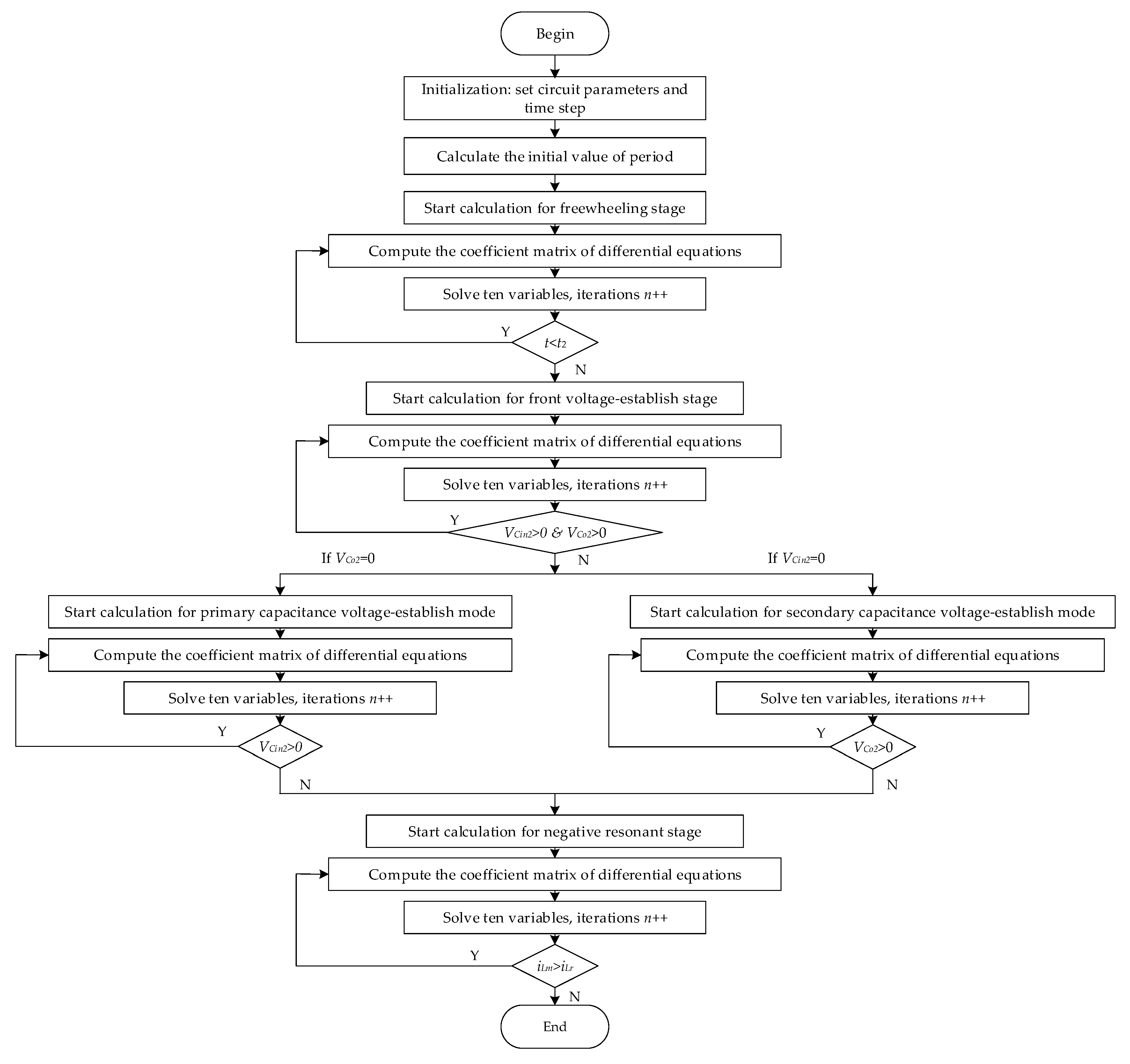
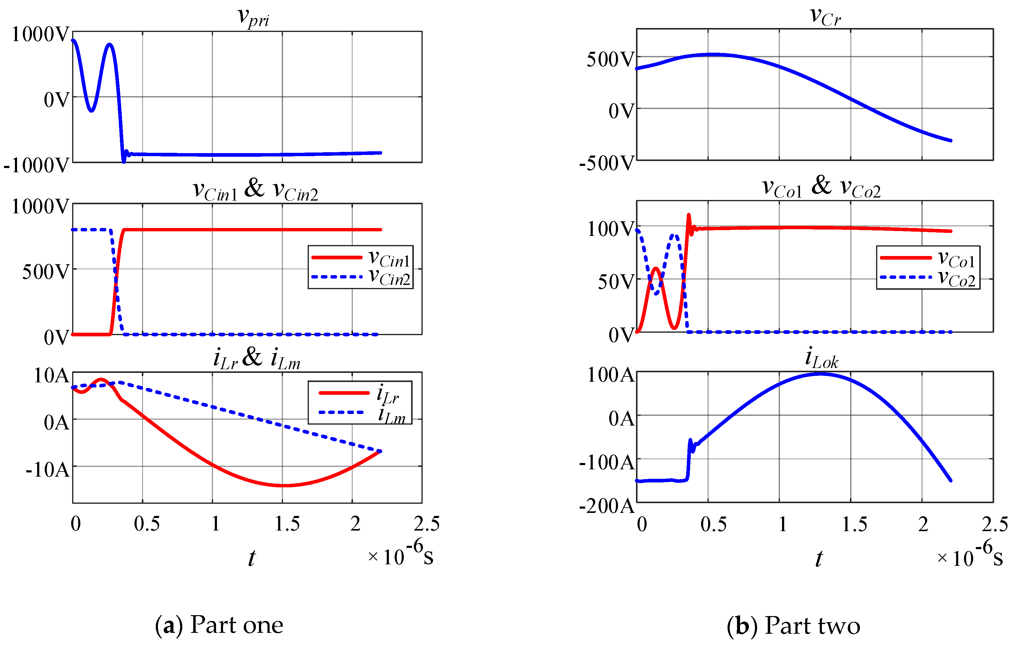
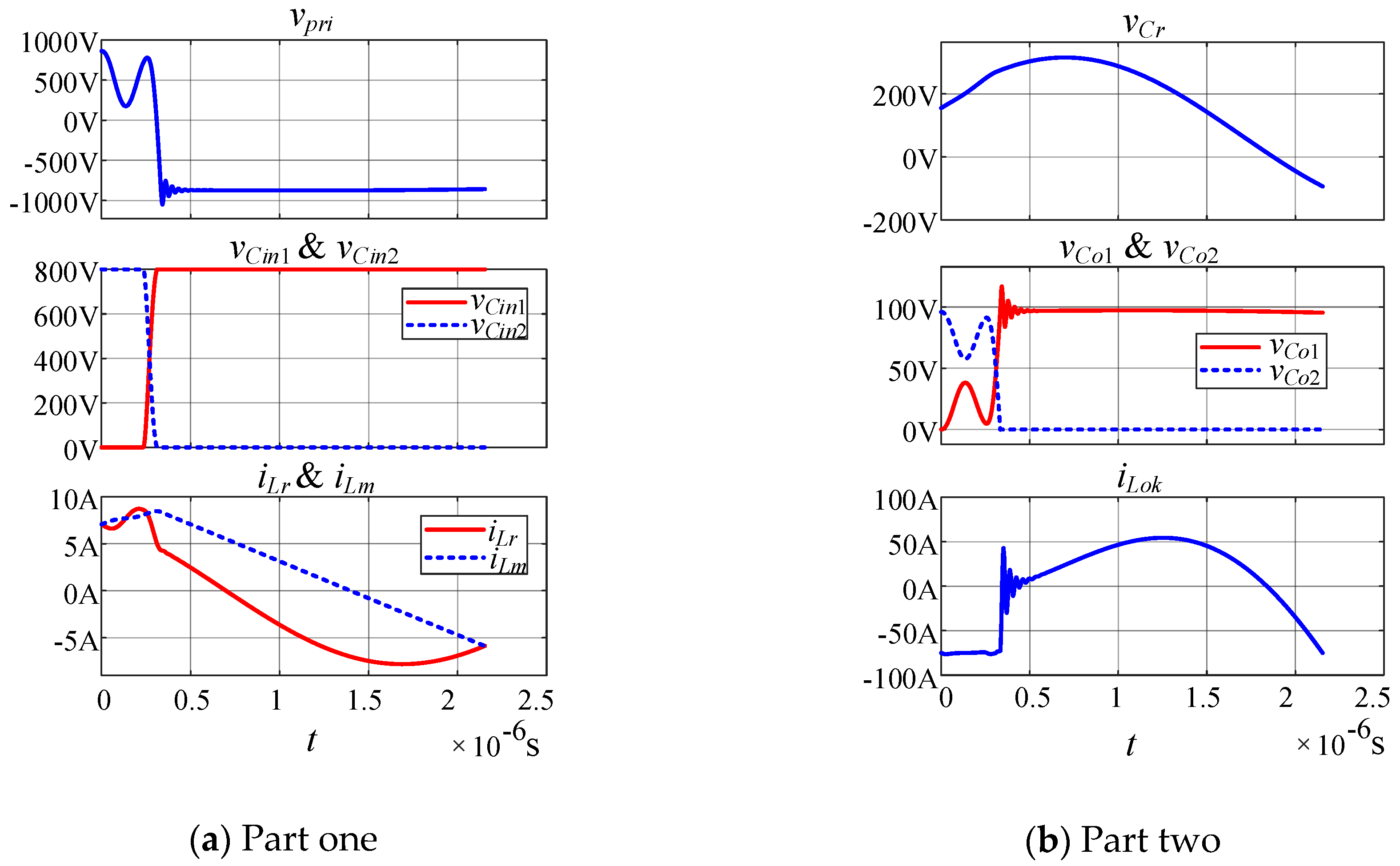
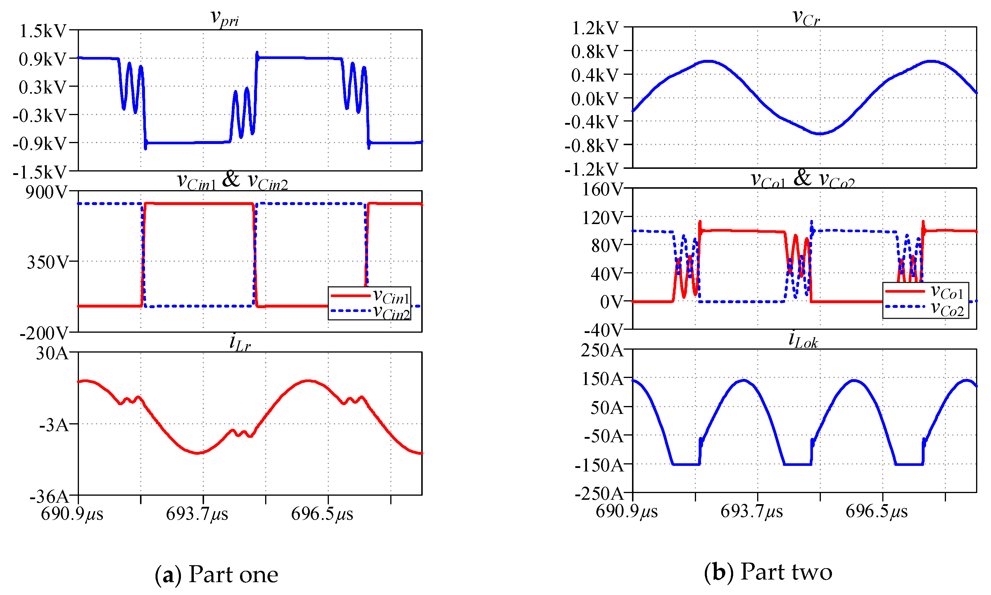
4. Numerical Solution and Simulation Results

4.1. Numerical Solution

Calculate the numerical solution of the differential equations in MATLAB, and Figure 8 shows the flow chart processes of the four stages after the positive resonant stage. The converter parameters and the voltage and current values at time t1 are set at the initialization. Choose two different operating points of the LLC resonant converter to calculate, which correspond to the two kinds of modes. Then, draw the waveforms with changing time as shown in Figure 9 and Figure 10.
In Figure 9, vCo2 drops to zero first, while in Figure 10, vCin2 drops to zero earlier. Besides the resonance between Lr and Cr, there are two other oscillations in the waveforms of the numerical solution.
One oscillation is emerging in the freewheeling stage. The participant components are Lr, Lm, and the capacitance CA. CA includes the Ceq and the reflected capacitances of Co1 and Co2. It is hard to calculate the resonant frequency between these participant components. Since the value of CA is much smaller than the capacitance of Cr, the oscillation frequency is higher than the resonant frequency fr of the LLC converter.
The other oscillation is emerging after vCo2 drops to zero. In Figure 9, the oscillation is in the primary capacitance voltage-establish mode. And in Figure 10, the oscillation is in the negative resonant stage. From the waveform of iLok, it can be seen that there is a significant current step at this time, which leads to a voltage spike. Then, the participant components start to oscillate. Since the parasitic inductance of output capacitance branch is little and the equivalent capacitance CB is small, the oscillation frequency is high. Under the damping effect of R1 and R2, the oscillation decays slowly, overlaying on the main resonance waveform. In Figure 10, due to the secondary capacitance voltage-establish mode, the difference value between the resonant current and the magnetizing current is more significant. As a consequence, a higher spike emerges on the diode voltage and output voltage.
It should be noted that there is an inevitable error, because the error of initial values exists and the influence of the dead time is not considered. Anyway, the deviation is small, and the calculation results of the numerical solution can reflect the operation of the LLC converter considering parasitic components.

4.2. Simulation Results

LTspice software is used to verify the theoretical analysis for it has the advantages such as being free, fast, and easy to converge. And the mathematical model of SiC devices can be imported to LTspice directly. The junction capacitance of the rectifier diode can be represented as a variable current source controlled by variable voltage. To simplify the simulation, the open-loop waveform is simulated with unique driving signals. The LTspice simulation waveforms corresponding to the two kinds of modes are shown in Figure 11 and Figure 12, respectively.
In the LTspice simulation model, all of the parasitic components in the full-bridge LLC resonant converter circuit are considered. The magnetizing current cannot be extracted due to the coupling inductance model of the transformer in LTspice. Compared with the waveforms of the numerical solution of MATLAB, the results are mainly the same with two other oscillations and spikes. However, the length of the freewheeling stage set in the LTspice simulation is slightly larger than that of MATLAB, so the number of oscillation cycles is increased.

5. Design Considerations and Experimental Verification

5.1. Design Considerations of the LLC Converter

Based on the differential equation model and the numerical results, some design considerations of the LLC converter can be given.
  • The dead time for achieving the soft-switching of primary-side switches is related to their output capacitances. However, the output capacitance of switches changes with the drain-source voltage. In the datasheet, the output capacitance is usually given as a curve and the specific value of output capacitance under the specific test condition. In order to simplify the calculation, 2 or 3 times of the specific value of the output capacitance can be used as the equivalent output capacitance in general.
  • The maximum load power should be used in designing the converter parameters. When the load power is maximum, vcr is high and iLr is low in the freewheeling stage. Thus, it is the most serious condition to realize soft-switching of the primary-side switches.
  • The equivalent capacitance of the transformer and the junction capacitance of the rectifier diodes deteriorate the soft-switching of the primary-side switches, and they are both participating in the two oscillations. When designing transformers, the equivalent capacitance should be reduced seriously.
  • The equivalent series inductance Lok of the output capacitance contributes to the voltage spike in the high frequency oscillation, especially for the situation with high output current. Therefore, the output capacitance with small equivalent series inductance should be selected, and the parasitic inductance of the circuit loop should be minimized.

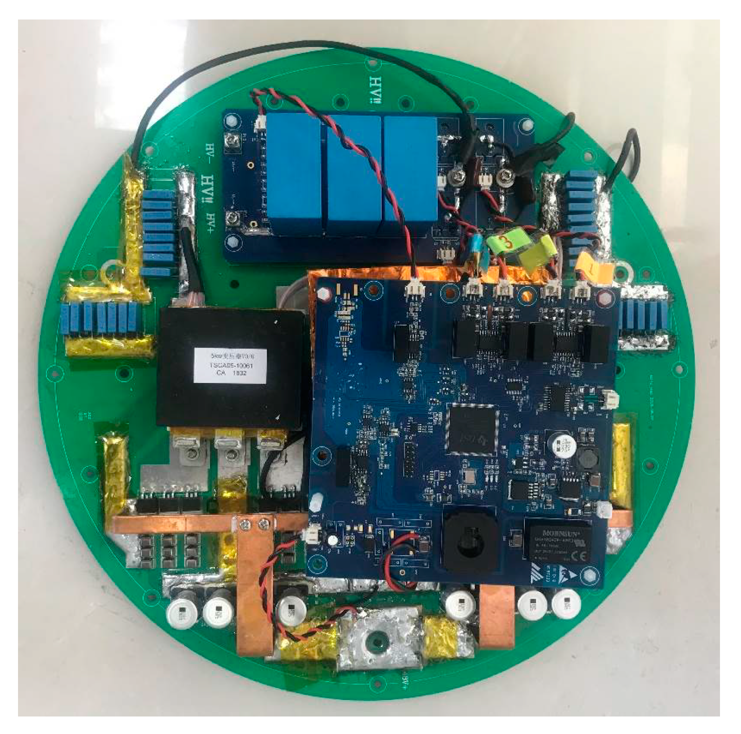
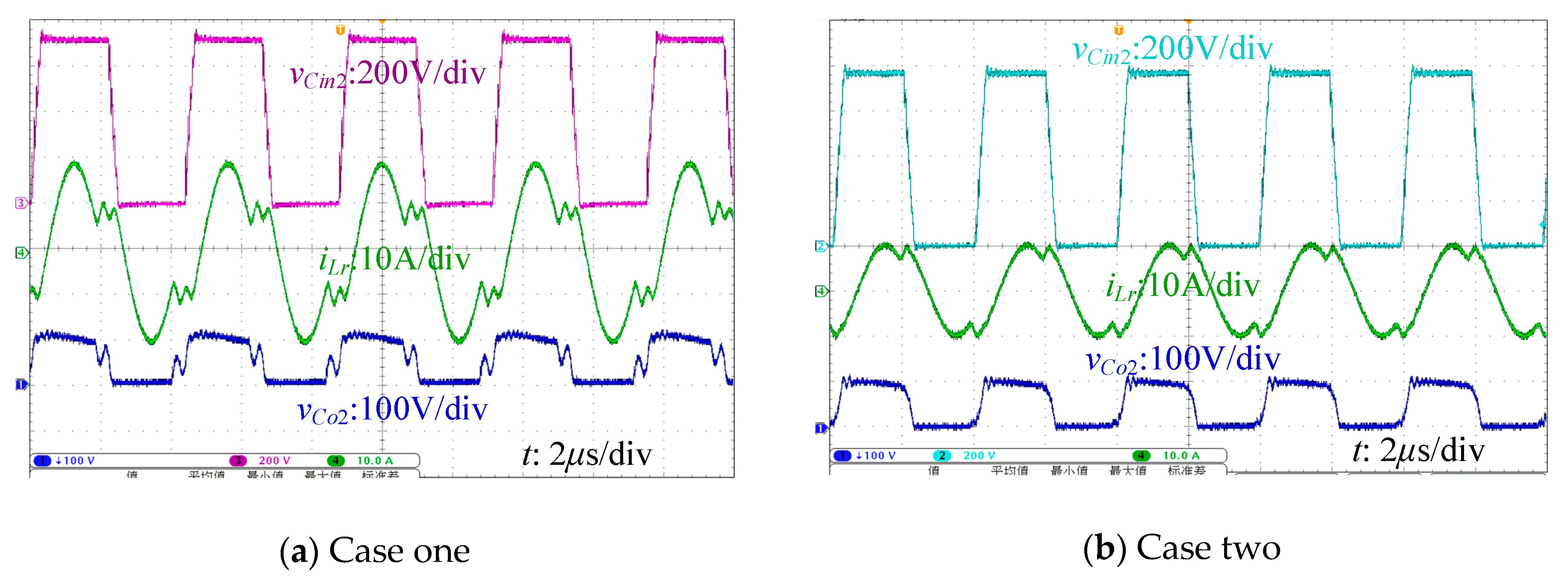
5.2. Experimental Results

In order to verify the assistance of this paper on the design and application of the LLC converter, the specific and concise design procedure based on an application example is given. The design requirements are shown in Table 1.
According to the relationship of the input and output voltages, the transformer turns ratio is defined as 18:1:1. The LLC converter works below the resonant frequency. Set the resonant frequency fr as 255 kHz, and the dead time between switches tdead is 300 ns. The primary-side switches are SiC MOSFETs C2M0025120D. In the datasheet, the output capacitance Coss is 220 pF under the test condition as vgs = 0 V, vds = 1100 V, f = 1 MHz, and vAC = 25 mV.
The traditional LLC resonant converter parameter design process has been given in the references [22,23]. Ignoring the voltage drop of the rectifier diodes, the amplitude of magnetizing current at resonant frequency can be calculated as:
I L m = 1 2 N V R o L m 1 2 f r .
The required dead time to charge and discharge the Coss is:
t d e a d = 2 C o s s V i n I L m .
Therefore, the upper limit value of Lm satisfies:
1 2 N V R o L m 1 2 f r = 2 C o s s V i n t d e a d .
By calculating the parameters of the LLC converter, Lm should be less than 668 μH. However, the soft-switching of primary-side switches cannot be achieved due to the loose restrictions. According to the design considerations proposed in this paper, the actual value of Lm is taken as one sixth to one quarter of the upper limit value calculated by Equation (16), considering the influence of the output capacitance of switches, transformer equivalent parasitic capacitance, and diode junction capacitance. Based on the switching frequency range 160–250 kHz and the voltage gain curves under different switching frequencies, Lm is determined as 6–7 times of Lr in the prototype. Therefore, the final value of Lr is 19.18 μH, and Lm is 111.4 μH. According to the resonant frequency, the value of Cr is 20.25 nF.
In the final design of the prototype, there are two transformers whose primary windings are in series and secondary windings are in parallel after rectifier diodes. The two transformers are the same, in which the turns ratio is 18:2:2 and magnetizing inductances is 55.7 μH. In the design process, the equivalent parasitic capacitance of the transformer should be minimized. When the PCB is drawn, the length of the secondary circuit should be minimized to reduce parasitic inductance. And the symmetry of each secondary circuit should be guaranteed. Those specific optimization methods will not be detailed here. Figure 13 shows the experimental prototype of the LLC converter.
The experimental results of the LLC converter are shown in Figure 14. In case one, the time interval of the freewheeling stage is longer. And iLr and vCo2 are oscillating at a frequency higher than the resonant frequency of the LLC converter. vCo2 drops to zero first, and then vCin2 drops to zero. When the rectifier diode is conducting forward, there is high-frequency oscillation in the beginning of the resonant stage. It is corresponding to the numerical solution and the simulation results. In case two, the time interval of the freewheeling stage is shorter and less than a resonant period. vCin2 drops to zero a little earlier than vCo2. The spike of high-frequency oscillation in the waveforms of diode voltage is a little larger than that of case one.
The experiment results verify the correctness of the differential equation model and its numerical solution. What’s more, the soft-switching of primary-side MOSFETs is achieved based on the parameter design considerations proposed in this paper.

6. Conclusions

The operational principle of the LLC resonant converter with parasitic components is proposed in this paper. Besides the three resonant components, the output capacitance and its parasitic inductance, the capacitance of primary-side switches, the capacitance of rectifier diodes, and the equivalent capacitance of the transformer are all considered. By establishing differential equations and solving numerical solutions, the causes of two different frequency oscillations and the voltage spike are clarified. The simulation results verify the correctness of the theoretical analysis. The influence of the parasitic components and the design considerations are proposed. The experimental results of a specific example of the LLC converter are given. The analysis is helpful in the design and application of the LLC converter.

Author Contributions

F.L., conceptualization, methodology, writing-review and editing; R.H. and X.Y., resources and supervision; H.L., formal analysis, investigation, and validation; X.Z., software and writing-original draft.

Funding

This research was funded by China Postdoctoral Science Foundation (Grant NO. 2019M650466), the Fundamental Research Funds for the Central Universities (Grant No. 2017JBZ101) and the Fundamental Research Funds for the Central Universities (Grant No. 2017YJS176).

Conflicts of Interest

The authors declare no conflict of interest.

Appendix A

The voltage and current expressions of freewheeling stage:
{ V i n = L r d i L r d t + v C r + v p r i + R 1 i L r i L r = i L m + C e q d v p r i d t + i p r i v p r i = L m d i L m d t i L r = C r d v C r d t v C i n 1 = 0 , v C i n 2 = V i n v s e c = v C o 1 + v R o + R 2 ( i L o k + v R o R o ) , v p r i = N v s e c v s e c = v C o 2 v R o R 2 ( i L o k + v R o R o ) i s e c 1 = C o 1 d v C o 1 d t , i s e c 2 = C o 2 d v C o 2 d t i p r i = i s e c 1 N + i s e c 2 N C o d v C o d t = i L o k v R o = v C o + L o k d i L o k d t = R o ( C o 1 d v C o 1 d t C o 2 d v C o 2 d t i L o k ) .
The differential equation model of freewheeling stage:
( i ˙ L r v ˙ C r i ˙ L m v ˙ p r i v ˙ C i n 1 v ˙ C i n 2 v ˙ C o 1 v ˙ C o 2 i ˙ L o k v ˙ C o ) = ( R 1 L r 1 L r 0 1 L r 0 0 0 0 0 0 1 C r 0 0 0 0 0 0 0 0 0 0 0 0 1 L m 0 0 0 0 0 0 1 C A 0 1 C A 0 0 0 0 0 0 0 0 0 0 0 0 0 0 0 0 0 0 0 0 0 0 0 0 0 0 0 1 N C A 0 1 N C A 0 0 0 0 0 0 0 1 N C A 0 1 N C A 0 0 0 0 0 0 0 R o ( C o 1 C o 2 ) N C A L o k 0 R o ( C o 1 C o 2 ) N C A L o k 0 0 0 0 0 R o L o k 1 L o k 0 0 0 0 0 0 0 0 1 C o 0 ) ( i L r v C r i L m v p r i v C i n 1 v C i n 2 v C o 1 v C o 2 i L o k v C o ) + ( V i n L r 0 0 0 0 0 0 0 0 0 ) .
The differential equation model of front voltage-establish stage:
( i ˙ L r v ˙ C r i ˙ L m v ˙ p r i v ˙ C i n 1 v ˙ C i n 2 v ˙ C o 1 v ˙ C o 2 i ˙ L o k v ˙ C o ) = ( R 1 L r 1 L r 0 1 L r 1 L r 1 L r 0 0 0 0 0 1 C r 0 0 0 0 0 0 0 0 0 0 0 0 1 L m 0 0 0 0 0 0 1 C A 0 1 C A 0 0 0 0 0 0 0 1 C i n 1 + C i n 2 0 0 0 0 0 0 0 0 0 1 C i n 1 + C i n 2 0 0 0 0 0 0 0 0 0 1 N C A 0 1 N C A 0 0 0 0 0 0 0 1 N C A 0 1 N C A 0 0 0 0 0 0 0 R o ( C o 1 C o 2 ) N C A L o k 0 R o ( C o 1 C o 2 ) N C A L o k 0 0 0 0 0 R o L o k 1 L o k 0 0 0 0 0 0 0 0 1 C o 0 ) ( i L r v C r i L m v p r i v C i n 1 v C i n 2 v C o 1 v C o 2 i L o k v C o ) + ( 0 0 0 0 0 0 0 0 0 0 ) .
The differential equation model of rear voltage-establish stage with primary capacitance voltage-establish mode:
( i ˙ L r v ˙ C r i ˙ L m v ˙ p r i v ˙ C i n 1 v ˙ C i n 2 v ˙ C o 1 v ˙ C o 2 i ˙ L o k v ˙ C o ) = ( R 1 L r 1 L r 0 1 L r 1 L r 1 L r 0 0 0 0 1 C r 0 0 0 0 0 0 0 0 0 0 0 0 1 L m 0 0 0 0 0 0 1 C B 0 1 C B 1 N 2 C B ( R o + R 2 ) 0 0 0 0 R o N C B ( R o + R 2 ) 0 1 C i n 1 + C i n 2 0 0 0 0 0 0 0 0 0 1 C i n 1 + C i n 2 0 0 0 0 0 0 0 0 0 2 N C B 0 2 N C B 2 N 3 C B ( R o + R 2 ) 0 0 0 0 2 R o N 2 C B ( R o + R 2 ) 0 0 0 0 0 0 0 0 0 0 0 0 0 0 R o N L o k ( R o + R 2 ) 0 0 0 0 R o R 2 L o k ( R o + R 2 ) 1 L o k 0 0 0 0 0 0 0 0 1 C o 0 ) ( i L r v C r i L m v p r i v C i n 1 v C i n 2 v C o 1 v C o 2 i L o k v C o ) + ( 0 0 0 0 0 0 0 0 0 0 ) .
The differential equation model of rear voltage-establish stage with secondary capacitance voltage-establish mode:
( i ˙ L r v ˙ C r i ˙ L m v ˙ p r i v ˙ C i n 1 v ˙ C i n 2 v ˙ C o 1 v ˙ C o 2 i ˙ L o k v ˙ C o ) = ( R 1 L r 1 L r 0 1 L r 0 0 0 0 0 0 1 C r 0 0 0 0 0 0 0 0 0 0 0 0 1 L m 0 0 0 0 0 0 1 C A 0 1 C A 0 0 0 0 0 0 0 0 0 0 0 0 0 0 0 0 0 0 0 0 0 0 0 0 0 0 0 1 N C A 0 1 N C A 0 0 0 0 0 0 0 1 N C A 0 1 N C A 0 0 0 0 0 0 0 R o ( C o 1 C o 2 ) N C A L o k 0 R o ( C o 1 C o 2 ) N C A L o k 0 0 0 0 0 R o L o k 1 L o k 0 0 0 0 0 0 0 0 1 C o 0 ) ( i L r v C r i L m v p r i v C i n 1 v C i n 2 v C o 1 v C o 2 i L o k v C o ) + ( V i n L r 0 0 0 0 0 0 0 0 0 ) .
The differential equation model of negative resonant stage:
( i ˙ L r v ˙ C r i ˙ L m v ˙ p r i v ˙ C i n 1 v ˙ C i n 2 v ˙ C o 1 v ˙ C o 2 i ˙ L o k v ˙ C o ) = ( R 1 L r 1 L r 0 1 L r 0 0 0 0 0 0 1 C r 0 0 0 0 0 0 0 0 0 0 0 0 1 L m 0 0 0 0 0 0 1 C B 0 1 C B 1 N 2 C B ( R o + R 2 ) 0 0 0 0 R o N C B ( R o + R 2 ) 0 0 0 0 0 0 0 0 0 0 0 0 0 0 0 0 0 0 0 0 0 2 N C B 0 2 N C B 2 N 3 C B ( R o + R 2 ) 0 0 0 0 2 R o N 2 C B ( R o + R 2 ) 0 0 0 0 0 0 0 0 0 0 0 0 0 0 R o N L o k ( R o + R 2 ) 0 0 0 0 R o R 2 L o k ( R o + R 2 ) 1 L o k 0 0 0 0 0 0 0 0 1 C o 0 ) ( i L r v C r i L m v p r i v C i n 1 v C i n 2 v C o 1 v C o 2 i L o k v C o ) + ( V i n L r 0 0 0 0 0 0 0 0 0 ) .

References

  1. Bhuvaneswari, C.; Babu, R.S.R. A review on LLC Resonant Converter. In Proceedings of the International Conference on Computation of Power, Energy Information and Communication (ICCPEIC), Chennai, India, 20–21 April 2016; pp. 620–623. [Google Scholar]
  2. Lu, B.; Liu, W.; Liang, Y.; Lee, F.C.; Wyk, J.D. Optimal design methodology for LLC resonant converter. In Proceedings of the Twenty-First Annual IEEE Applied Power Electronics Conference and Exposition, 2006. APEC ’06, Dallas, TX, USA, 3 March 2006; pp. 533–538. [Google Scholar]
  3. Yang, B.; Lee, F.C.; Zhang, A.J.; Huang, G. Resonant converter for front end DC/DC conversion. In Proceedings of the APEC. Seventeenth Annual IEEE Applied Power Electronics Conference and Exposition (Cat. No.02CH37335), Dallas, TX, USA, 10–14 March 2002; Volume 2, pp. 1108–1112. [Google Scholar]
  4. Gu, Y.; Lu, Z.Y.; Hang, L.J.; Qian, Z.M.; Huang, G.S. Three-level LLC series resonant DC/DC converter. IEEE Trans. Power Electron. 2005, 20, 781–789. [Google Scholar] [CrossRef]
  5. Chen, H.; Wu, X. Analysis on the influence of the secondary parasitic capacitance to ZVS transient in LLC resonant converter. In Proceedings of the 2014 IEEE Energy Conversion Congress and Exposition (ECCE), Pittsburgh, PA, USA, 14–18 September 2014; pp. 4755–4760. [Google Scholar]
  6. Wang, N.; Jia, H.; Tian, M.; Li, Z.; Xu, G.; Yang, X. Impact of transformer stray capacitance on the conduction loss in a GaN-based LLC resonant converter. In Proceedings of the 2017 IEEE 3rd International Future Energy Electronics Conference and ECCE Asia (IFEEC 2017 - ECCE Asia), Kaohsiung, Taiwan, 3–7 June 2017; pp. 1334–1338. [Google Scholar]
  7. Wang, N.; Yang, X.; Tian, M.; Jia, H.; Xu, G.; Li, Z. An Optimal Design Method Considering Transformer Parasitic Capacitance of LLC Resonant Converters. In Proceedings of the 2018 International Power Electronics Conference (IPEC-Niigata 2018—ECCE Asia), Niigata, Japan, 20–24 May 2018; pp. 998–1003. [Google Scholar]
  8. Sato, M.; Nagaoka, S.; Uematsu, S.; Zaitsu, T. Mechanism of Current Imbalance in LLC resonant converter with Center Tapped Transformer. In Proceedings of the 2018 International Power Electronics Conference (IPEC-Niigata 2018 -ECCE Asia), Niigata, Japan, 20–24 May 2018; pp. 118–122. [Google Scholar]
  9. Li, M.; Chen, Q.; Ren, X.; Zhang, Y.; Jin, K.; Chen, B. The integrated LLC resonant converter using center-tapped transformer for on-board EV charger. In Proceedings of the 2015 IEEE Energy Conversion Congress and Exposition (ECCE), Montreal, QC, Canada, 20–24 September 2015; pp. 6293–6298. [Google Scholar]
  10. Park, K.B.; Kim, B.C.; Lee, B.H.; Kim, C.E.; Moon, G.W.; Youn, M.J. Analysis and design of LLC resonant converter considering rectifier voltage oscillation. In Proceedings of the 2009 IEEE Energy Conversion Congress and Exposition, San Jose, CA, USA, 20–24 September 2009; pp. 771–775. [Google Scholar]
  11. Park, K.; Lee, B.; Moon, G.; Youn, M. Analysis on Center-Tap Rectifier Voltage Oscillation of LLC Resonant Converter. IEEE Trans. Power Electron. 2012, 27, 2684–2689. [Google Scholar] [CrossRef]
  12. Lee, B.H.; Kim, M.Y.; Kim, C.E.; Park, K.B.; Moon, G.W. Analysis of LLC Resonant Converter considering effects of parasitic components. In Proceedings of the INTELEC 2009—31st International Telecommunications Energy Conference, Incheon, South Korea, 18–22 October 2009; pp. 1–6. [Google Scholar]
  13. Hariya, A.; Yanagi, H.; Ishizuka, Y.; Matsuura, K.; Tomioka, A.; Ninomiya, T. Influence of parasitic components on MHz-level frequency LLC resonant DC-DC converter. In Proceedings of the IECON 2015—41st Annual Conference of the IEEE Industrial Electronics Society, Yokohama, Japan, 9–12 November 2015; pp. 4842–4847. [Google Scholar]
  14. Kim, J.H.; Kim, C.E.; Kim, J.K.; Moon, G.W. Analysis for LLC resonant converter considering parasitic components at very light load condition. In Proceedings of the 8th International Conference on Power Electronics - ECCE Asia, Jeju, South Korea, 30 May–3 June 2011; pp. 1863–1868. [Google Scholar]
  15. Feng, W. State-Trajectory Analysis and Control of LLC Resonant Converters. Doctor Dissertations, Virginia Polytechnic Institute and State University, Blacksburg, Virginia, 29 March 2013. [Google Scholar]
  16. Liu, J.; Zhang, J.; Zheng, T.Q.; Yang, J. A Modified Gain Model and the Corresponding Design Method for an LLC Resonant Converter. IEEE Trans. Power Electron. 2017, 32, 6716–6727. [Google Scholar] [CrossRef]
  17. Ivensky, G.; Bronshtein, S.; Abramovitz, A. Approximate Analysis of Resonant LLC DC-DC Converter. IEEE Trans. Power Electron. 2011, 26, 3274–3284. [Google Scholar] [CrossRef]
  18. Kwon, M.; Lee, W. A Study on the Analysis and Control of No-load Characteristics of LLC Resonant Converter for Plasma Process. In Proceedings of the 2018 International Power Electronics Conference (IPEC-Niigata 2018 -ECCE Asia), Niigata, Japan, 20–24 May 2018; pp. 114–117. [Google Scholar]
  19. Kim, J.H.; Kim, C.E.; Kim, J.K.; Lee, J.B.; Moon, G.W. Analysis on Load Adaptive Phase-Shift Control for High Efficiency Full-Bridge LLC Resonant Converter in Light Load Conditions. IEEE Trans. Power Electron. 2016, 31, 4942–4955. [Google Scholar] [CrossRef]
  20. Ahmed, M.R.; Todd, R.; Forsyth, A.J. Analysis of SiC MOSFETs under hard and soft-switching. In Proceedings of the 2015 IEEE Energy Conversion Congress and Exposition (ECCE), Montreal, QC, Canada, 20–24 September 2015; pp. 2231–2238. [Google Scholar]
  21. Ahmed, M.R.; Todd, R.; Forsyth, A.J. Predicting SiC MOSFET Behavior Under Hard-Switching, Soft- Switching, and False Turn-On Conditions. IEEE Trans. Ind. Electron. 2017, 64, 9001–9011. [Google Scholar] [CrossRef]
  22. Infineon Technologies. Design Guide for LLC Converter with ICE2HS01G. Application Note, V1.0. Available online: https://www.infineon.com/dgdl/Infineon-Design guide LLC_ converter ICE2HS01G-AN-v0100-EN. pdf?fileId= db3a304330f68606013103ebd94f3e98 (accessed on 1 July 2011).
  23. Wu, X.; Chen, H.; Qian, Z. 1-MHz LLC Resonant DC Transformer (DCX) With Regulating Capability. IEEE Trans. Ind. Electron. 2016, 63, 2904–2912. [Google Scholar] [CrossRef]
Figure 1. Full-bridge LLC resonant converter circuit with parasitic components.
Energies 12 04305 g001
Figure 2. Key waveforms of full-bridge LLC resonant converter considering parasitic components.
Energies 12 04305 g002
Figure 3. The equivalent circuit of the freewheeling stage.
Energies 12 04305 g003
Figure 4. The equivalent circuit of the front voltage-establish stage.
Energies 12 04305 g004
Figure 5. The equivalent circuit of the primary capacitance voltage-establish mode.
Energies 12 04305 g005
Figure 6. The equivalent circuit of the secondary capacitance voltage-establish mode.
Energies 12 04305 g006
Figure 7. The equivalent circuit of the negative resonant stage.
Energies 12 04305 g007
Figure 8. The flow chart of the solution processes in MATLAB.
Energies 12 04305 g008
Figure 9. The waveforms of the numerical solution with primary capacitance voltage-establish mode.
Energies 12 04305 g009
Figure 10. The waveforms of the numerical solution with secondary capacitance voltage-establish mode.
Energies 12 04305 g010
Figure 11. The LTspice simulation results of the LLC converter with primary capacitance voltage-establish mode.
Energies 12 04305 g011
Figure 12. The LTspice simulation results of the LLC converter with secondary capacitance voltage-establish mode.
Energies 12 04305 g012
Figure 13. The experimental prototype of the LLC converter.
Energies 12 04305 g013
Figure 14. The experimental results of the LLC converter.
Energies 12 04305 g014
Table 1. The parameters of the LLC experimental prototype.
ParametersValue
Input voltage700–800 V
Output voltage48 V
Rated power8000 W
Primary switchesC2M0025120D
Rectifier diodesVB60170G

