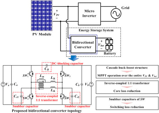
1. Introduction
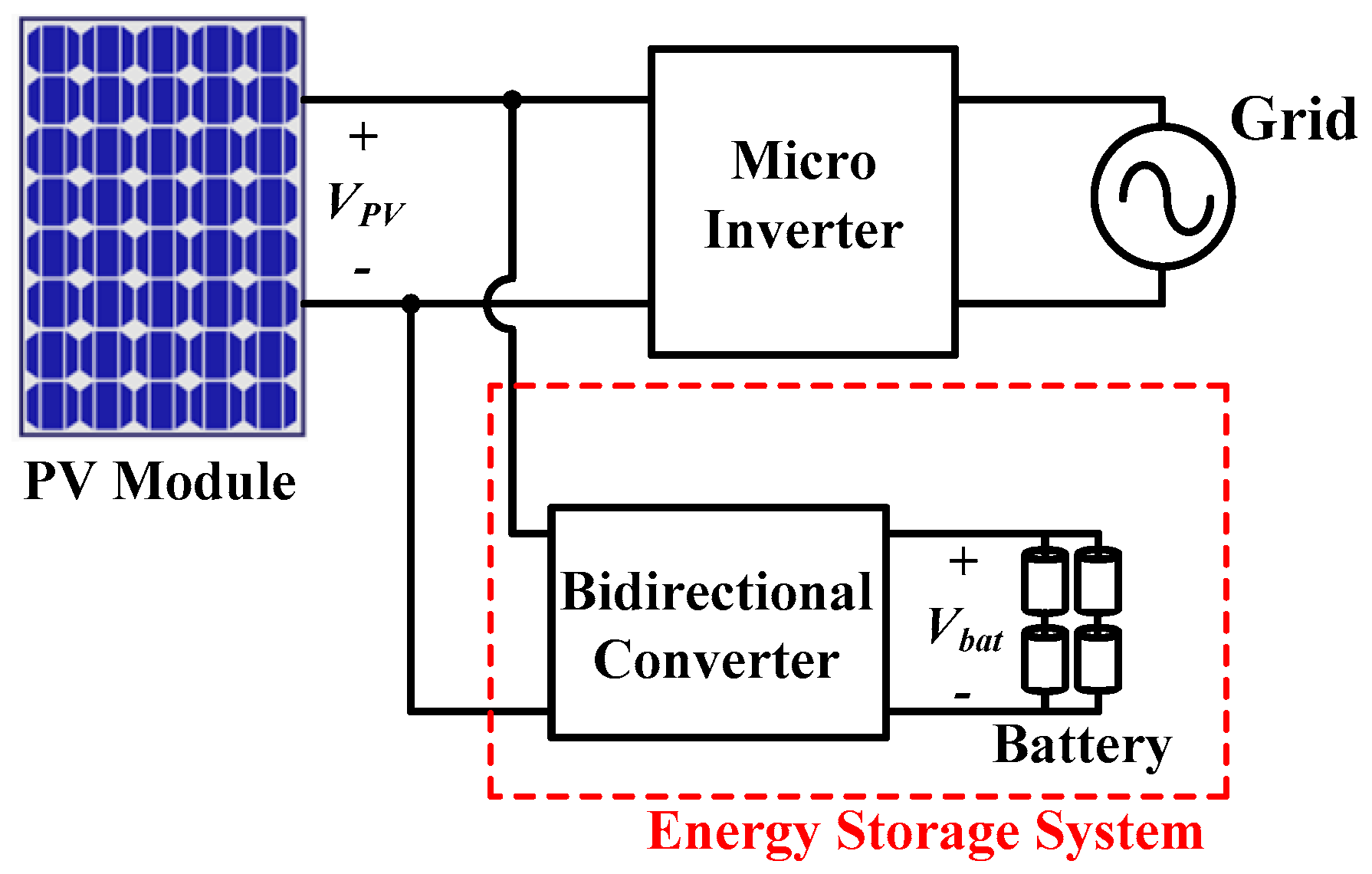
Distributed generation (DG) is the future of energy systems that provide system reliability and flexibility within local electric loads instead of centralized generation. DG mainly uses renewable energy sources, which provide irregular power depending on weather conditions. Therefore, to stabilize the power, DG (
Figure 1) requires an energy storage system (ESS) consisting of a battery and a bidirectional converter (BDC) [
1,
2,
3,
4,
5]. BDC is essential for the ESS because it needs to be able to charge the battery with the power supplied from DG and to transfer energy from the battery to the grid when the DG runs out of power.
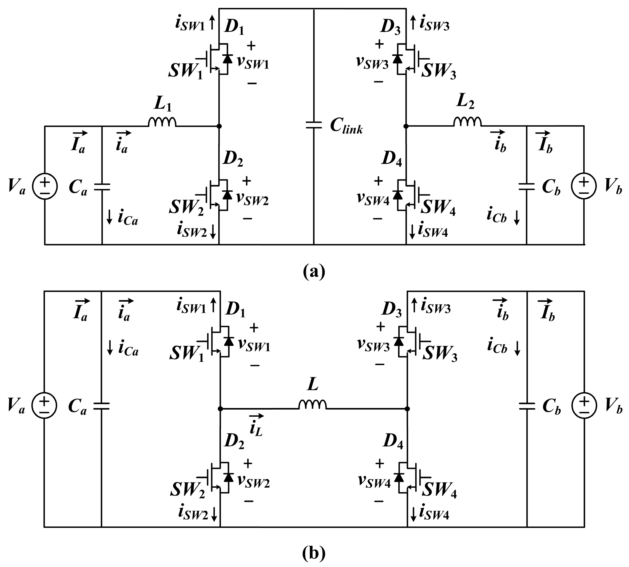
The basic BDCs mainly use the combined half-bridge (CHB) and the cascade buck–boost (CBB) structures (
Figure 2). The CHB converter (
Figure 2a) has two power stages consisting of two half-bridge converters and a dc link capacitor
Clink that operates as an energy-transfer unit [
6,
7,
8]. One power stage performs the buck operation and the other stage performs the boost operation. An additional half-bridge converter can be connected to the
Clink in order to use the converter as multiple inputs or outputs. The CBB converter [
9,
10,
11,
12,
13,
14] (
Figure 2b) consists of one inductor and four switches.
In a similar way to CHB, the switches on the left leg are used for the buck operation and the switches on the right leg are used for the boost operation. The CBB converter can be implemented in a smaller size to the CHB converter because it uses only one inductor. These converters have simple structure and control method, but they have some drawbacks because the converter must be operated in discontinuous conduction mode (DCM) at full load for zero voltage turn-on. Further, (1) if the converter is operated at a fixed frequency, the inductor reverse current increases under light load conditions, increasing conduction losses; (2) the current ripple in the inductor causes core loss and increases output voltage ripple; and (3) the high-frequency operation of the converter is undesirable because the turn-off switching loss is significantly increased when the converter is not operating in DCM.
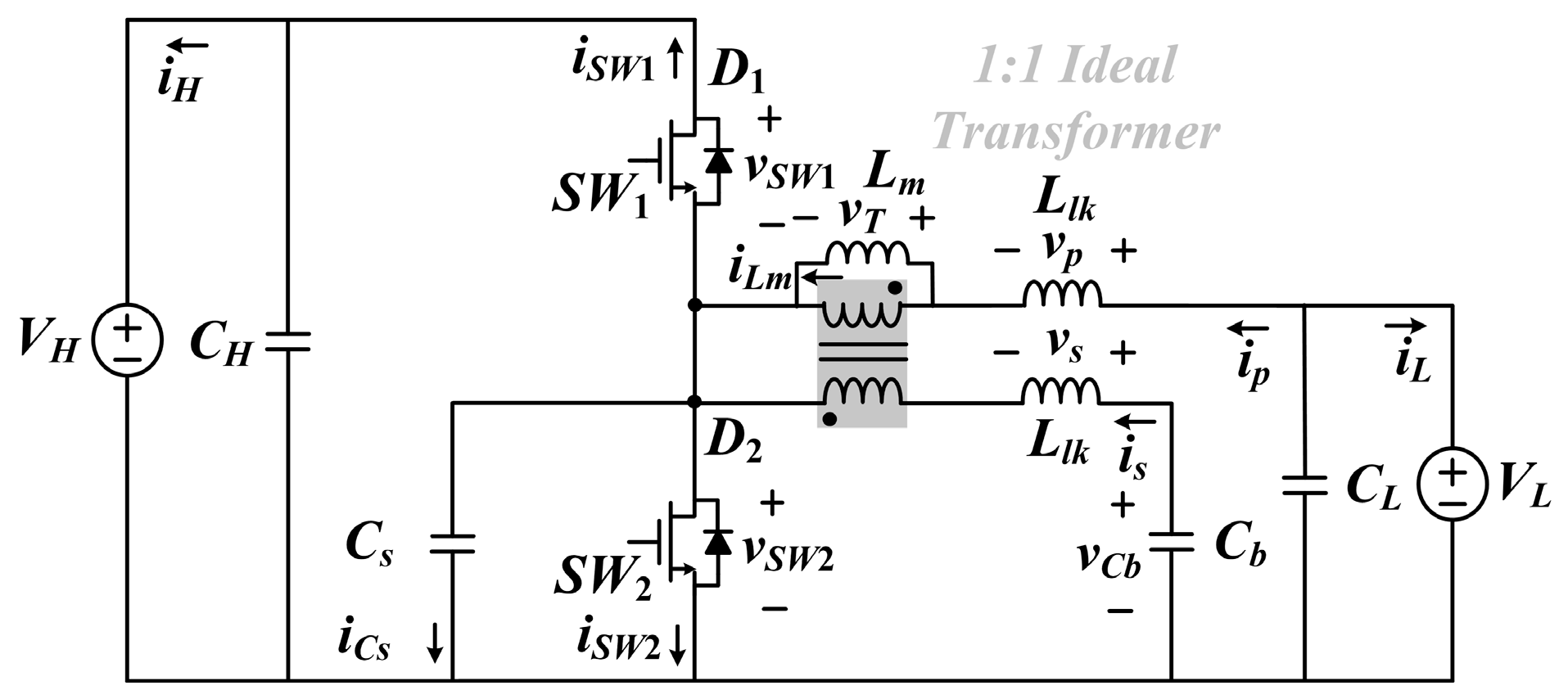
The converter of [
15] used an inverse coupled 1:1 transformer and pulse-frequency modulation to solve the above problems. The converter consists of a 1:1 transformer, a dc-blocking capacitor
Cb, a snubber capacitor
Cs, and two switches
SW1 and
SW2 (
Figure 3). The windings of the transformer are connected in a series-aiding configuration to minimize ripple of the magnetizing current
iLm, which causes major core losses.
Cs reduces the switching loss by lowering the turn-on and turn-off slopes of the switch voltages. The converter of [
15] can improve the efficiency and operate at high switching frequency because the 1:1 transformer and
Cs reduce the core loss and switching loss.
However, despite these advantages, the converter of [
15] is difficult to use in ESSs. The circuit of [
15] assumes
VH >
VL—that is, that the direction of the buck conversion is from left to right and the direction of the boost conversion is from right to left. Therefore, this converter cannot be used when the input voltage range overlaps with the output voltage range. A typical PV–ESS system for home applications has been built using PV panels with an operating voltage range of 25–50 V [
16,
17,
18] and batteries with an operating voltage range of 42–58.8 V [
19,
20,
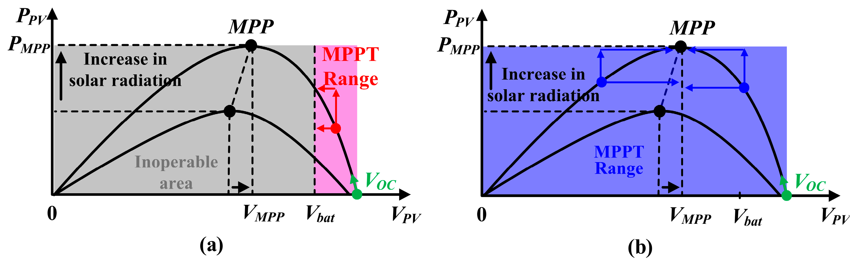
21]. For a given solar irradiation dose, the converter of the PV–ESS system adjusts the switching duty
D to convert the PV voltage
VPV =
VIN to the battery charge voltage
Vbat =
VO. For the buck conversion,
VPV decreases as
D increases because the converter draws more current from the input filter capacitor
CIN. The photovoltaic power
PPV increases as
VPV decreases until
VPV reaches the maximum power point (MPP) voltage
VMPP (
Figure 4); further reduction of
VPV reduces
PPV. MPP moves when the solar irradiation on the PV panel changes. For
VMPP <
Vbat <
VOC, the range of the maximum power point tracking (MPPT) operation for the circuit of [
15] is limited to
Vbat <
VPV <
VOC (
Figure 4a). When 25 V <
VPV < 50 V and 42 V <
Vbat < 58.8 V (i.e., the general operation range of PV–ESS), the circuit of [
15] has to use three series-connected PV panels and one battery for buck mode operation, or one PV panel and two-series connected batteries for boost mode operation. Serially connected batteries have a balancing problem. Separate MPPT control is not possible for serially connected PV panels, which means that optimum MPPT efficiency cannot be achieved.
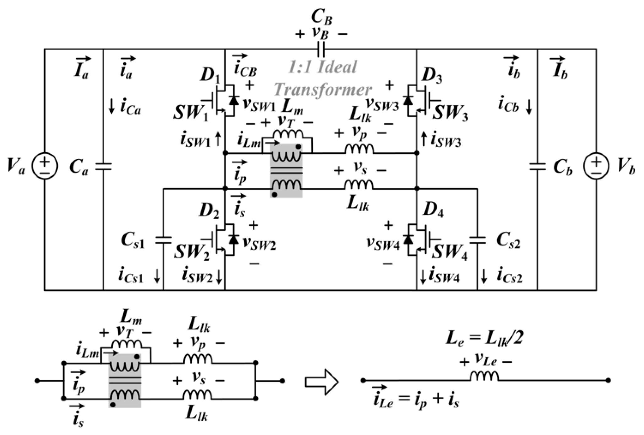
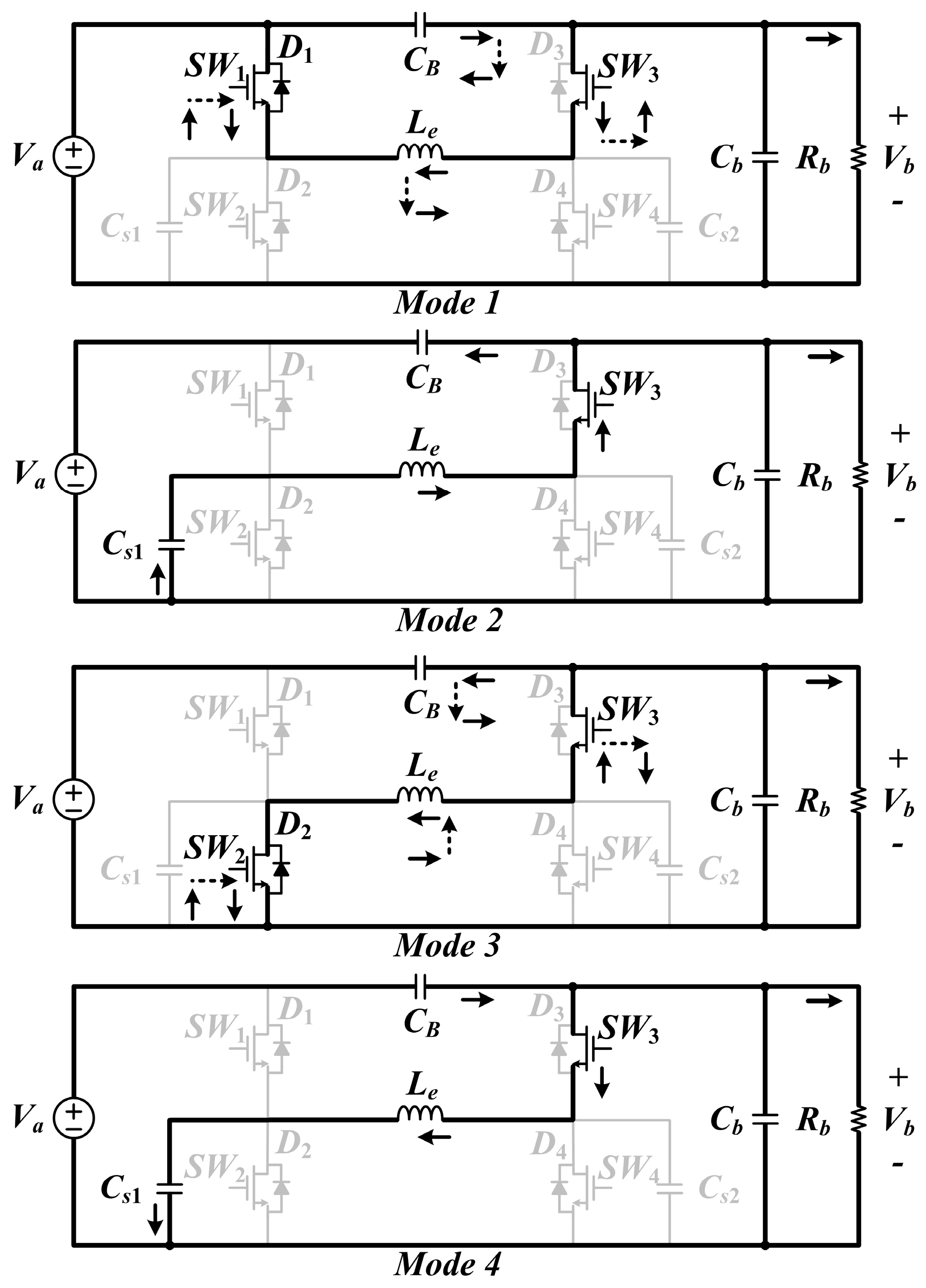
To improve the aforementioned drawbacks of the existing converters, this paper proposes a CBB BDC circuit structure that is suitable for use in ESS for distributed generation. The proposed CBB BDC (
Figure 5) uses the CBB BDC circuit in [
10] as a basic structure, reduces the core loss by using a 1:1 transformer, decreases switching losses by using two small snubber capacitors
Cs1 and
Cs2, and reduces filter size by using a dc-blocking capacitor
CB. Unlike the converter of [
15], the proposed converter can have a MPPT range of 0 <
VPV <
VOC, regardless of
Vbat (
Figure 4b), because the proposed CBB BDC works well for both
VIN >
VO and
VIN ≤
VO. Therefore, the proposed circuit is suitable for PV–ESS, which requires high efficiency in the condition of overlapping input and output range. The circuit is controlled using pulse-frequency modulation (PFM) combined with pulse-width modulation (PWM), the load variation is accommodated using PFM, and the voltage gain is adjusted using PWM. The circuit structure, principle of operation, and design considerations of the proposed circuit are described in
Section 2. A digital controller is given in
Section 3. Experimental results are given in
Section 4. Conclusions are given in
Section 5.
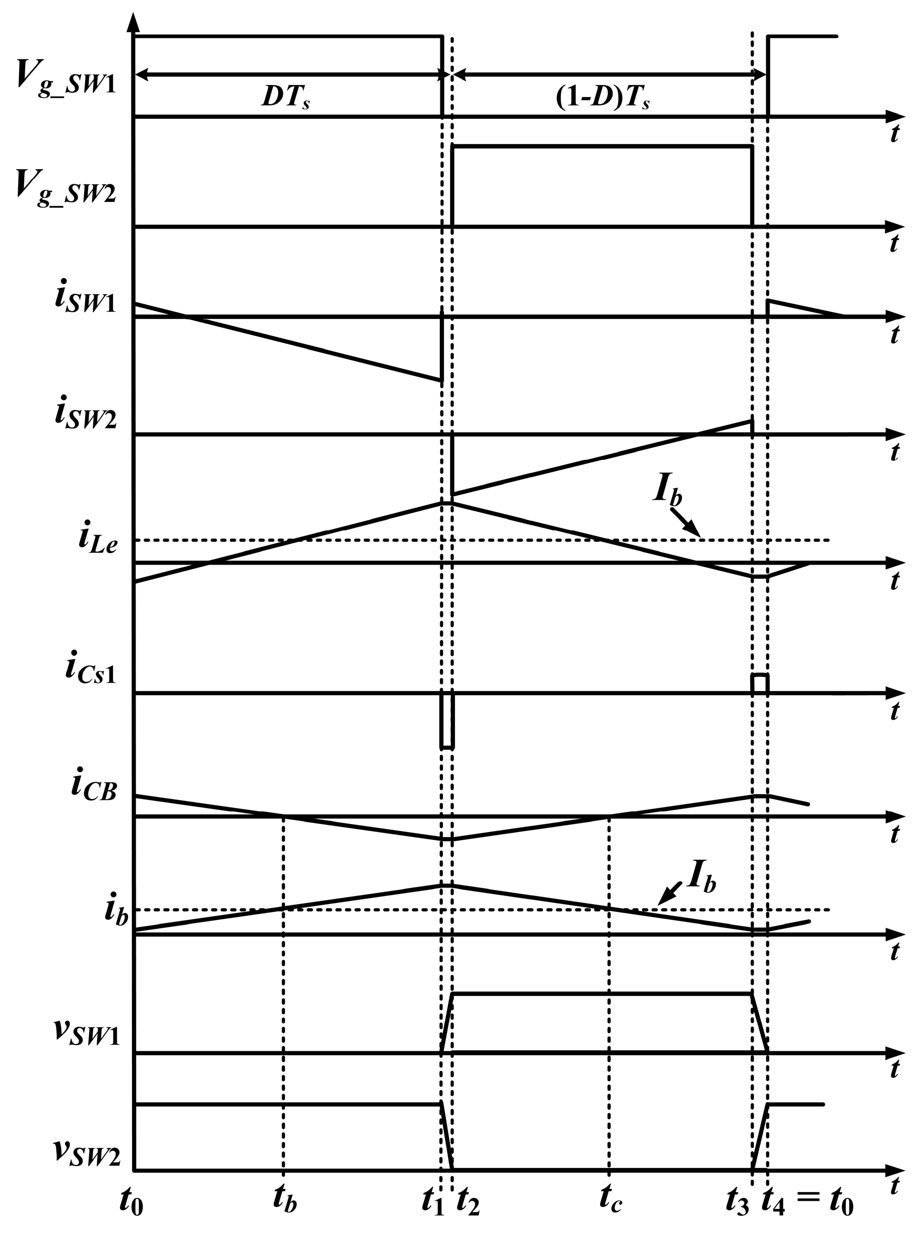
3. Digital Controller
The control circuit (
Figure 11) was implemented on a digital signal processor (DSP, TMS320F28335, Texas Instruments). The circuit controls the direction of energy transfer: Forward (Flag_ConStart = 1, D_mode = 1,
Va →
Vb) and backward (Flag_ConStart = 1, D_mode = 0,
Vb →
Va) directions. The circuit also determines switching duties
DSW1–
DSW4 for
SW1–
SW4 such that
DSW1 = 1,
DSW2 = 0,
DSW3 = 1 –
D, and
DSW4 =
D for
Va <
Vb; and
DSW1 =
D,
DSW2 = 1 –
D,
DSW3 = 1, and
DSW4 = 0 for
Va >
Vb. The inputs to the circuit are
Va,
Ia,
Vb,
Ib, two reference voltages
Va,ref and
Vb,ref, two limit voltages
Va,lim and
Vb,lim, two limit currents
Ia,lim and
Ib,lim, and a reference duty
Dref. The proportional-integral (PI) controller set
VPI,ref =
Vb,ref and
VPI =
Vb for forward-conversion, or
VPI,ref =
Va,ref and
VPI =
Va for backward-conversion. The PI controller calculates the error
VPI,ref -
VPI and produces the PI output
U[
n]. Then, after
D[
n] =
U[
n]+
Dref is calculated,
D[
n] is multiplied by the switching period
Ts[
n] to produce a PWM reference duty
Ref[
n];
Ref[
n] is the non-inverting input to the comparator that adjusts
D to keep the voltage gain constant.
The PFM controller calculates the switching period
Ts[
n] =
Ts,min + K
|Ia|/
Ia,max (where
K is a constant,
Ts,min is the lowest switching period, and
Ia,max is the highest value of
Ia), then resets the 16-bit counter when the counter output
Tc(
j) =
Ts[
n]. The converter must operate at 110 kHz ≤
fs ≤ 330 kHz, so the range of
Ts[
n] was determined as 454 ≤
Ts[
n] ≤ 1363 for the clock frequency of the counter
fclk = 150 MHz. As the ratio
Vb/
Va increases,
fs that ensures ZVS under full load decreases for the buck conversion but increases for the boost conversion. Therefore,
for buck conversion and
for boost conversion, where
β is a constant to adjust the slope of the frequency change (
Dmin = 0.15,
Dmax = 0.85, and
β = 1 for buck- or boost-mode control).
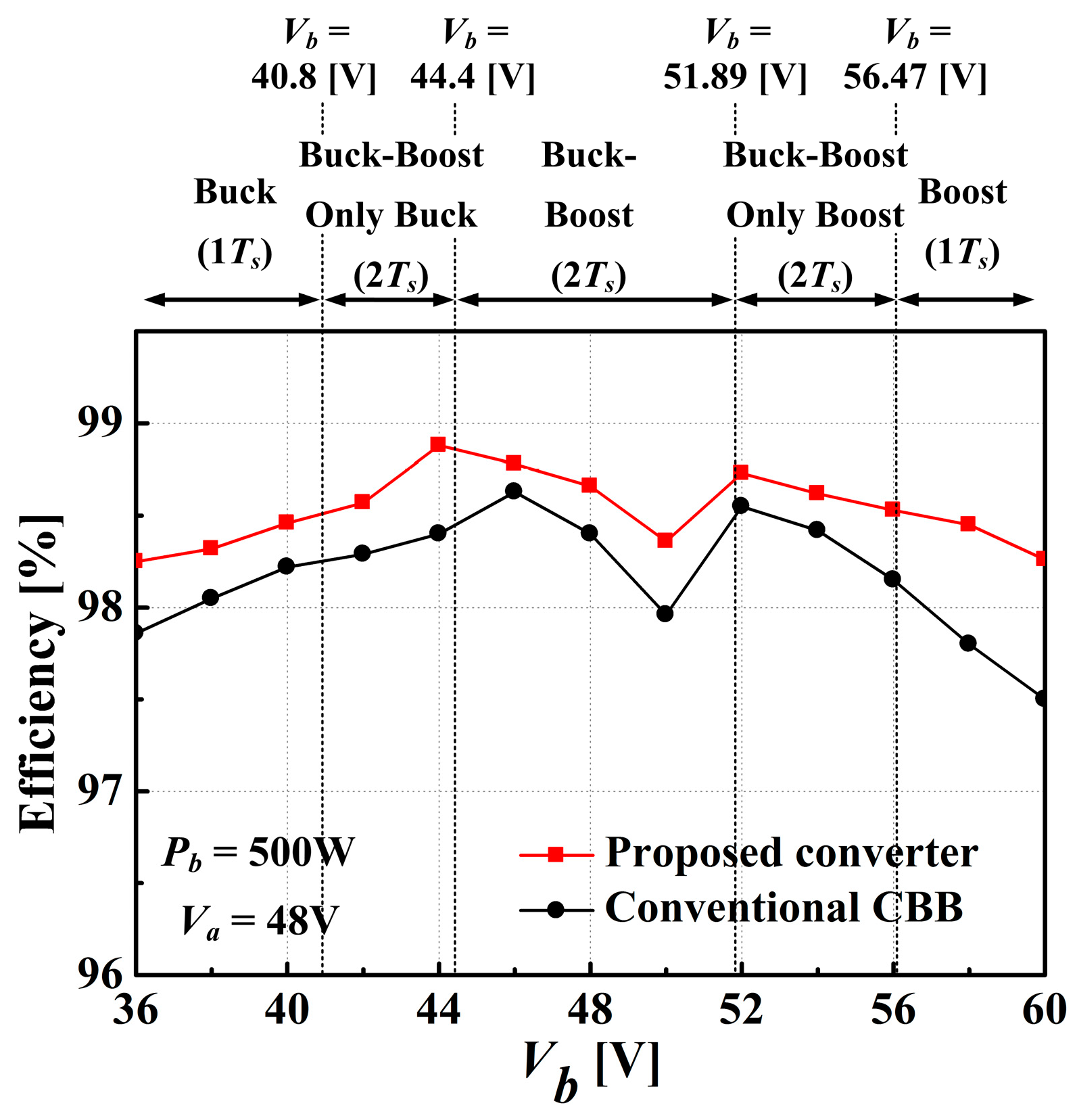
When Vb/Va is close to 1, the dead time prevents the converter from regulating the output voltage properly by using only buck-mode or boost-mode control. This problem was solved using a buck- and boost-mode alternating control either when D for buck mode conversion (Dbuck) becomes >0.85, or when D for boost mode conversion (Dboost) becomes <0.15; the converter assumes Va = 48 V, so it uses this buck–boost mode control for 40.8 V ≤ Vb ≤ 56.5 V. Under the buck–boost mode control, the volt-second balance for two switching periods yields
The ripple current of for the buck–boost control increases as Dboost increases or as Dbuck decreases. To have high ηe, Dboost should be minimized and Dbuck should be maximized. The converter sets Dboost = 0 but adjusts Dbuck from 0.7 to 0.85 for 40.8 V ≤ Vb ≤ 44.4 V, sets Dbuck = 1, but adjusts Dboost from 0.15 to 0.31 for 51.89 V ≤ Vb ≤ 56.47 V, and sets Dbuck = 0.75 but adjusts Dboost from 0.1 to 0.39 for 44.4 V < Vb < 51.89 V. The values of β were chosen as 1.1 for 40.8 V ≤ Vb ≤ 44.4 V, as 1.9 for 44.4 V < Vb < 51.89 V, and as 1.4 for 51.89 V ≤ Vb ≤ 56.47 V.
The comparator output becomes “high” whenever Tc(j) = Ts[n]; this produces the switching time-period Ts = Ts(n)/fclk. The comparator output becomes “low” when Ref[n] < Tc(j). The Flip/Flops and dead-time generator emit inverting and non-inverting gate signals for the switches.
4. Experimental Results
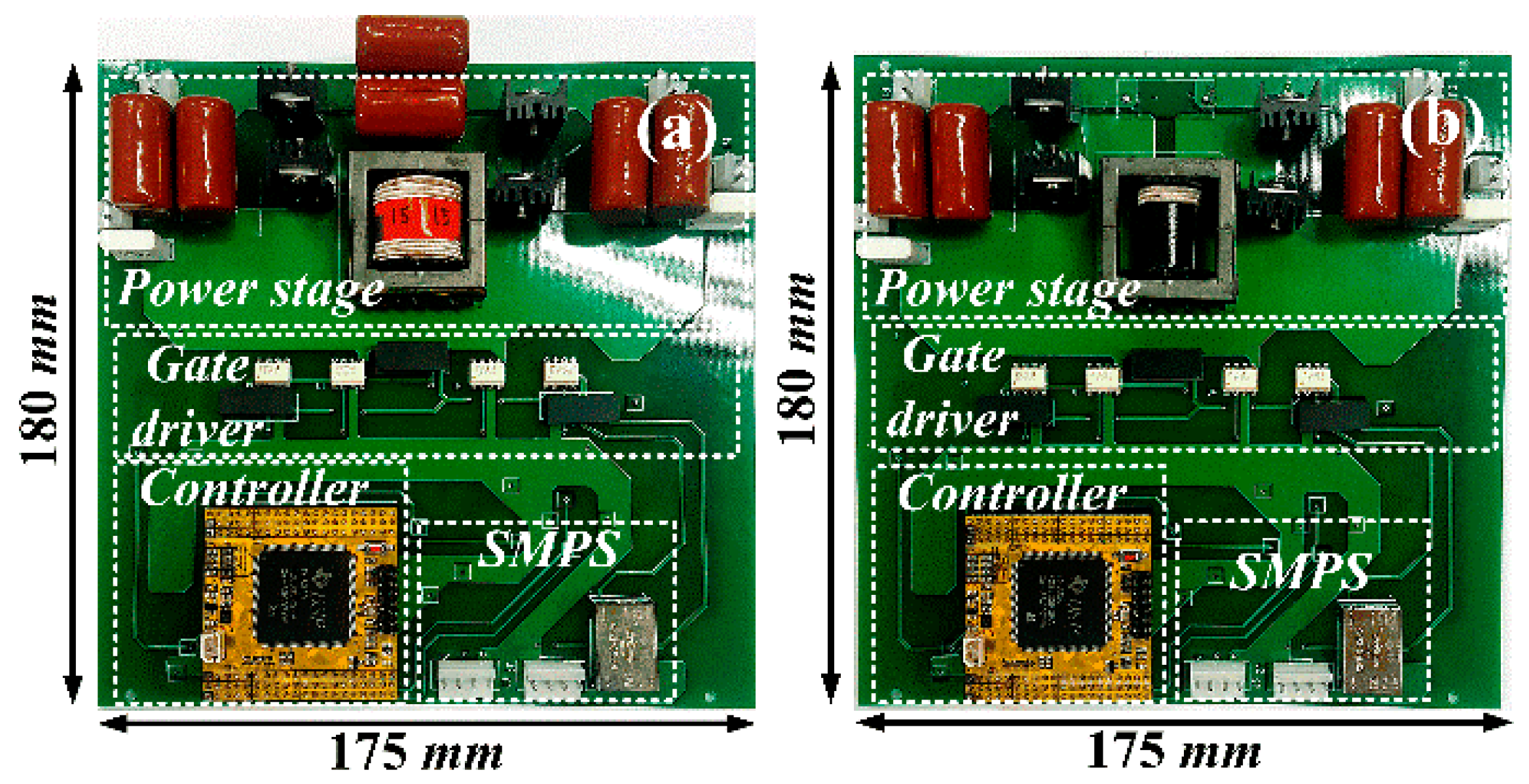
The proposed CBB BDC (
Figure 12a) was fabricated using the chosen parameters (
Table 3). It was designed to operate at
Va = 48 V, 0.15 ≤
D ≤ 0.85, 36 V ≤
Vb ≤ 60 V, 40 kHz ≤
fs ≤ 210 kHz, 1.04 A ≤
Ia ≤ 10.4 A and 0.83 A ≤
Ib ≤ 13.9 A. The PI coefficients of the controller were optimized to
kp = 0.02 and
ki = 0.2. The sampling frequency for analog signals was 20 kHz, and the analog-to-digital converter had 12-bit resolution. When
Pb increased from 50 to 500 W,
fs decreased from 210 to 40 kHz during buck conversion and from 201 to 64 kHz during boost conversion. The dead time for switch control was 110 ns. The switching devices were the IPP200N15N3 power MOSFETs (Infineon).
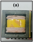
The 1:1 transformer was fabricated using an ETD 34 ferrite core with
N = 15, as discussed in
Section 2.5. For comparison, the conventional CBB BDC in [
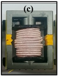
10] (
Figure 12b) was also fabricated using the IPP200N15N3 power MOSFETs and three different inductors with
L =
Llk/2 = 5.25 μH (
Table 4). Inductor 1 used an ETD 34 ferrite core and had an air-gap length
Sa = 0.1 mm, which resulted in
L = 5.25 μH when
N = 3. This inductor had core saturation at high power operation. Inductor 2 used the same core, but increased
Sa to 8 mm to prevent core saturation, which resulted in
L = 5.25 μH when
N = 15. Inductor 3 had
N = 3 and
Sa = 0.1 mm but prevented core saturation by increasing the core size. The filter capacitors for the conventional CBB BDC were
Ca =
Cb = 40 μF.
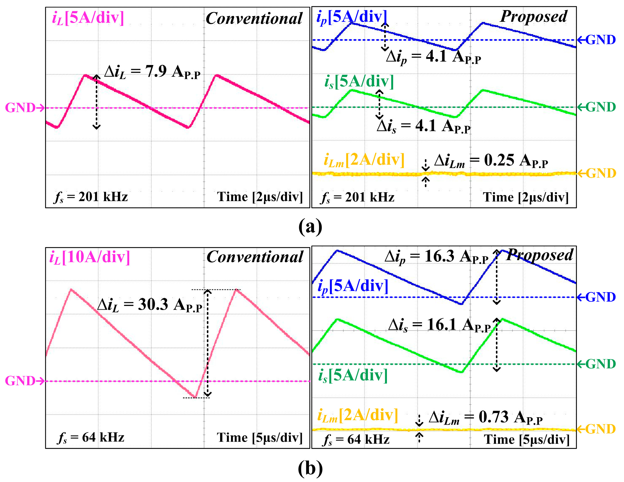
The waveforms of
,
,
, and
for forward boost conversion (
Figure 13) were measured at
Va = 48 V,
Vb = 60 V,
Pb = 50 W or
Pb = 500 W. The proposed converter operated in PFM and had
A
p-p for
Pb = 50 W (
Figure 13a) and ≤16.3 A
p-p for
Pb = 500 W (
Figure 13b).
was 0.25 A
p-p at
Pb = 50 W and 0.73 A
p-p at
Pb = 500 W, when
was calculated using the
is and
ip measurements. The conventional CBB BDC operated at
fs = 64 kHz and had an inductor current ripple
= 30.3 A
p-p at
Pb = 500 W.
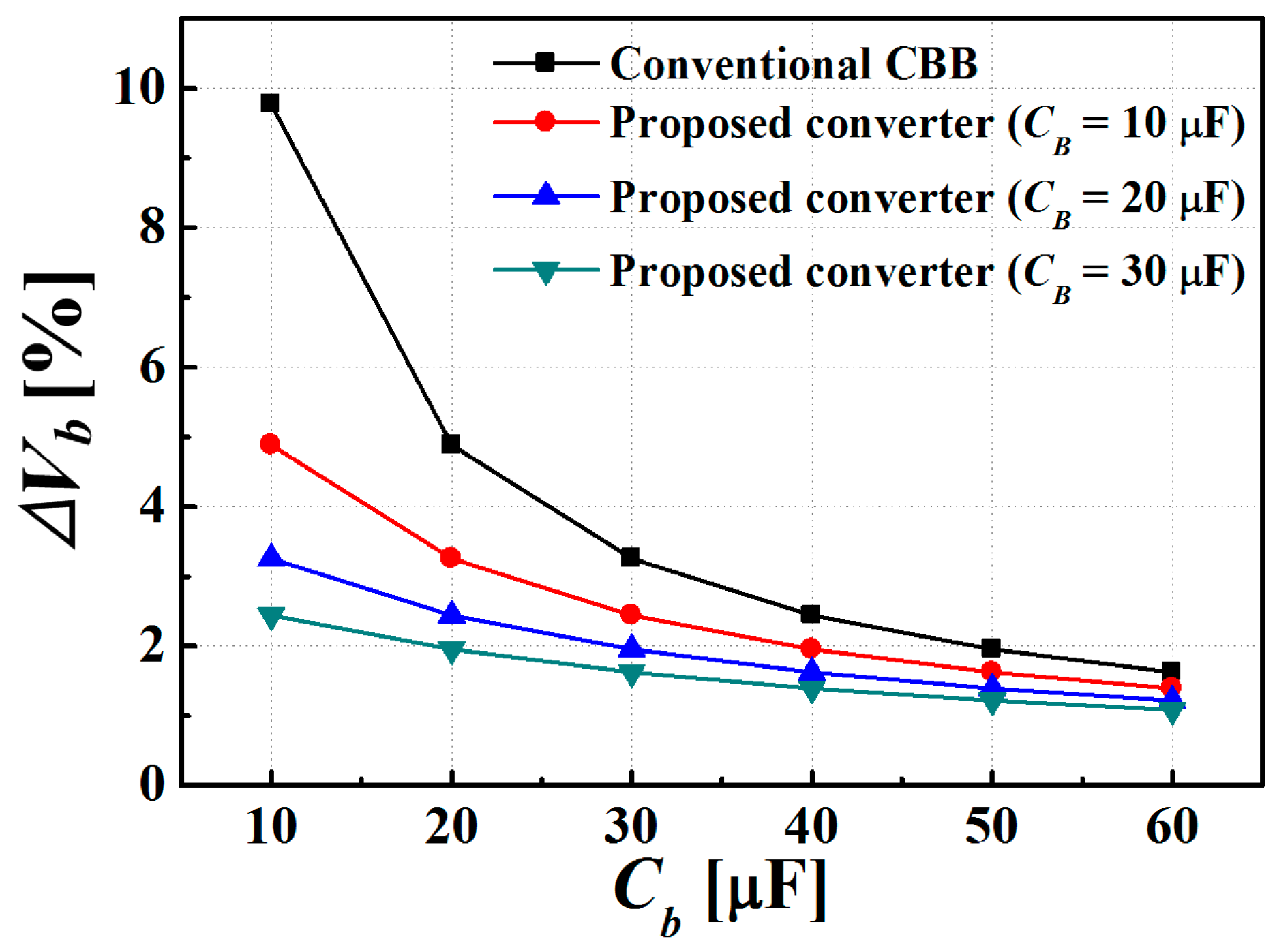
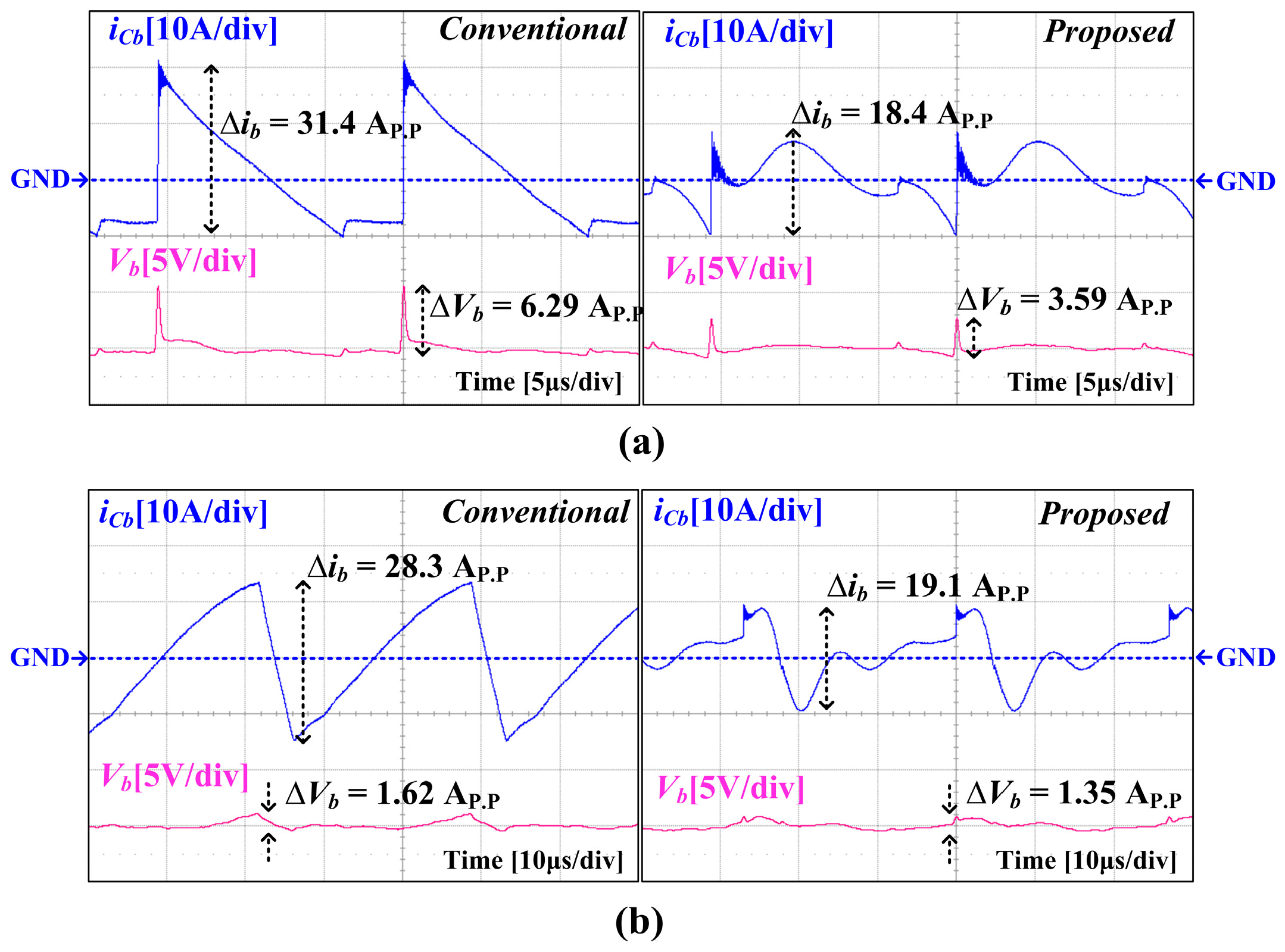
The waveforms of
and Δ
Vb (
Figure 14) were measured at
Va = 48 V and
Pb = 500 W, while the converters were operated at
Vb = 60 V (boost conversion,
Figure 14a) or
Vb = 36 V (buck conversion,
Figure 14b). Δ
Vb for boost conversion to
Vb = 60 V was 3.59 V
p.p for the proposed and 6.29 V
p.p for the conventional CBB BDCs. Δ
Vb for buck conversion to
Vb = 36 V was 1.35 V
p.p for the proposed and 1.62 V
p.p for the conventional CBB BDCs. Considering that
Ca =
Cb =
CB = 20 μF in the proposed converter and
Ca =
Cb = 40 μF in the conventional CBB BDC, the proposed converter reduced the total capacitance by 20 μF for the given Δ
Vb, by providing a bypass to
iLe through
CB.
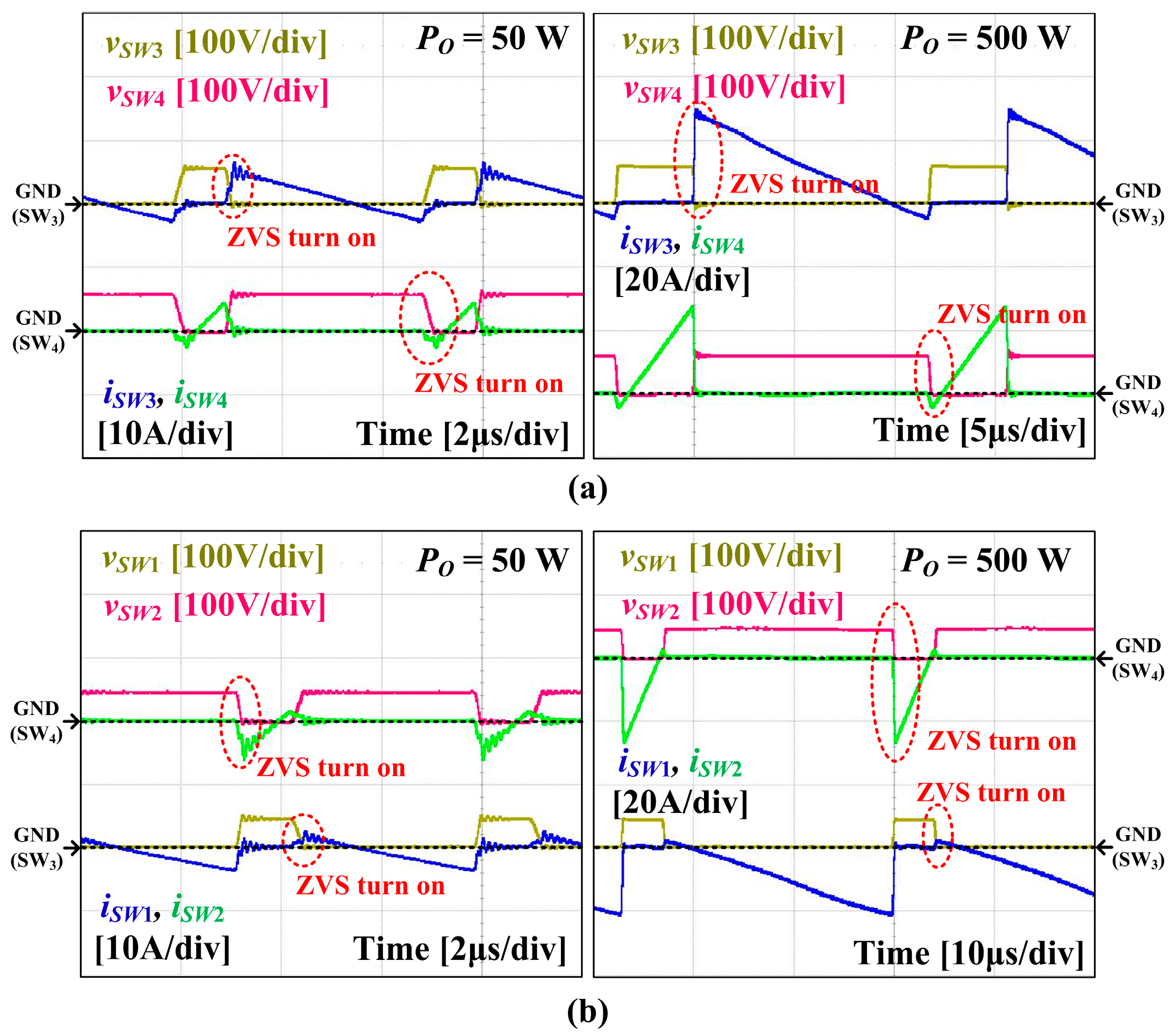
The current and voltage waveforms of switches in the proposed converter for
Va = 48 V (
Figure 15) were measured at
Pb = 50 W and 500 W, while the converter was operated in either boost (
Vb = 60 V,
Figure 15a) or buck (
Vb = 36 V,
Figure 15b) mode. These waveforms show: 1)
> 0 when
SW4 was turned off; 2)
increased only up to
Vb; 3) 1) and 2) indicate that the body diode of
SW3 was turned on when
SW4 was turned off, so
SW3 had ZVS turn-on; 4)
< 0 when
SW3 was turned off; 5)
increased only up to
Vb; 6) 4) and 5) indicate that the body diode of
SW4 was turned on when
SW3 was turned off, so
SW4 had ZVS turn-on. The waveforms in
Figure 15b show: 7)
< 0 when
SW1 was turned off; 8)
increased only up to
Va; 9) points 7) and 8) indicate that the body diode of
SW2 was turned on when
SW1 was turned off, so
SW2 had ZVS turn-on; 10)
> 0 when
SW2 was turned off; 11)
increased only up to
Va; 12) points 10) and 11) indicate that the body diode of
SW1 was turned on when
SW2 was turned off, so
SW1 had ZVS turn-on; 13)
fs increased as
Pb decreased; this result shows that PFM worked properly and the currents of switches were decreased by the reduced
and
at the light load; and 14) PWM adjusted
D of the main switch so that
Vb followed the reference voltage.
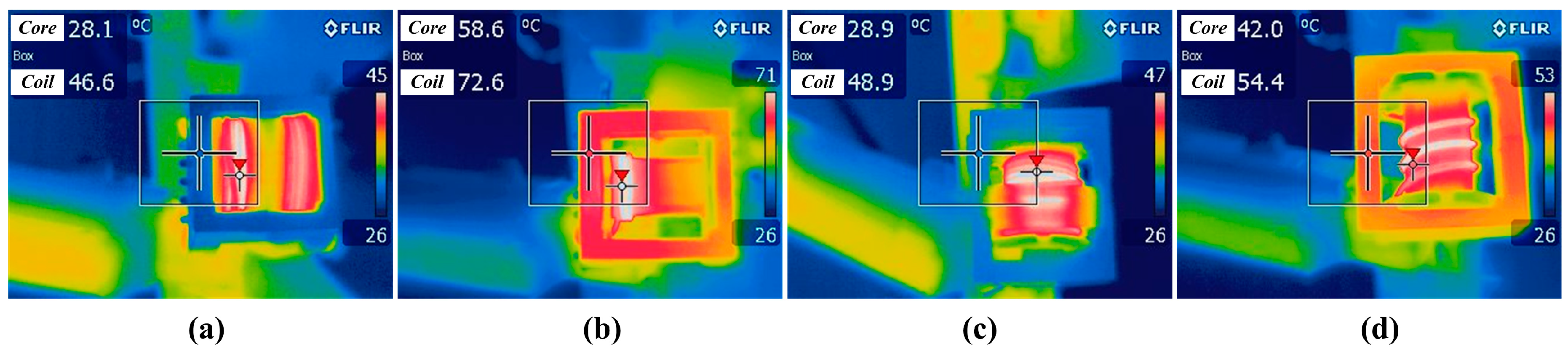
The temperatures of cores and windings (
Figure 16) were measured at
Va = 48 V,
Vb = 60 V, and
Pb = 500 W. The proposed converter had small core loss because
iLm was reduced significantly by connecting the windings of the transformer in parallel and in inverse-coupling configuration. As a result, the core temperature
Tcore = 28.1 °C and the winding temperature
Twinding = 46.6 °C of the proposed converter (
Figure 16a) were lower than the other conventional CBB BDCs:
Tcore = 58.6 °C and
Twinding = 72.6 °C for inductor 1 at
Pb = 350 W (
Figure 16b),
Tcore = 28.9 °C and
Twinding = 48.9 °C for inductor 2 at
Pb = 500 W (
Figure 16c), and
Tcore = 42.0 °C and
Twinding = 54.4 °C for inductor 3 at
Pb = 500 W (
Figure 16d). Note that the conventional converter could not operate for
Pb > 350 W due to core saturation, so the temperature was measured at 350 W.
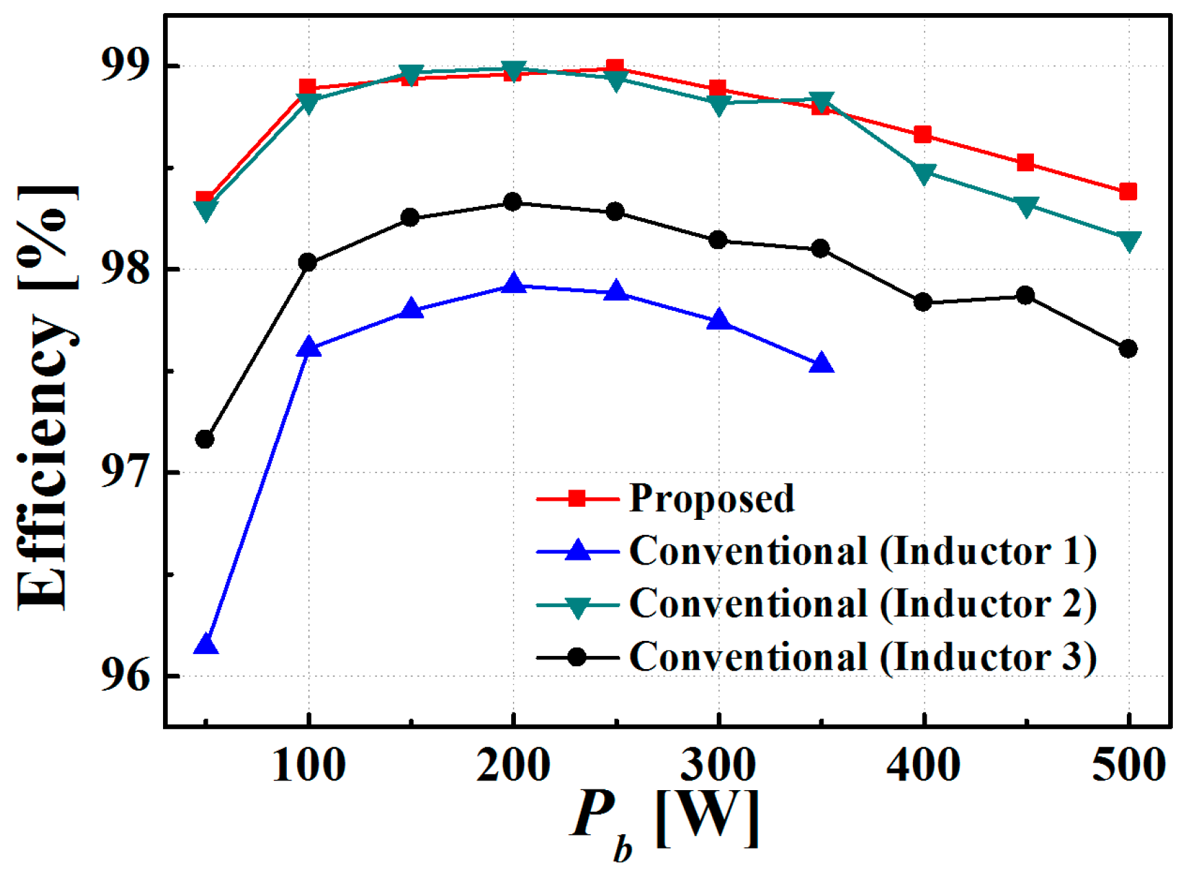
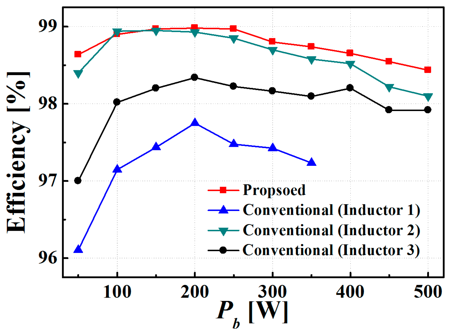
ηe vs.
Pb (
Figure 17) for boost conversion were measured at
Va = 48 V and
Vb = 60 V, while the converters were operated in PFM mode (64 kHz ≤
fs ≤ 210 kHz).
ηe of the proposed converter was ≥98.3% for
Pb > 50 W. The conventional CBB BDC using inductor 1 could not operate at
Pb > 350 W due to core saturation; this converter had
ηe = 96.1% at
Pb = 50 W and
ηe = 97.5% at
Pb = 350 W when operated in PFM mode. After replacing inductor 1 with inductor 2, the converter had
ηe = 98.3% at
Pb = 50 W and
ηe = 98.1% at
Pb = 500 W, which are very close to that for the proposed converter. However, inductor 2 has a large air gap and is difficult to fabricate. Fabrication of the converter using inductor 3 yielded
ηe = 97.2% at
Pb = 50 W and
ηe = 97.6% at
Pb = 500 W. The core and switching losses were reduced in the proposed converter, so it had higher
ηe than the conventional CBB BDCs. The behaviors of
ηe vs.
Pb for buck conversion at
Va = 48 V,
Vb = 36 V, and 64 kHz ≤
fs ≤ 201 kHz (
Figure 18) were quite similar to those for boost conversion.
ηe vs.
Vb (
Figure 19) was measured at
Va = 48 V and
Pb = 500 W. The proposed converter had
ηe ≥ 98.3% for 36 V ≤
Vb ≤ 60 V, whereas the conventional CBB BDC had ~0.76% lower
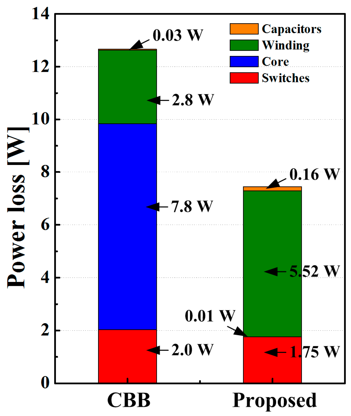
ηe than the proposed converter. The results of loss analyses at
Va = 48 V,
Vb = 60 V, and
Pb = 500 W show that the total losses were 7.41 W in the proposed circuit and 12.6 W in the conventional CBB BDC (
Figure 20). The major losses in the proposed converter were the switching (1.75 W) and winding (5.52 W) losses, and those in the conventional CBB BDC were the core (7.8 W), switching (2.0 W), and winding (2.8 W) losses. In the proposed converter, the switching loss was reduced by using the snubber capacitors C
s1 and C
s2, and the core loss was reduced significantly by connecting the windings of the 1:1 transformer in parallel and in inverse-coupling configuration, but the winding loss was increased because
N was increased.
The costs of the conventional and proposed CBB BDCs were calculated using the prices on the websites of [
23] and [
24] (
Table 5), assuming that both BDCs use the same switches and ferrite core and have the same input/output voltage ripples. Compared to the conventional converter, the proposed CBB BDC costs
$1.93 more because
CB,
Cs1,
Cs2 and transformer windings are additionally required. However, the proposed CBB BDC can save
$14.44 in cost by using small filter capacitors. Therefore, the proposed CBB BDC is
$5.29 cheaper than the conventional one.

 ,
, 


