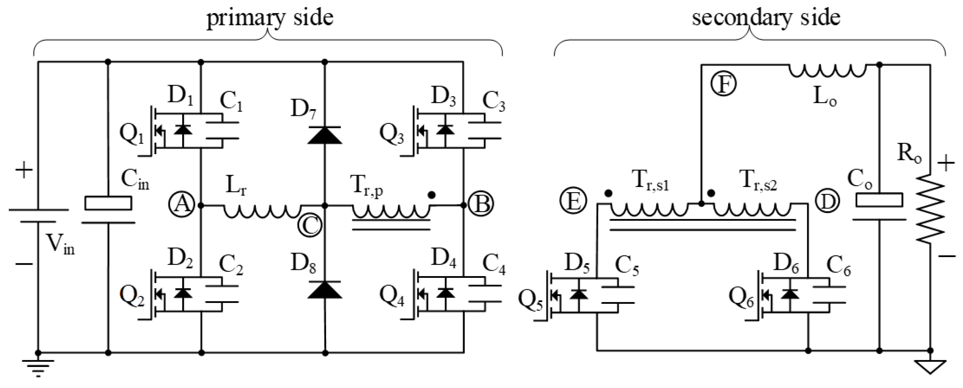
Figure 1.
Phase shift full bridge (PSFB) converter with center tapped rectification stage, external resonant inductance and clamping diodes.
Figure 1.
Phase shift full bridge (PSFB) converter with center tapped rectification stage, external resonant inductance and clamping diodes.
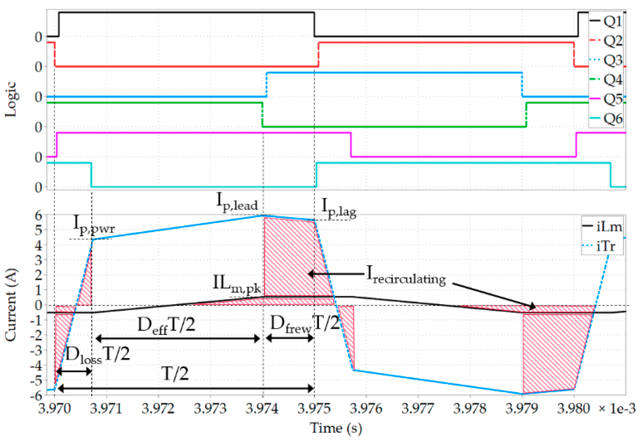
Figure 2.
Primary side current and PWM control signals of a simplified model of a PSFB converter.
Figure 2.
Primary side current and PWM control signals of a simplified model of a PSFB converter.
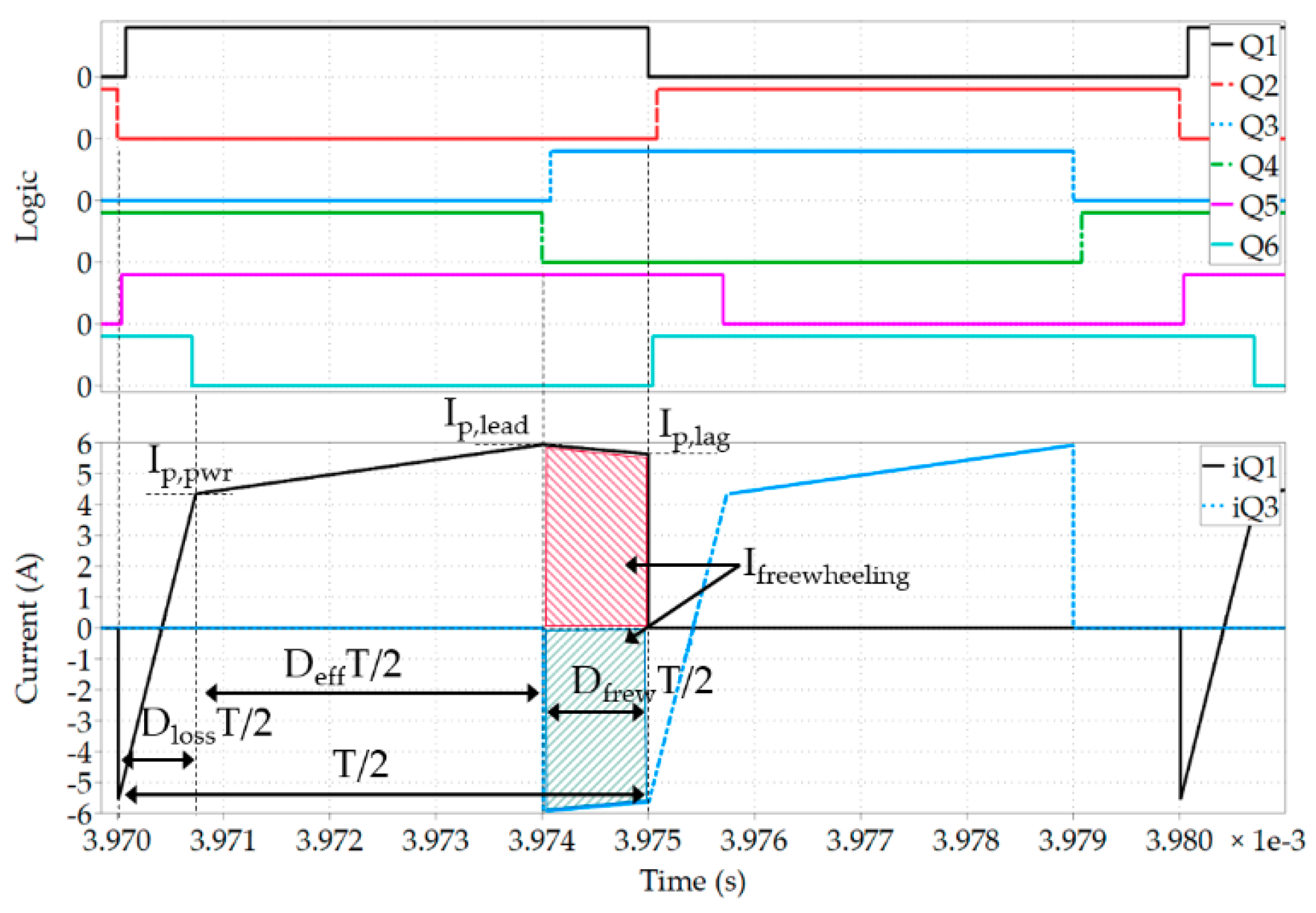
Figure 3.
Primary side HV MOSFETs current and PWM control signals of a simplified model of a PSFB converter.
Figure 3.
Primary side HV MOSFETs current and PWM control signals of a simplified model of a PSFB converter.
Figure 4.
Secondary side LV MOSFETs current and PWM control signals of a simplified model of a PSFB converter.
Figure 4.
Secondary side LV MOSFETs current and PWM control signals of a simplified model of a PSFB converter.
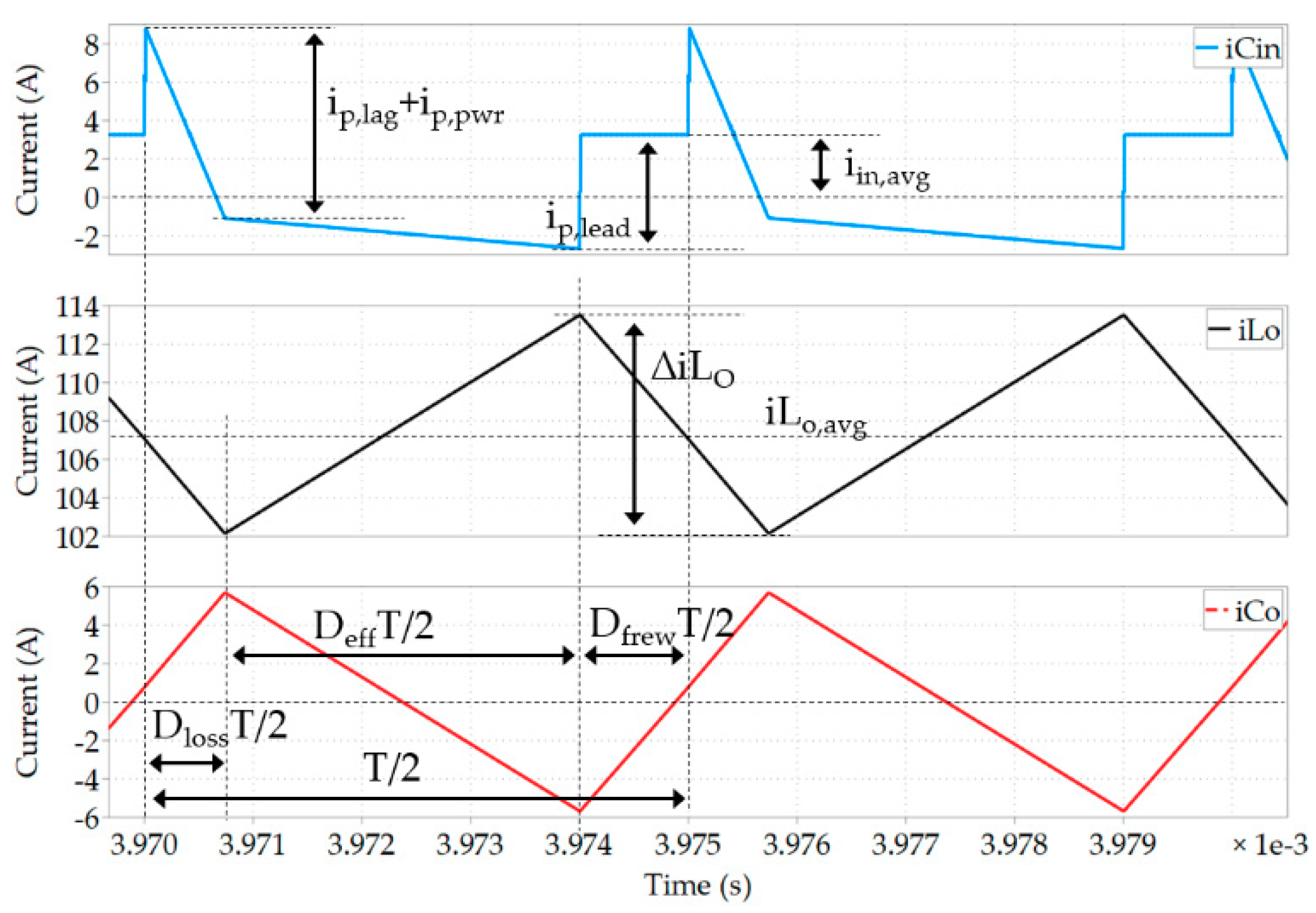
Figure 5.
Input capacitor, output choke and output capacitor currents of a simplified model of a PSFB converter.
Figure 5.
Input capacitor, output choke and output capacitor currents of a simplified model of a PSFB converter.
Figure 6.
Efficiency for different clamping diodes’ configuration and the effect on switching voltage of the primary side HV MOSFETs and the primary side circulating currents: (a) differential efficiencies; (b) differential losses; (c) leading and lagging leg switching voltages with the clamping diodes on the lagging leg position; (d) leading and lagging leg switching voltages with the clamping diodes on the leading leg position; (e) primary side and clamping diodes current with clamping diodes in the lagging leg; (f) primary side and clamping diodes current with clamping diodes in the leading leg.
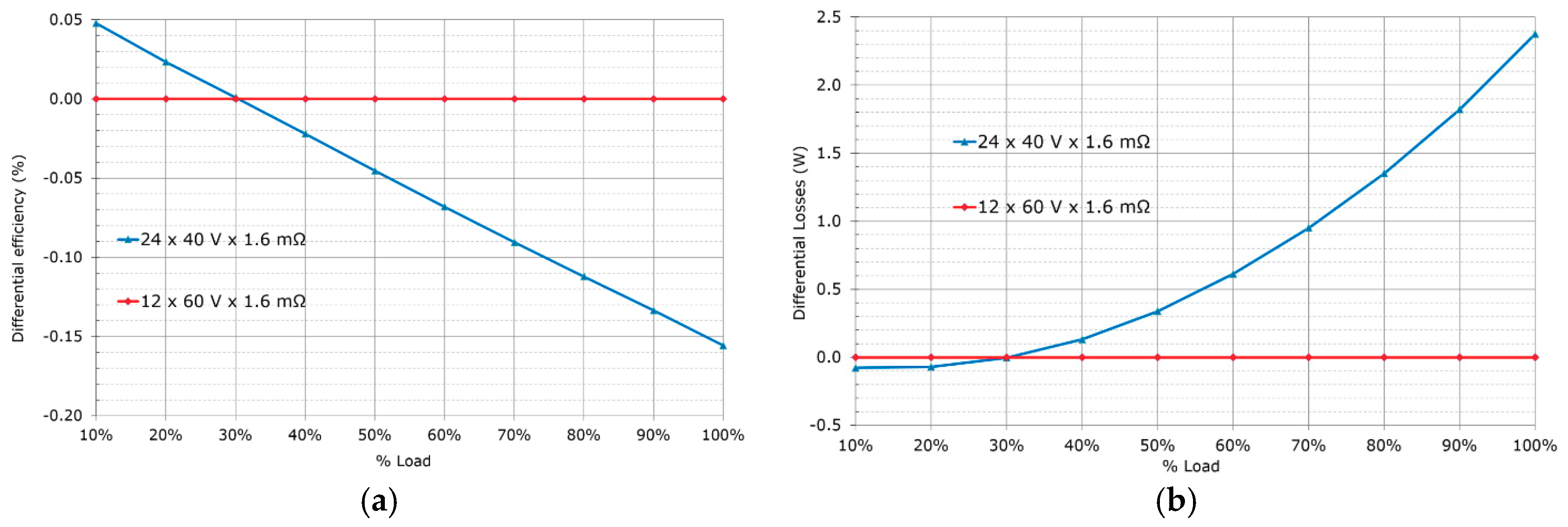
Figure 7.
Performance comparison for different rectification stage configuration of equivalent RDS(on). Full bridge rectification with 24 units of 40 V class devices in blue, and the center tapped with 12 units of 60 V class devices in red. (a) Differential efficiency; (b) differential losses.
Figure 7.
Performance comparison for different rectification stage configuration of equivalent RDS(on). Full bridge rectification with 24 units of 40 V class devices in blue, and the center tapped with 12 units of 60 V class devices in red. (a) Differential efficiency; (b) differential losses.
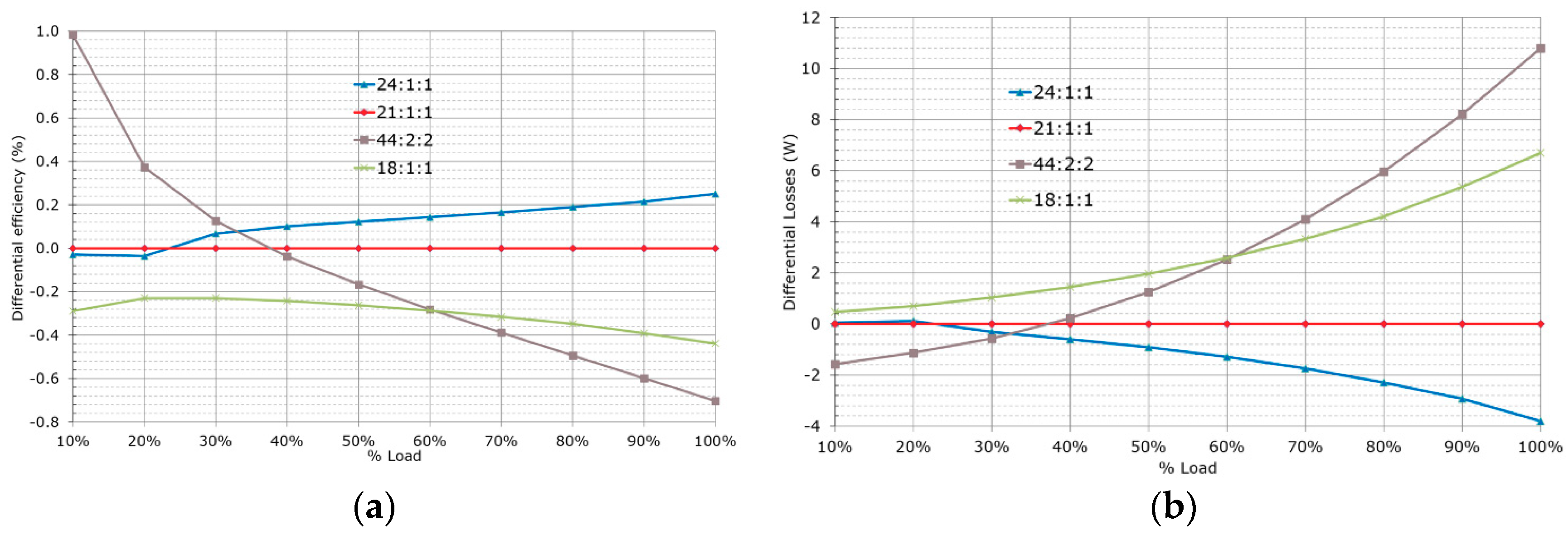
Figure 8.
Performance comparison for different transformer turns ratios. The value of Lr is adjusted to maintain the required input voltage range. The original reference converter had a turn ratio of 44:2:2. The optimized converter has a turn ratio of 21:1:1. (a) Differential efficiency of the converter with the different configurations; (b) differential power loss of the converter with the different configurations.
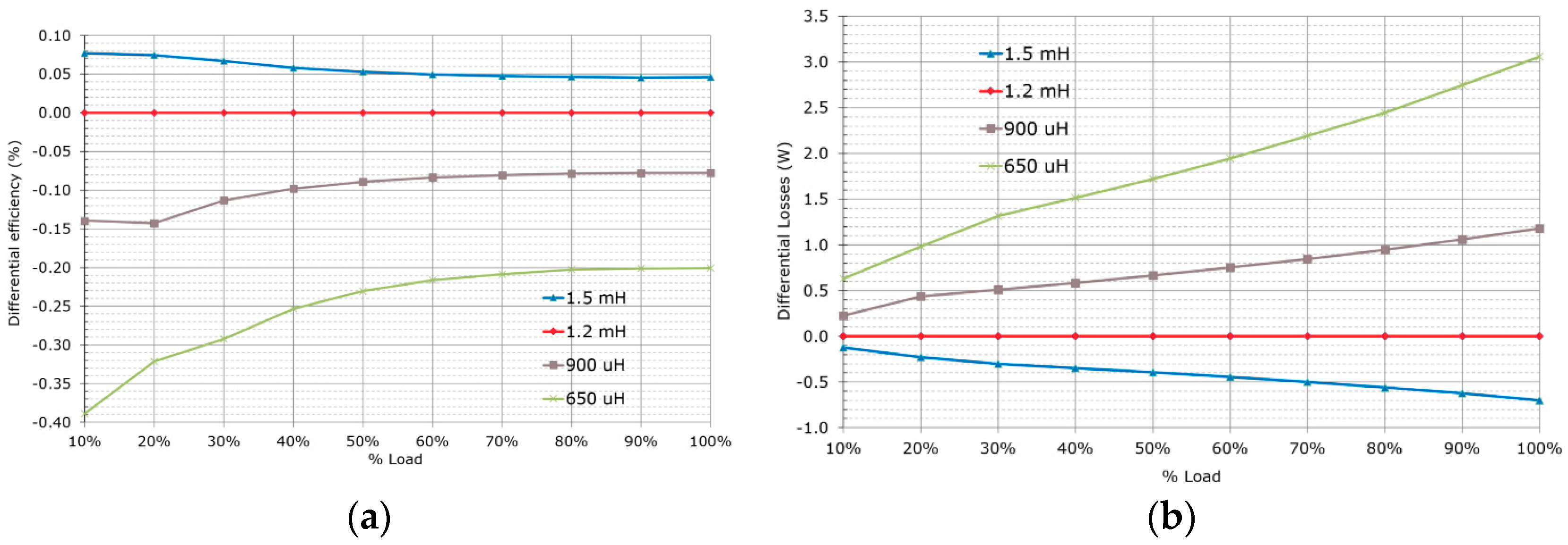
Figure 9.
Performance comparison for different magnetizing inductances: (a) differential efficiency; (b) differential losses.
Figure 9.
Performance comparison for different magnetizing inductances: (a) differential efficiency; (b) differential losses.
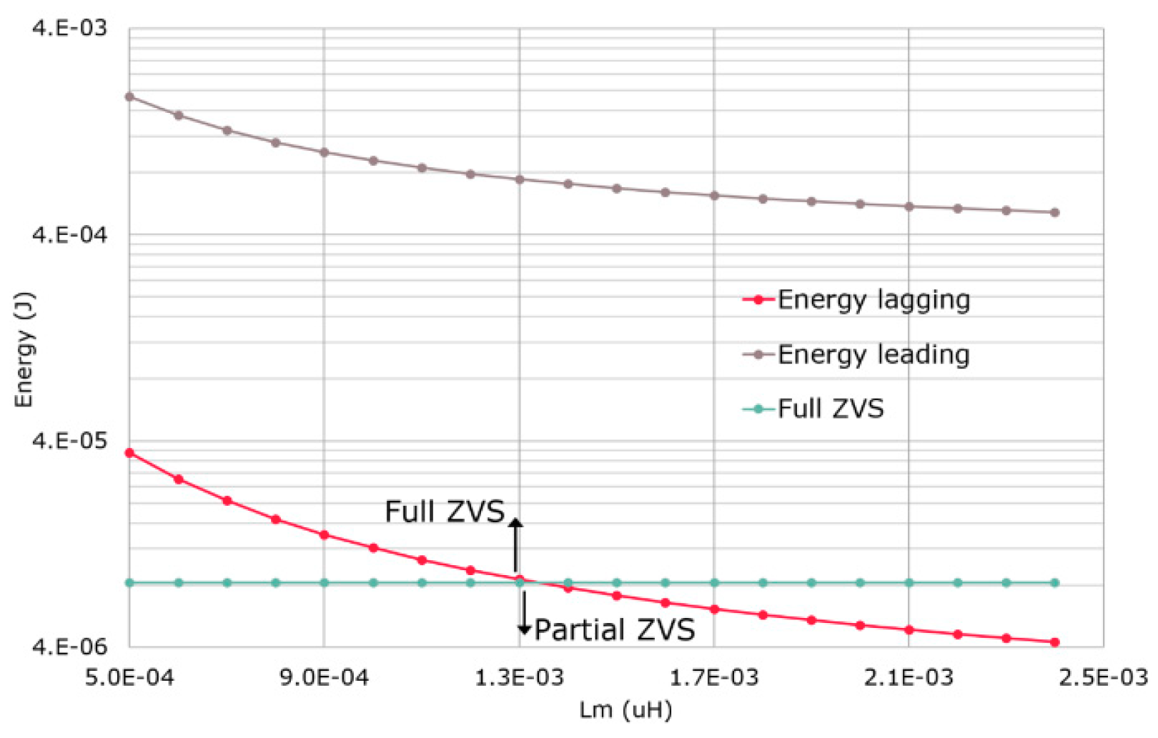
Figure 10.
Available energy for the zero-voltage-switiching (ZVS) transitions depending on the value of the magnetizing inductance with the converter operating at 10% of the load.
Figure 10.
Available energy for the zero-voltage-switiching (ZVS) transitions depending on the value of the magnetizing inductance with the converter operating at 10% of the load.
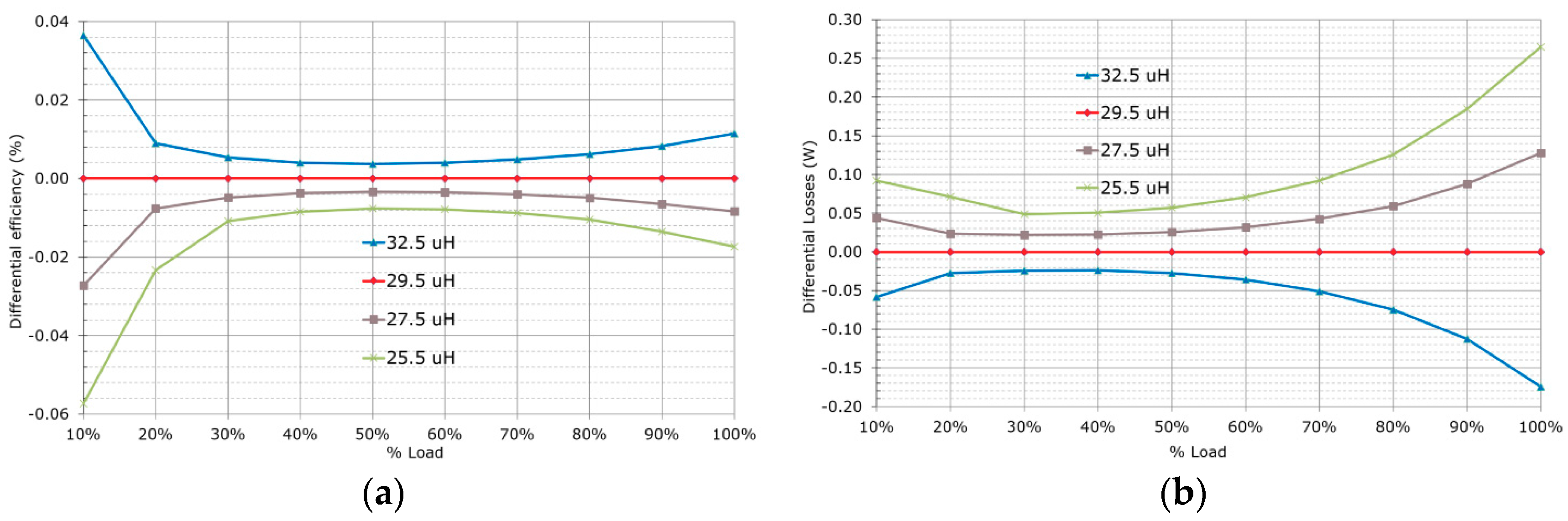
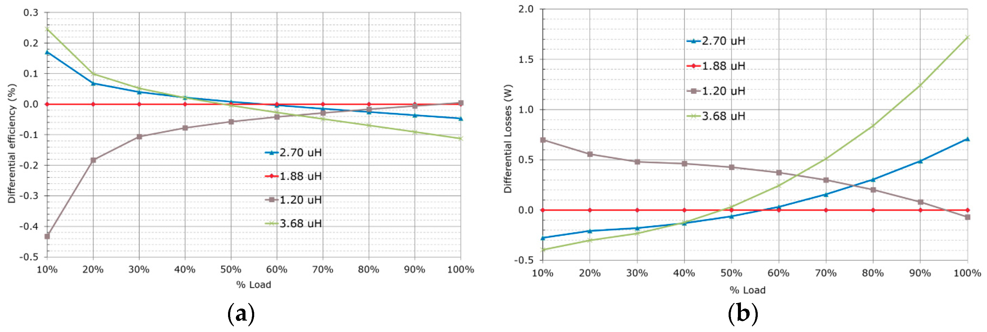
Figure 11.
Performance comparison for different external resonant inductances: (a) differential efficiency; (b) differential losses.
Figure 11.
Performance comparison for different external resonant inductances: (a) differential efficiency; (b) differential losses.
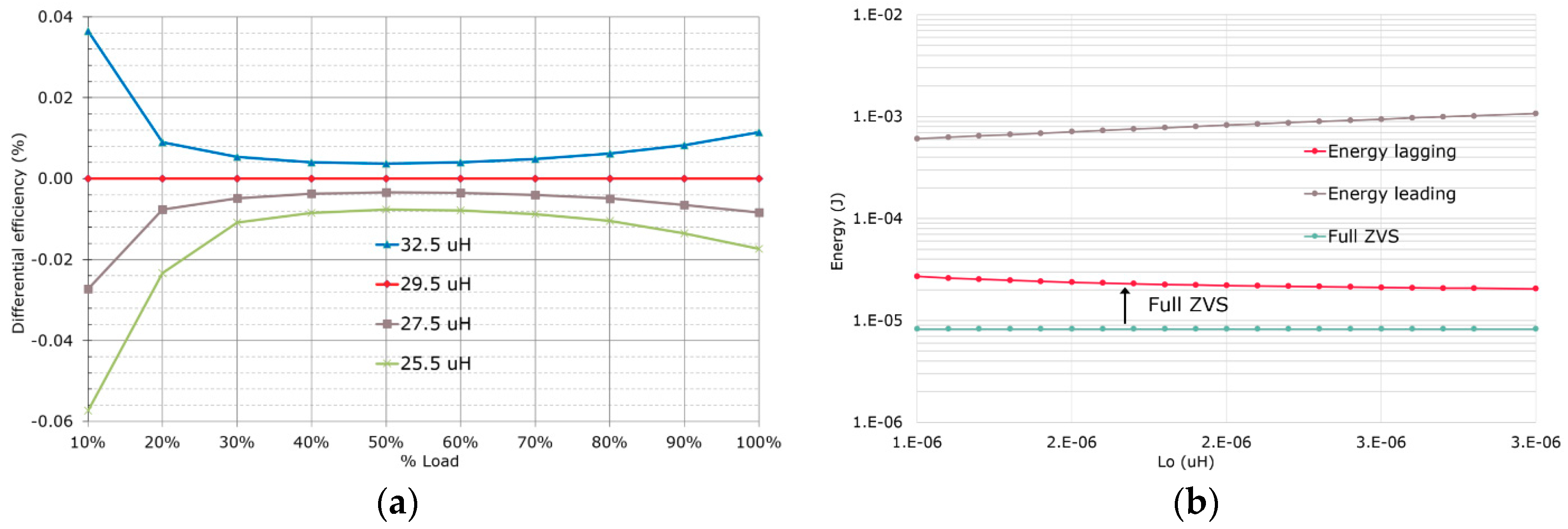
Figure 12.
Available energy for the ZVS transitions depending on the value of the output inductor Lo at 10% of the load. (a) Simplified model without clamping diodes; (b) with primary side clamping diodes in the lagging leg.
Figure 12.
Available energy for the ZVS transitions depending on the value of the output inductor Lo at 10% of the load. (a) Simplified model without clamping diodes; (b) with primary side clamping diodes in the lagging leg.
Figure 13.
Performance comparison for different numbers of turns of the output inductor: (a) differential efficiency; (b) differential losses.
Figure 13.
Performance comparison for different numbers of turns of the output inductor: (a) differential efficiency; (b) differential losses.
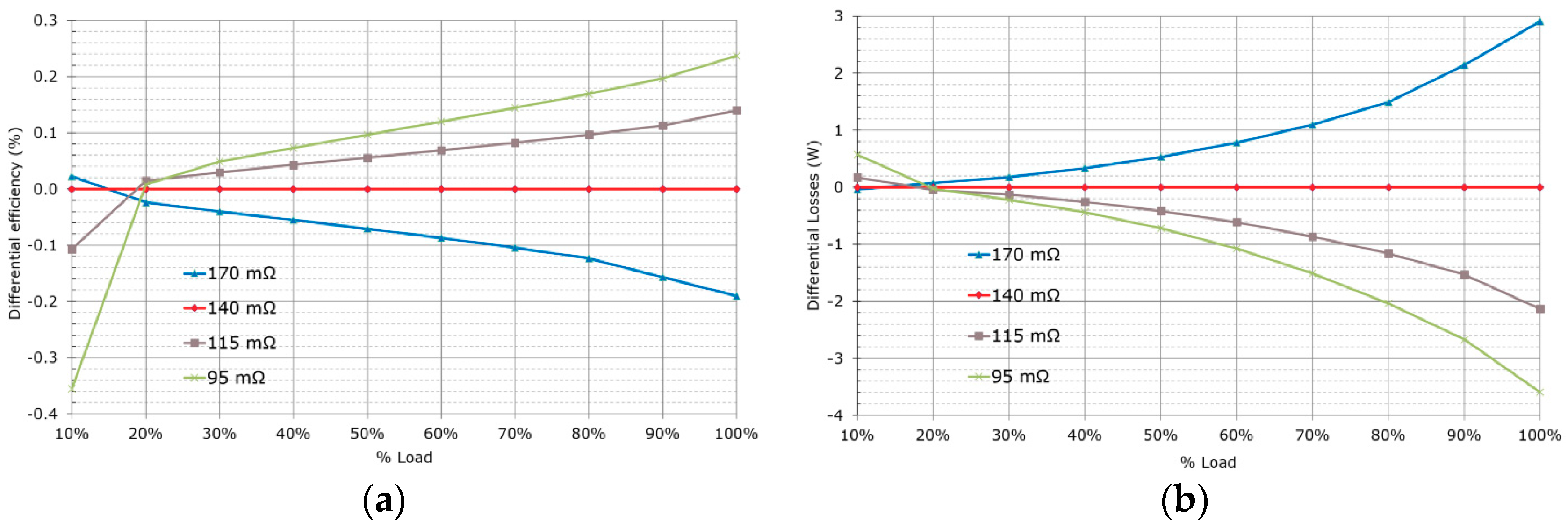
Figure 14.
Efficiency for different HV MOSFETs RDS(on): (a) differential efficiencies; (b) differential losses.
Figure 14.
Efficiency for different HV MOSFETs RDS(on): (a) differential efficiencies; (b) differential losses.
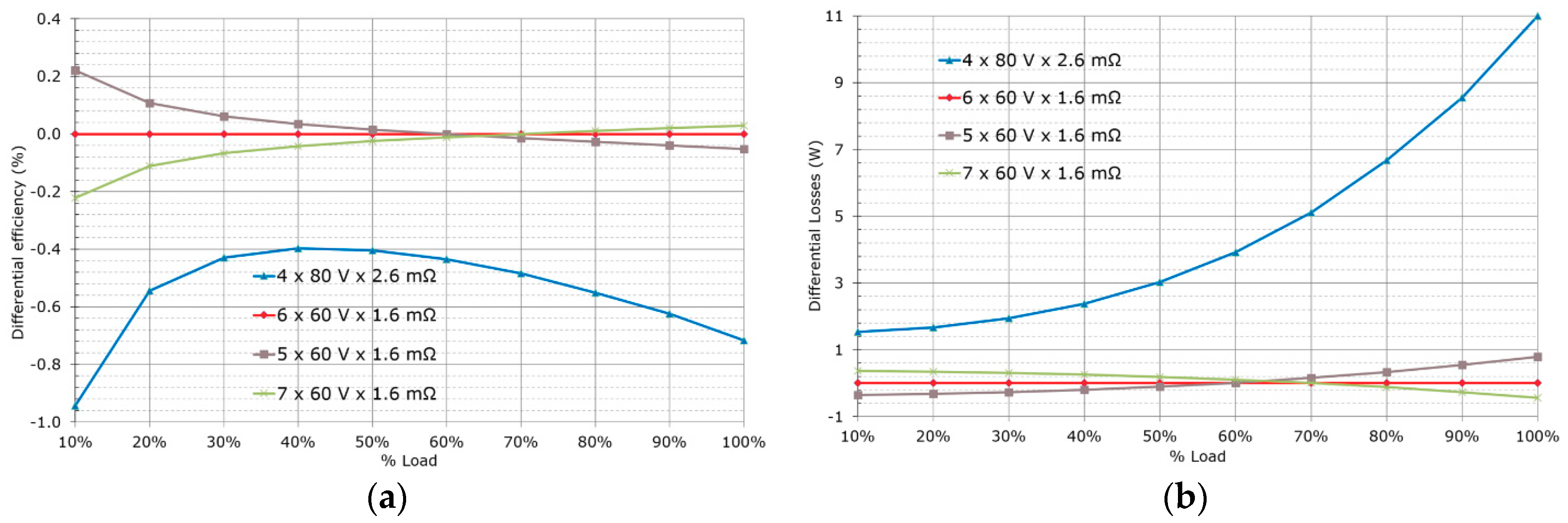
Figure 15.
Efficiency for different LV MOSFETs voltage class and number of devices: (a) differential efficiencies; (b) differential losses.
Figure 15.
Efficiency for different LV MOSFETs voltage class and number of devices: (a) differential efficiencies; (b) differential losses.
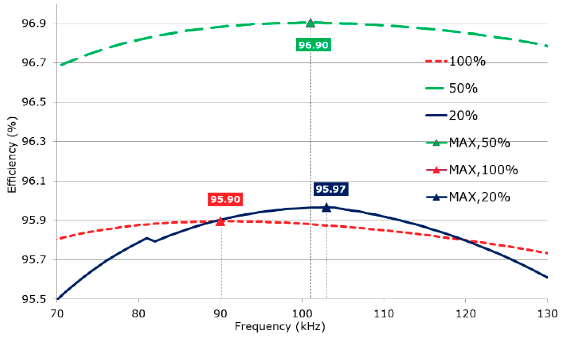
Figure 16.
Efficiency plot of the system as a function of the switching frequency. Not including fan. Keeping the wide input design maintaining a minimum freewheeling time (Lr is updated for each frequency in consequence).
Figure 16.
Efficiency plot of the system as a function of the switching frequency. Not including fan. Keeping the wide input design maintaining a minimum freewheeling time (Lr is updated for each frequency in consequence).
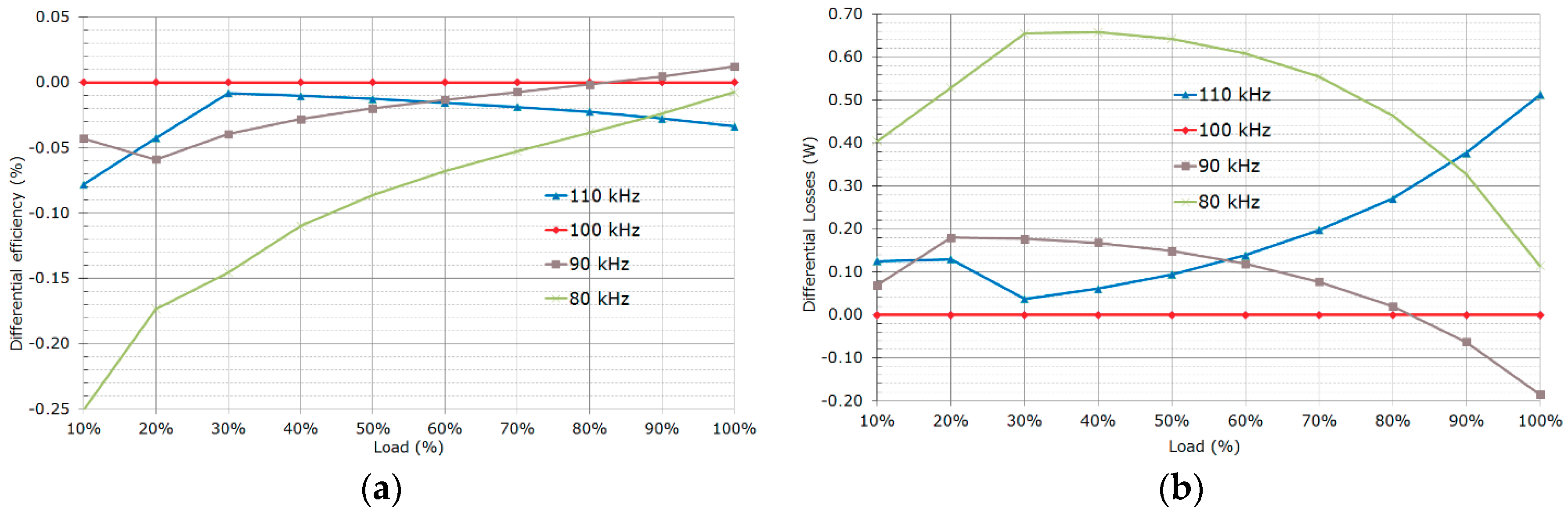
Figure 17.
Performance comparison for different switching frequencies: (a) differential efficiencies; (b) differential losses.
Figure 17.
Performance comparison for different switching frequencies: (a) differential efficiencies; (b) differential losses.
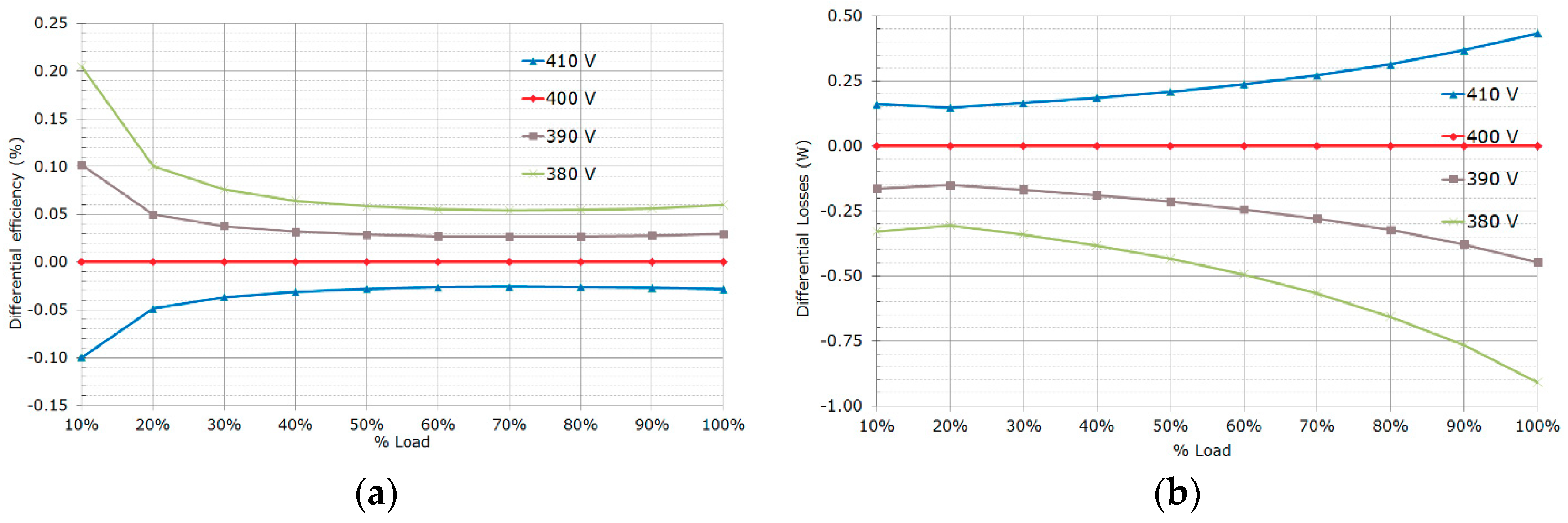
Figure 18.
Performance comparison for different nominal input voltages: (a) differential efficiency; (b) differential losses.
Figure 18.
Performance comparison for different nominal input voltages: (a) differential efficiency; (b) differential losses.
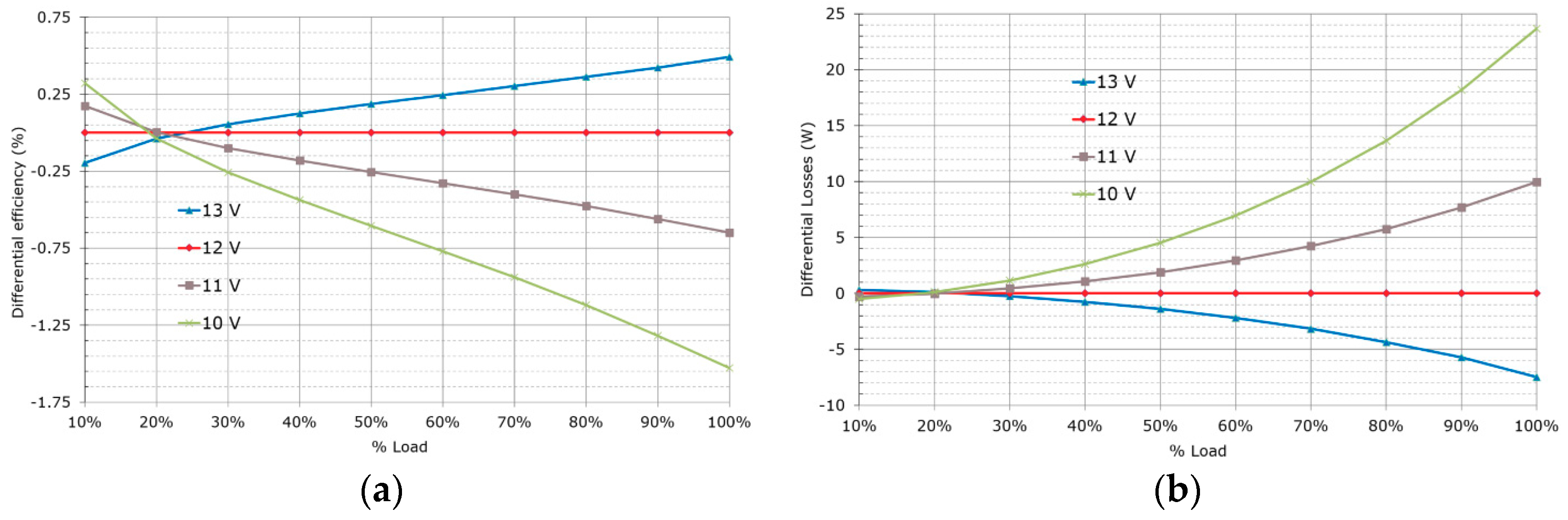
Figure 19.
Performance comparison for different nominal output voltages: (a) differential efficiency; (b) differential losses.
Figure 19.
Performance comparison for different nominal output voltages: (a) differential efficiency; (b) differential losses.
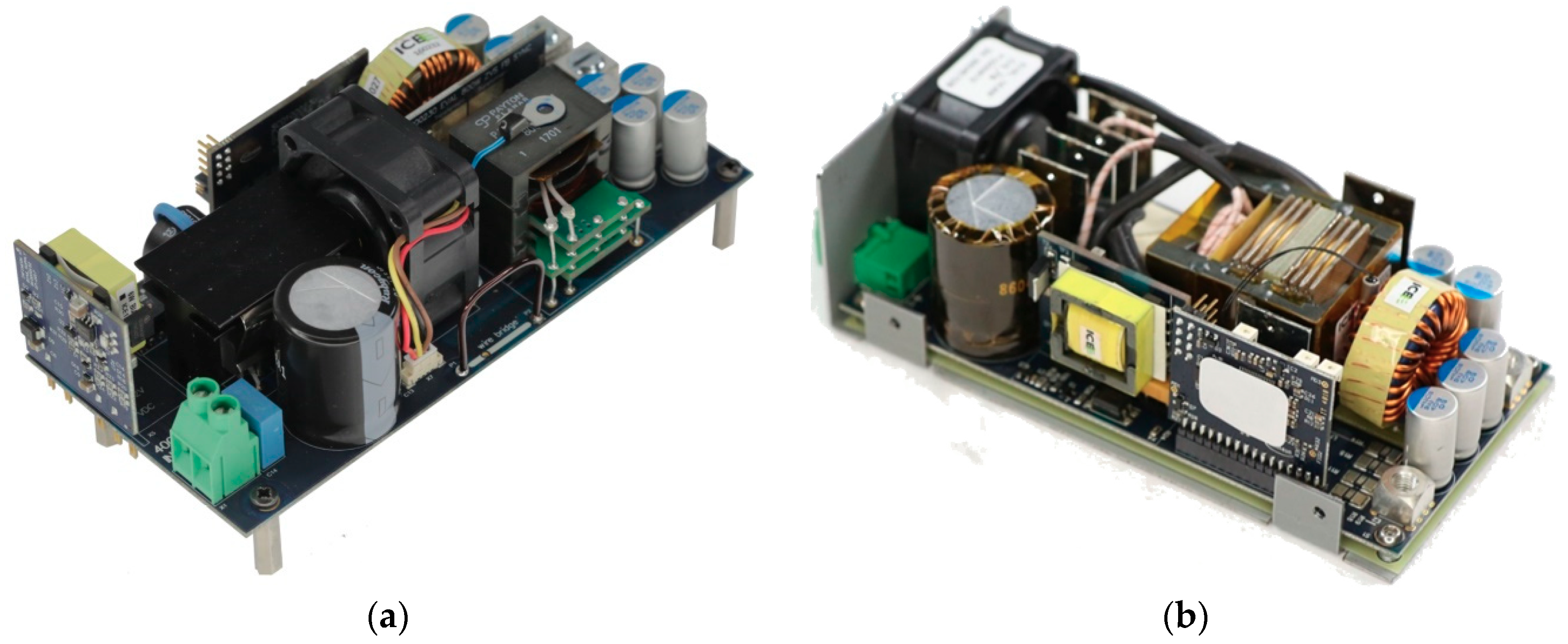
Figure 20.
Prototypes of PSFB DC-DC converter for server applications: (a) original reference design; (b) optimized design.
Figure 20.
Prototypes of PSFB DC-DC converter for server applications: (a) original reference design; (b) optimized design.
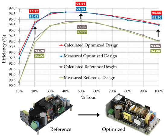
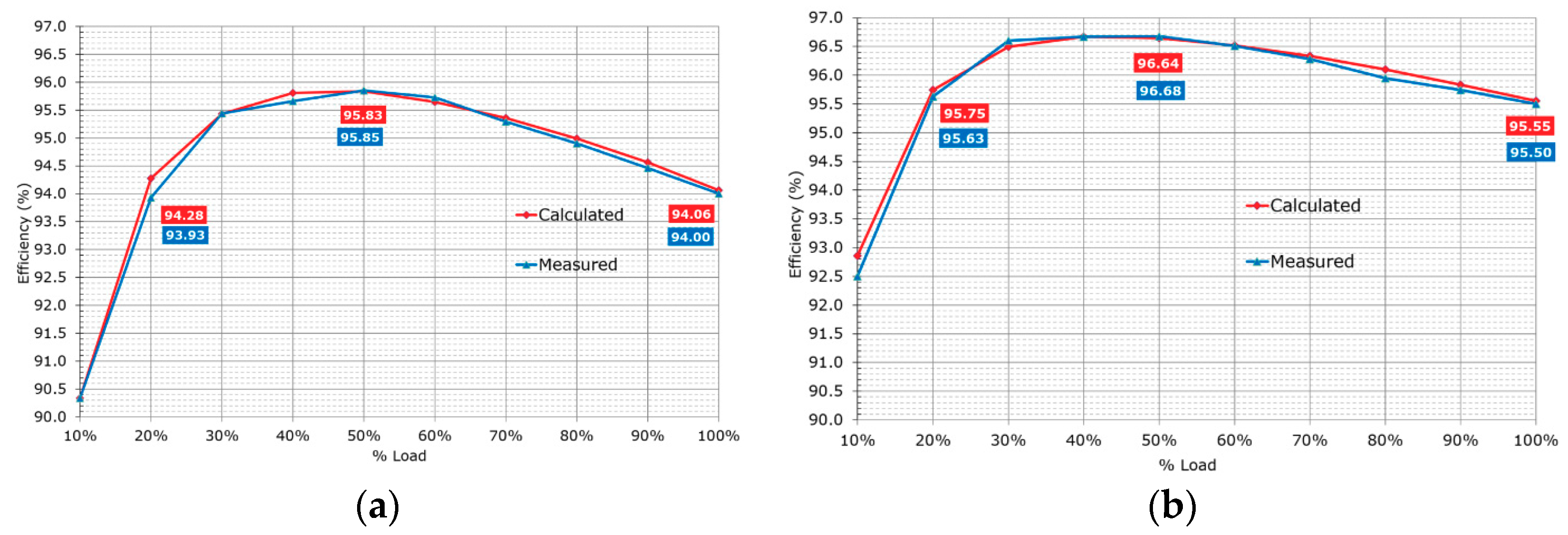
Figure 21.
Overall efficiency of the converters, including fan consumption. (a) Original reference design. (b) New optimized design.
Figure 21.
Overall efficiency of the converters, including fan consumption. (a) Original reference design. (b) New optimized design.
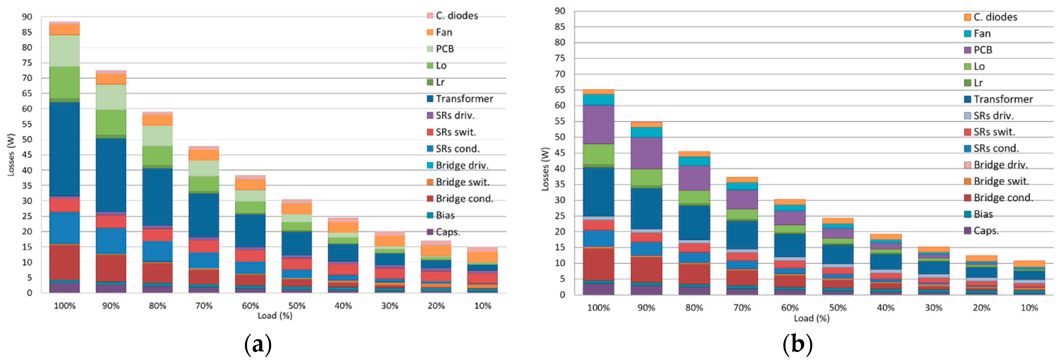
Figure 22.
Overall estimation of losses based on the loss model and the experimental results. (a) Reference design. (b) Optimized design.
Figure 22.
Overall estimation of losses based on the loss model and the experimental results. (a) Reference design. (b) Optimized design.
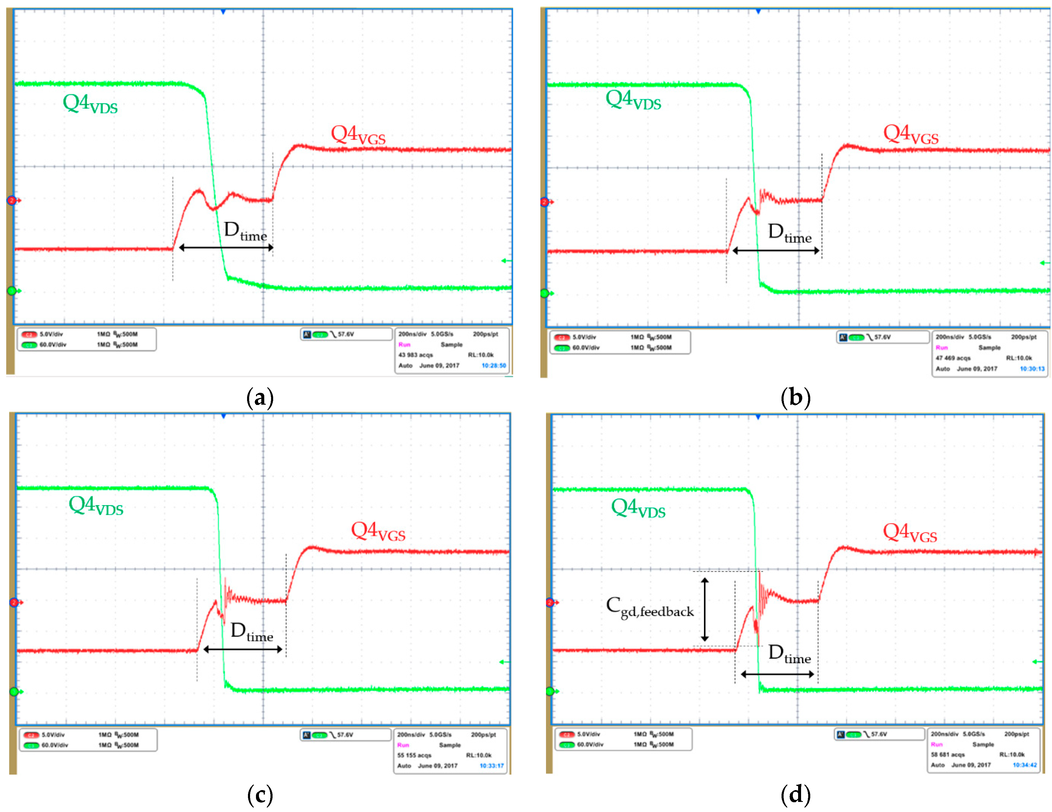
Figure 23.
Turn on switching waveforms of the low side switch of the leading leg at different loads (Io,avg). (a) 25 A; (b) 60 A; (c) 75 A; (d) 117 A.
Figure 23.
Turn on switching waveforms of the low side switch of the leading leg at different loads (Io,avg). (a) 25 A; (b) 60 A; (c) 75 A; (d) 117 A.
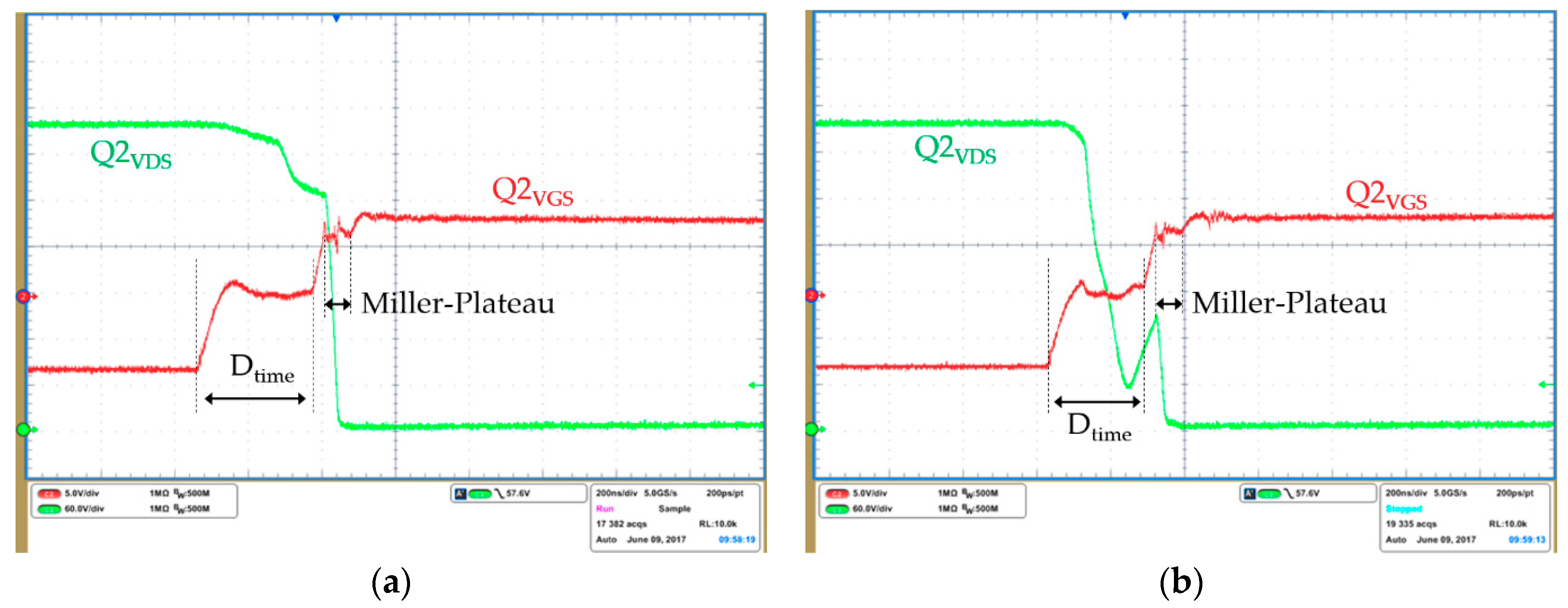
Figure 24.
Turn on switching waveforms of the low side switch of the lagging leg at different loads (Io,avg). (a) 25 A of load; (b) 60 A of load; (c) 75 A of load; (d) 117 A of load (100%).
Figure 24.
Turn on switching waveforms of the low side switch of the lagging leg at different loads (Io,avg). (a) 25 A of load; (b) 60 A of load; (c) 75 A of load; (d) 117 A of load (100%).
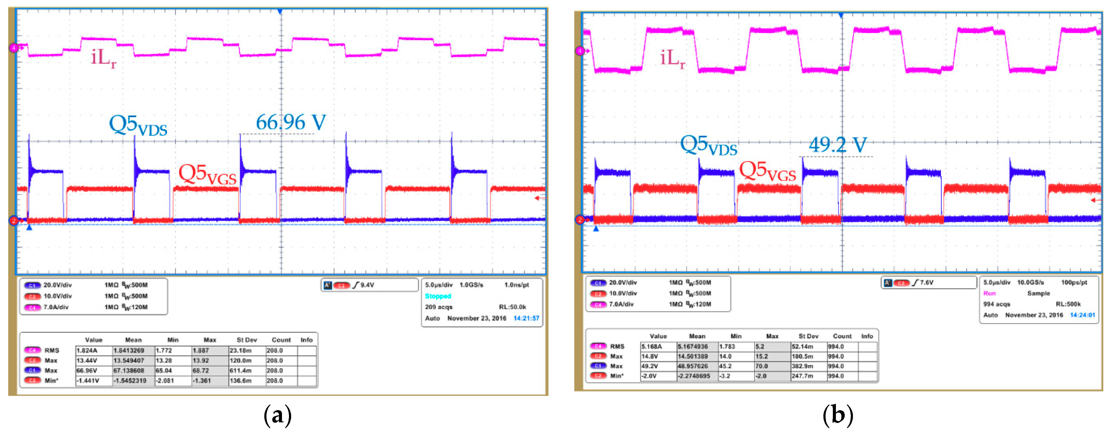
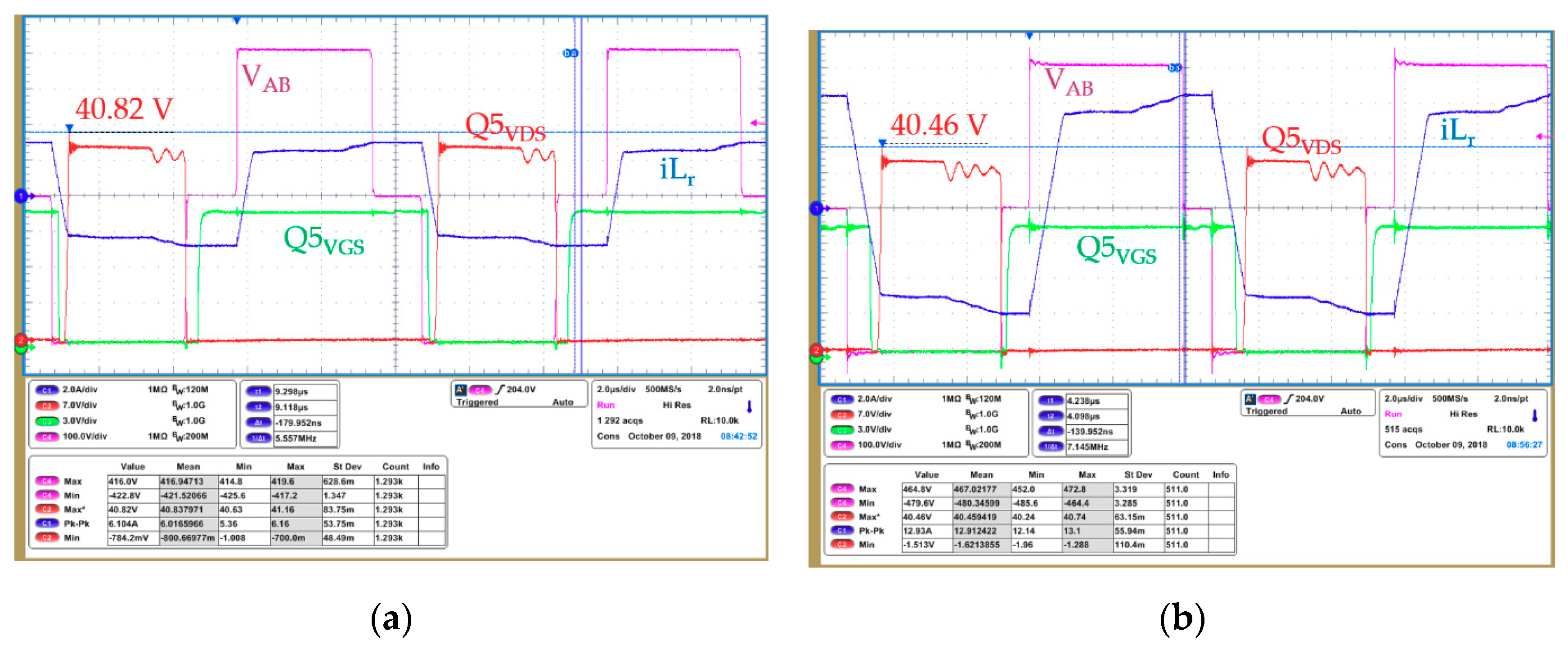
Figure 25.
SRs drain voltage overshoot: (a) Working at 140 W of output power (10% of load); (b) working at 1400 W of output power (full load).
Figure 25.
SRs drain voltage overshoot: (a) Working at 140 W of output power (10% of load); (b) working at 1400 W of output power (full load).
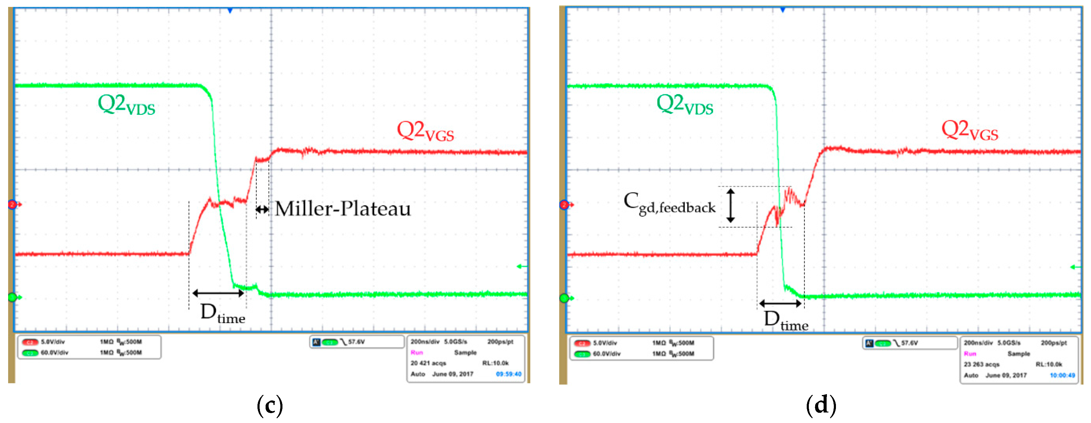
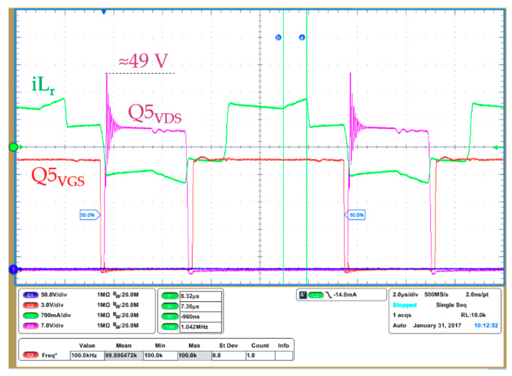
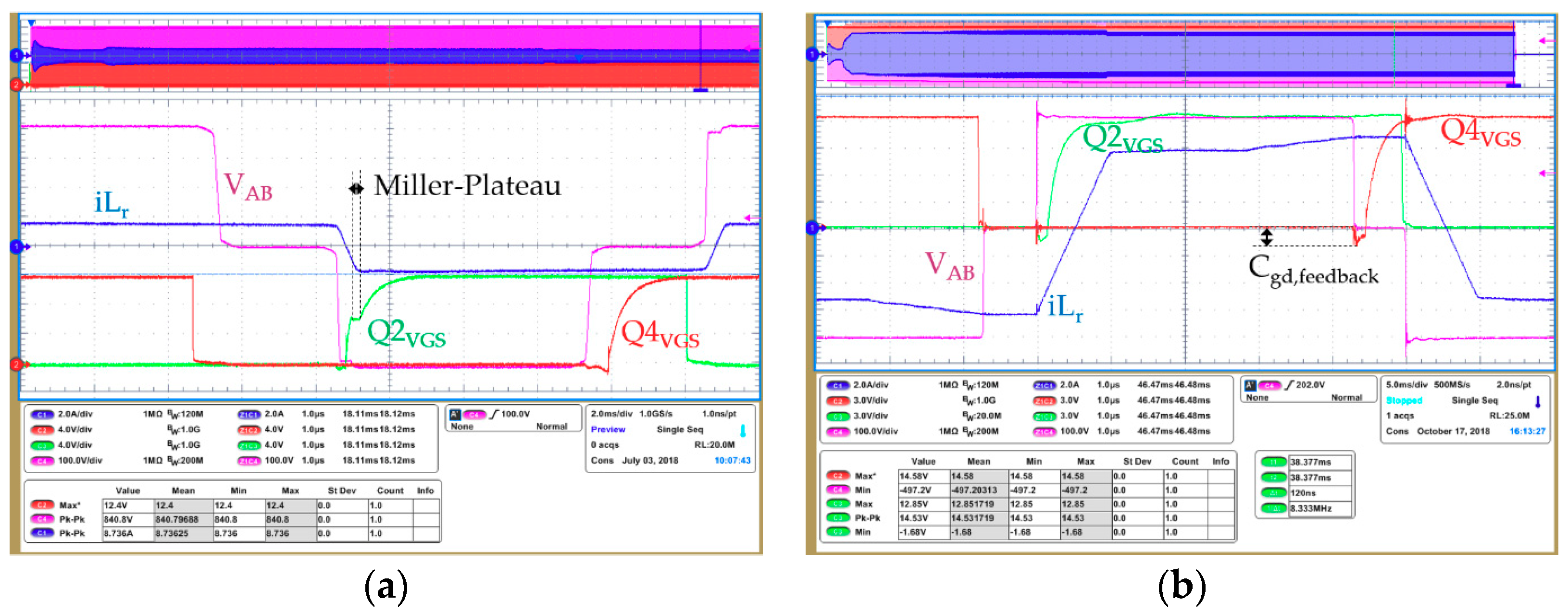
Figure 26.
Detail on the SRs overshoot and the primary side current with the clamping diodes on the leading leg position.
Figure 26.
Detail on the SRs overshoot and the primary side current with the clamping diodes on the leading leg position.
Figure 27.
Primary side HV MOSFETs ZVS: (a) ZVS at 20 A of load; (b) ZVS at full load.
Figure 27.
Primary side HV MOSFETs ZVS: (a) ZVS at 20 A of load; (b) ZVS at full load.
Figure 28.
SRs drain voltage overshoot: (a) Working at 140 W of output power (10% of load); (b) working at 1400 W of output power (full load).
Figure 28.
SRs drain voltage overshoot: (a) Working at 140 W of output power (10% of load); (b) working at 1400 W of output power (full load).
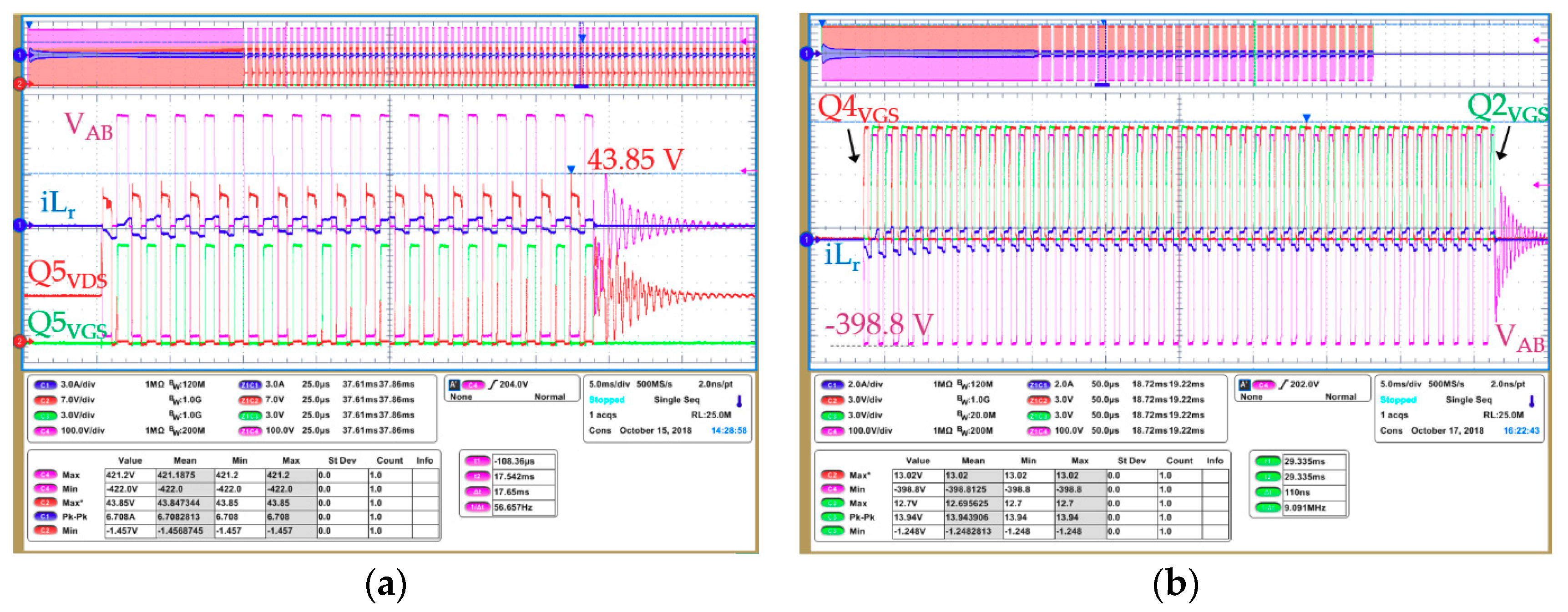
Figure 29.
SRs and HV bridge MOSFETs overshoot during burst: (a) SRs drain voltage overshoot; (b) HV bridge overshoot.
Figure 29.
SRs and HV bridge MOSFETs overshoot during burst: (a) SRs drain voltage overshoot; (b) HV bridge overshoot.
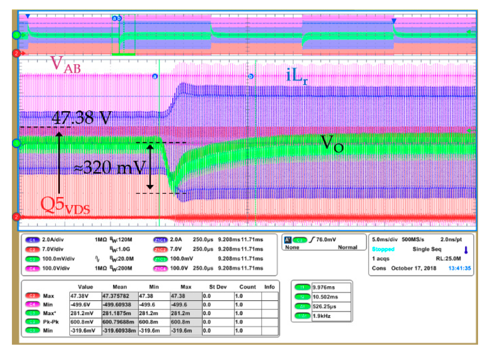
Figure 30.
SRs overshoot during load jump.
Figure 30.
SRs overshoot during load jump.
Table 1.
Summary of efficiency requirements of 80 PLUS certification for redundant power supplies.
Table 1.
Summary of efficiency requirements of 80 PLUS certification for redundant power supplies.
| 80 PLUS Certification | 230 V Internal Redundant (Complete Power Supply Unit (PSU)) |
|---|
| % of Rated Load | 10% | 20% | 50% | 100% |
|---|
| 80 PLUS Bronze | - | 81% | 85% | 81% |
| 80 PLUS Silver | - | 85% | 89% | 85% |
| 80 PLUS Gold | - | 88% | 92% | 88% |
| 80 PLUS Platinum | - | 90% | 94% | 91% |
| 80 PLUS Titanium | 90% | 94% | 96% | 91% |
Table 2.
Si LV MOSFETs.
| Parameter | BSC026N80NS5 | BSC027N60LS5 |
|---|
| VDS,max | 80 V | 60 V |
| RDS(on),max | 2.6 mΩ at 25 °C | 2.7 mΩ at 25 °C |
| Qoss | 88 nC | 43 nC |
| Qrr | 92 nC | 36 nC |
Table 3.
Summary of converter design specifications.
Table 3.
Summary of converter design specifications.
| Parameter | Minimum | Nominal | Maximum |
|---|
| Vin | 360 | 400 | 415 |
| Vout | 11.5 | 12 | 12.5 |
| Iout | 0 | - | 117 |
Table 4.
Primary side HV MOSFETs and synchronous rectifiers (SRs) MOSFETs in reference design.
Table 4.
Primary side HV MOSFETs and synchronous rectifiers (SRs) MOSFETs in reference design.
| Designator | Part Number | Units | V(BR)DSS | RDS (on) |
|---|
| Bridge (Q1–Q4) | IPP60R170CFD7 | 4 | 600 V | 170 mΩ |
| SR (Q5–Q6) | BSC026N80NS5 | 8 | 80 V | 2.6 mΩ |
Table 5.
Primary side HV MOSFETs and SRs MOSFETs in optimized design.
Table 5.
Primary side HV MOSFETs and SRs MOSFETs in optimized design.
| Designator | Part Number | Units | V(BR)DSS | RDS (on) |
|---|
| Bridge (Q1–Q4) | IPL60R140CFD7 | 4 | 600 V | 140 mΩ |
| SR (Q5–Q6) | BSC016N60NS5 | 12 | 60 V | 1.6 mΩ |
Table 6.
Inductance values and their winding realization in reference design.
Table 6.
Inductance values and their winding realization in reference design.
| Designator | Inductance | Turns | Windings | Strands | Diameter |
|---|
| Lm | 1.2 mH | 44 | 1 | 1 | 0.35 mm |
| Lr | 12 µH | 6 | 1 | 105 | 0.071 mm |
| Lo | 5.65 µH | 6 | 5 | 1 | 1.25 mm |
Table 7.
Inductance values and their winding realization in optimized design.
Table 7.
Inductance values and their winding realization in optimized design.
| Designator | Inductance | Turns | Windings | Strands | Diameter |
|---|
| Lm | 1.2 mH | 21 | 2 | 7 | 0.3 mm |
| Lr | 29.5 µH | 8 | 1 | 140 | 0.1 mm |
| Lo | 1.88 µH | 5 | 5 | 1 | 1.45 mm |
Table 8.
Magnetic core selection in reference design.
Table 8.
Magnetic core selection in reference design.
| Designator | Part Number | Manufacturer | Material | Permeability |
|---|
| Tr. Core | EQ30 | TDG | TP4A | 2400 µ |
| Lr. Core | EQ30 | TDG | TP4A | 2400 µ |
| Lo. Core | C058930A2 | Magnetics | High Flux | 125 µ |
Table 9.
Magnetic core selection in optimized design.
Table 9.
Magnetic core selection in optimized design.
| Designator | Part Number | Manufacturer | Material | Permeability |
|---|
| Tr. Core | PQ35/28 | DMEGC | DMR95 | 3300 µ |
| Lr. Core | PQI35/23 | DMEGC | DMR95 | 3300 µ |
| Lo. Core | HP 270 | Chang Sung | HP | 60 µ |
Table 10.
Summary of efficiency requirements for back-end power factor correction (PFC) AC-DC stage.
Table 10.
Summary of efficiency requirements for back-end power factor correction (PFC) AC-DC stage.
| 80 PLUS Certification | 230 V Internal Redundant (PFC AC-DC stage) |
|---|
| % of Rated Load | 10% | 20% | 50% | 100% |
|---|
| 80 PLUS Bronze | - | 84.5% | 87.7% | 84.6% |
| 80 PLUS Silver | - | 88.7% | 91.9% | 88.8% |
| 80 PLUS Gold | - | 91.8% | 95.0% | 91.9% |
| 80 PLUS Platinum | - | 93.9% | 97.0% | 95.1% |
| 80 PLUS Titanium | 96.9% | 98.1% | 99.1% | 95.1% |
Table 11.
Summary of the distribution of losses in the reference design.
Table 11.
Summary of the distribution of losses in the reference design.
| Contribution | 100% Load | 50% Load | 20% Load |
|---|
| Bias | 0.96 W | 0.96 W | 0.96 W |
| Fan | 3.45 W | 3.45 W | 3.45 W |
| Tr. Core | 0.53 W | 1.28 W | 1.59 W |
| Tr. Conduction | 29.98 W | 6.53 W | 1.07 W |
| Lr Core | 0.18 W | 0.08 W | 0.02 W |
| Lr Conduction | 1.20 W | 0.26 W | 0.04 W |
| Lo Core | 0.58 W | 0.58 W | 0.58 W |
| Lo Conduction | 9.65 W | 2.17 W | 0.33 W |
| Bridge Conduction | 11.24 W | 2.29 W | 0.33 W |
| Bridge Switching | 0.42 W | 0.42 W | 1.29 W |
| Bridge Driving | 0.18 W | 0.18 W | 0.18 W |
| SRs Conduction | 10.29 W | 2.63 W | 0.48 W |
| SRs Switching | 4.33 W | 3.70 W | 3.35 W |
| SRs Driving | 0.89 W | 0.89 W | 0.89 W |
| Clamping Diodes | 0.9 W | 1.30 W | 1.50 W |
| Capacitors | 3.28 W | 1.13 W | 0.53 W |
| PCB | 10.32 W | 2.58 W | 0.41 W |
| Total | 88.38 W | 30.43 W | 17.00 W |
Table 12.
Summary of the distribution of losses in the optimized design.
Table 12.
Summary of the distribution of losses in the optimized design.
| Contribution | 100% Load | 50% Load | 20% Load |
|---|
| Bias | 0.96 W | 0.96 W | 0.96 W |
| Fan | 3.45 W | 1.55 W | 0.60 W |
| Tr. Core | 2.37 W | 2.37 W | 2.37 W |
| Tr. Conduction | 13.04 W | 3.61 W | 0.96 W |
| Lr Core | 0.30 W | 0.15 W | 0.05 W |
| Lr Conduction | 0.64 W | 0.17 W | 0.04 W |
| Lo Core | 0.39 W | 0.39 W | 0.39 W |
| Lo Conduction | 6.18 W | 1.43 W | 0.23 W |
| Bridge Conduction | 10.05 W | 2.51 W | 0.53 W |
| Bridge Switching | 0.49 W | 0.42 W | 0.42 W |
| Bridge Driving | 0.22 W | 0.22 W | 0.22 W |
| SRs Conduction | 5.19 W | 1.28 W | 0.25 W |
| SRs Switching | 3.26 W | 2.10 W | 1.40 W |
| SRs Driving | 1.17 W | 1.17 W | 1.17 W |
| Clamping Diodes | 1.47 W | 1.67 W | 1.77 W |
| Capacitors | 3.65 W | 1.25 W | 0.58 W |
| PCB | 12.33 W | 3.09 W | 0.50 W |
| Total | 65.16 W | 24.34 W | 12.44 W |
Table 13.
Summary of difference of losses between the optimized and the reference designs.
Table 13.
Summary of difference of losses between the optimized and the reference designs.
| Contribution | 100% Load Difference | 50% Load Difference | 20% Load Difference |
|---|
| Bias | 0 W | 0 W | 0 W |
| Fan | 0 W | −1.9 W | −2.85 W |
| Tr. Core | 1.84 W | 1.09 W | 0.78 W |
| Tr. Conduction | −16.94 W | −2.92 W | −0.11 W |
| Lr Core | 0.12 W | 0.07 W | 0.03 W |
| Lr Conduction | −0.56 W | −0.09 W | 0 W |
| Lo Core | −0.19 W | −0.19 W | −0.19 W |
| Lo Conduction | −3.47 W | −0.74 W | −0.1 W |
| Bridge Conduction | −1.19 W | 0.22 W | 0.2 W |
| Bridge Switching | 0.07 W | 0 W | −0.87 W |
| Bridge Driving | 0.04 W | 0.04 W | 0.04 W |
| SRs Conduction | −5.1 W | −1.35 W | −0.23 W |
| SRs Switching | −1.07 W | −1.6 W | −1.95 W |
| SRs Driving | 0.28 W | 0.28 W | 0.28 W |
| Clamping Diodes | 0.57 W | 0.37 W | 0.27 W |
| Capacitors | 0.37 W | 0.12 W | 0.05 W |
| PCB | 2.01 W | 0.51 W | 0.09 W |
| Total | −23.22 W | −6.09 W | −4.56 W |

 ,
, 


