1. Introduction
The reliability and stability of the electrical energy generation and transportation is critical to our society. The AC grid has traditionally delivered electric power from centralized generators to end consumers, using long distance distribution lines, transformers and switches. The simplicity of these elements makes this grid very robust, but it lacks flexibility or any active control over the power flow [
1].
New trends in energy consumption and generation have transformed the grid requirements. Renewable energy sources (RES) and, consequently, energy storage systems (ESS) are being adopted as a convenient alternative to centralized generation. It is now relatively common to have distributed RES and ESS in scenarios such as telecommunications buildings, offices, data centers, universities and even in households [
2,
3]. Therefore, the distribution network has to face a wide variant system, with different actors, power flows and requirements, but it always must guarantee a stable and reliable energy flux [
4,
5].
Micro-grids or smart-grids are a popular solution to these issues [
6]. These approaches are based on splitting the grid into several autonomous sub-grids with some degree of intelligence, typically adding power converters to the traditional grid architecture. This structure can be scaled down even further to nano-grids or pico-grids and have attracted a lot of interest in recent years for applications ranging from domestic power distribution to ship and airplane electrification [
2]. Some authors also propose substituting the traditional AC distribution with DC in these sub-grids, reducing the amount of energy transformations and improving the overall efficiency. Although this is especially relevant in data centers, where it is quite common to use DC nano-grids [
7,
8,
9], it is also interesting for a household. As most of the loads in a house, RSS and ESS are DC native so it makes sense to adopt this DC nano-grid approach.
The main obstacle to the adoption of DC nano-grids at home is the lack of a suitable standard flexible enough for the user needs. As the integration of RES and ESS in a household becomes more common, the user requires outlets where active loads can either demand power or inject it back into the grid. In this paper, the design considerations of a flexible power architecture and its minimum quality of service (QoS) (i.e., voltage, stability-margins, maximum over-voltage and over-current allowed during transients, etc.) are presented for bidirectional domestic DC nano-grids.
This work is organized as follows: In
Section 2, the most suitable power architecture for bidirectional DC nano-grids is discussed. A possible implementation for these kinds of grids is presented in
Section 3.
Section 4 describes the main design aspects of a bus provider, the power converter which serves as an interface between the grid and the end-user. A design example and main experimental results for a bidirectional bus provider of ±500 W interfacing a 380 V DC bus with a 24 V DC bus is presented in
Section 5. Finally, the main conclusions reached in this work are summarized in
Section 6.
2. From AC to DC Distribution in Households
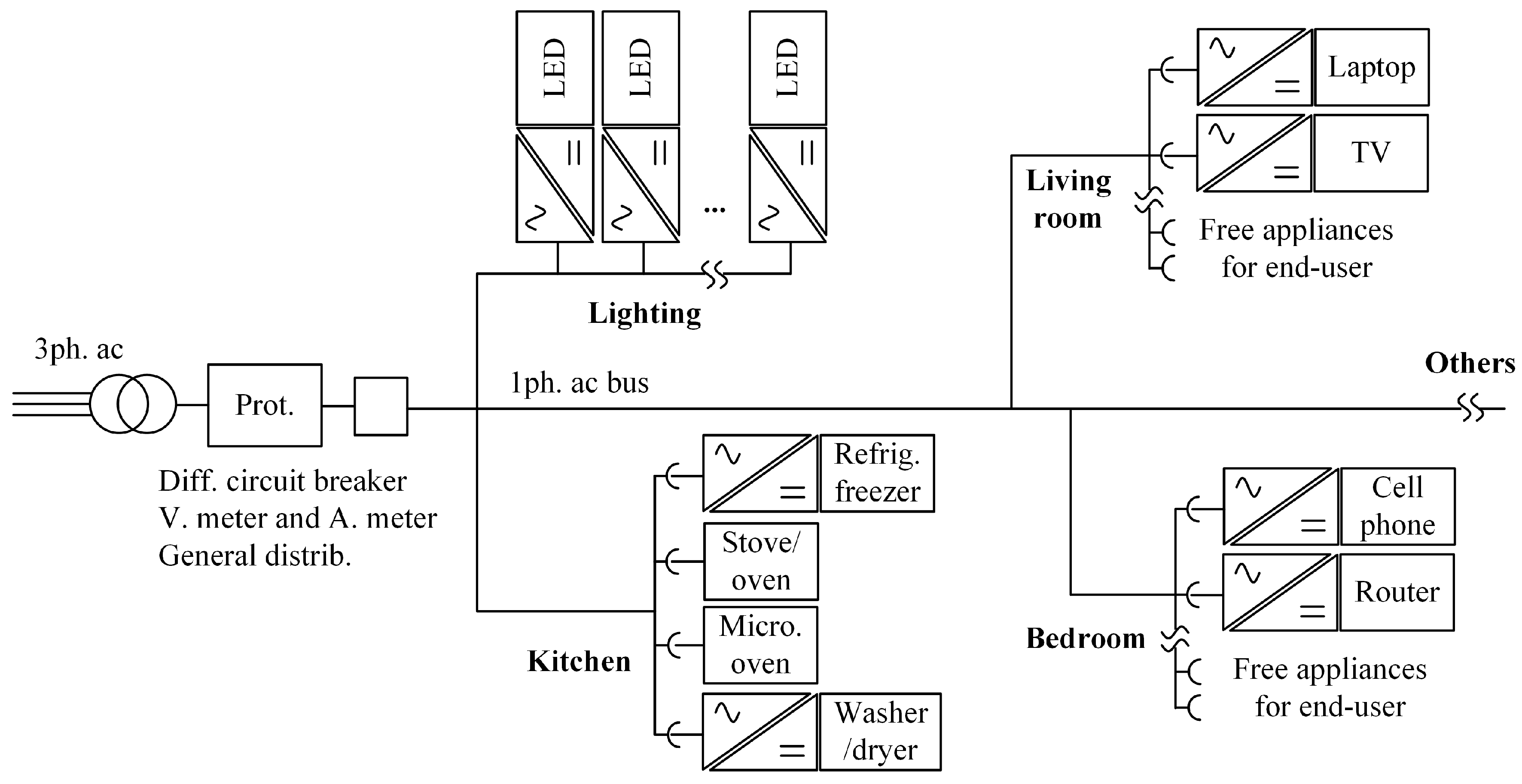
Figure 1 shows a traditional single-phase AC distribution for a household with a single connection point to the medium voltage grid. It can be seen how the system includes centralized protection and metering devices between the connection point and the distribution circuits. These circuits supply power to different areas of the home (three rooms in
Figure 1) and some specific applications such as lighting or the heater, which have been omitted in the figure.
Some key facts of this system can be highlighted. First, there is no need for bidirectional power flow in the grid. All loads are passive and they only draw power. Second, just a few loads can be directly connected to the grid without a front-end power converter. This could be the case of a traditional electric stove/oven or a light bulb. Even though these loads can work with an AC voltage, the former are not so common anymore (induction stove heaters require a power conversion) and the latter has been replaced by fluorescent lamps with electronic ballast and LED. Other domestic loads are interfaced with a power converter, typically an isolated rectifier stage. Third, these front-end converters are responsible for the power quality of the AC bus (i.e., power factor (PF) and total current harmonic distortion (THDi)) and have to comply with some regulations such as IEC 61000-3-2, Energy Star or 80 PLUS. Finally, the total power is limited at the distribution point by the protection device. This means that a single load could consume all the available power and there is no active control to share this power among different loads.
The first appearance of a bidirectional power flow in the traditional AC grid was the Uninterruptible Power Supply Systems (UPS) [
10]. These devices can provide limited energy from their batteries to the domestic nano-grid if the distribution grid fails. Although they could be used in homes, they are more common in offices and commercial buildings. Moreover, most UPSs remain fully charged and on rare occasions are charged directly through the same grid they are backing up. An example of this can be found in [
11], where the UPS compensates voltage sags within the AC facility, guaranteeing the QoS.
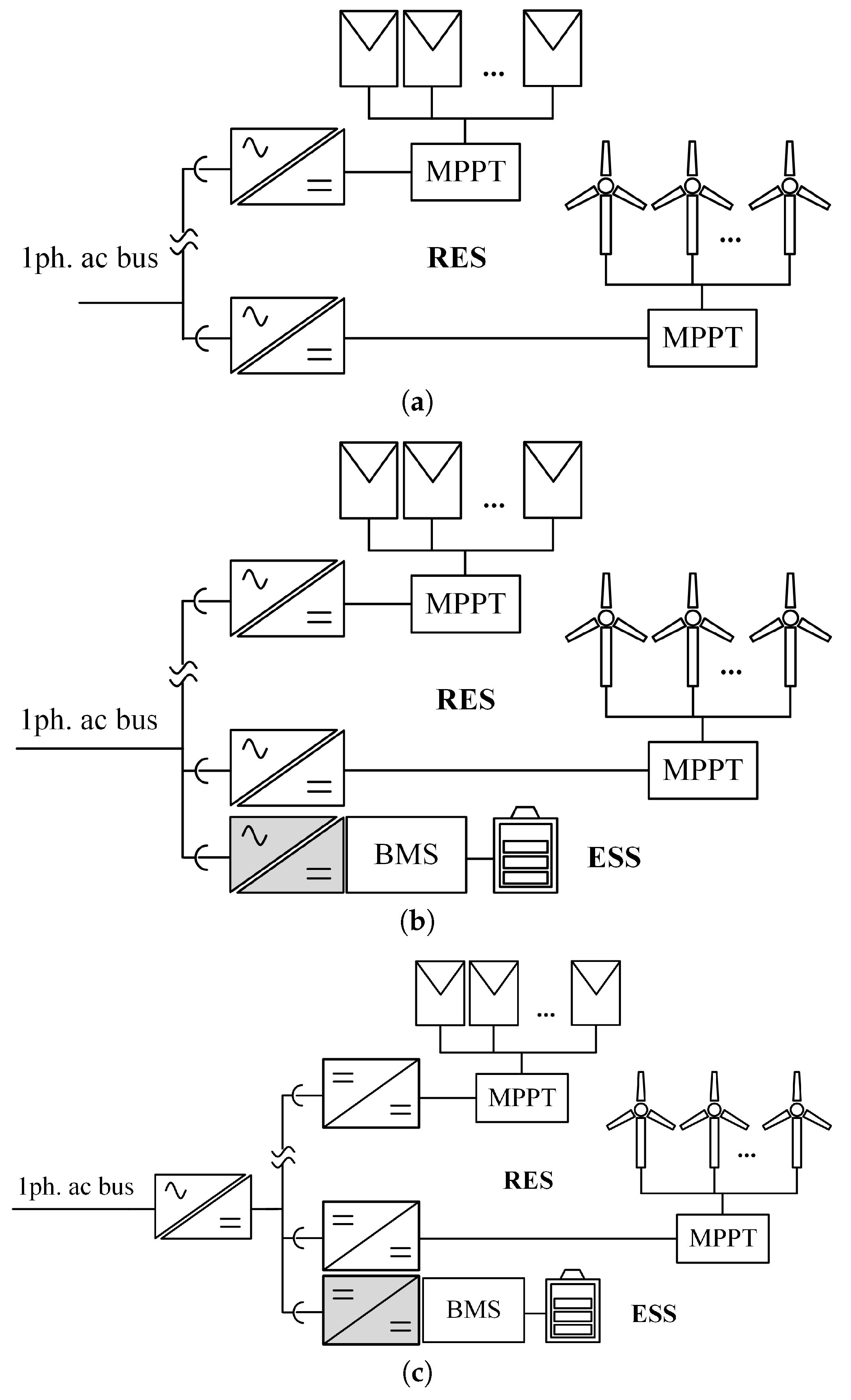
RES can help the user reduce cost and energy consumption; however, they can be troublesome. The user can connect these RES to the AC-grid in different ways, as shown in
Figure 2. One option is connecting them directly to the AC bus without any kind of ESS, as in
Figure 2a. This requires a maximum power point tracker (MPPT) DC–DC power converter and a grid-tied inverter. Although both functions could be integrated into a single converter, this adds complexity and cost to the system. Power consumption is only reduced when the RES are operating, which may not be the most convenient times.
The second option, shown in
Figure 2b, has additional flexibility. The use of ESS, typically batteries, takes full advantage of the RES coordinating energy generation and consumption. The battery management system (BMS) can monitor the net power flow in the grid and charge the energy when the power consumption is lower and discharge it to reduce the power demand at peak times. In this scheme, the ESS can be connected to any point of the grid, using a bidirectional rectifier/inverter cascaded with the BMS.
The third option is depicted in
Figure 2c. In this case, the ESS is integrated in the RES. Both RES and ESS form a DC pico-grid that uses a single inverter as interface to the AC grid. This interface can be unidirectional or bidirectional, depending on whether the ESS can be charged from the grid and the RES or only from the RES.
The preferred option among the three previous schemes is that shown in
Figure 2b. The main reason is the flexibility and reliability of this connection when compared to the scheme depicted in
Figure 2c. However, the latter could be extended, having a DC pico-grid which covers the full household. Since most of the loads, ESS and RES use DC voltage, replacing the AC distribution bus with a DC one could reduce the number of power conversions and increase the overall energy efficiency. Each element can be connected to the bus through a single DC–DC converter. Although a power conversion is still needed, the use of a DC distribution simplifies management of the grid harmonic content in the grid and helps reduce the Electromagnetic Interference (EMI) filters of each power converter.
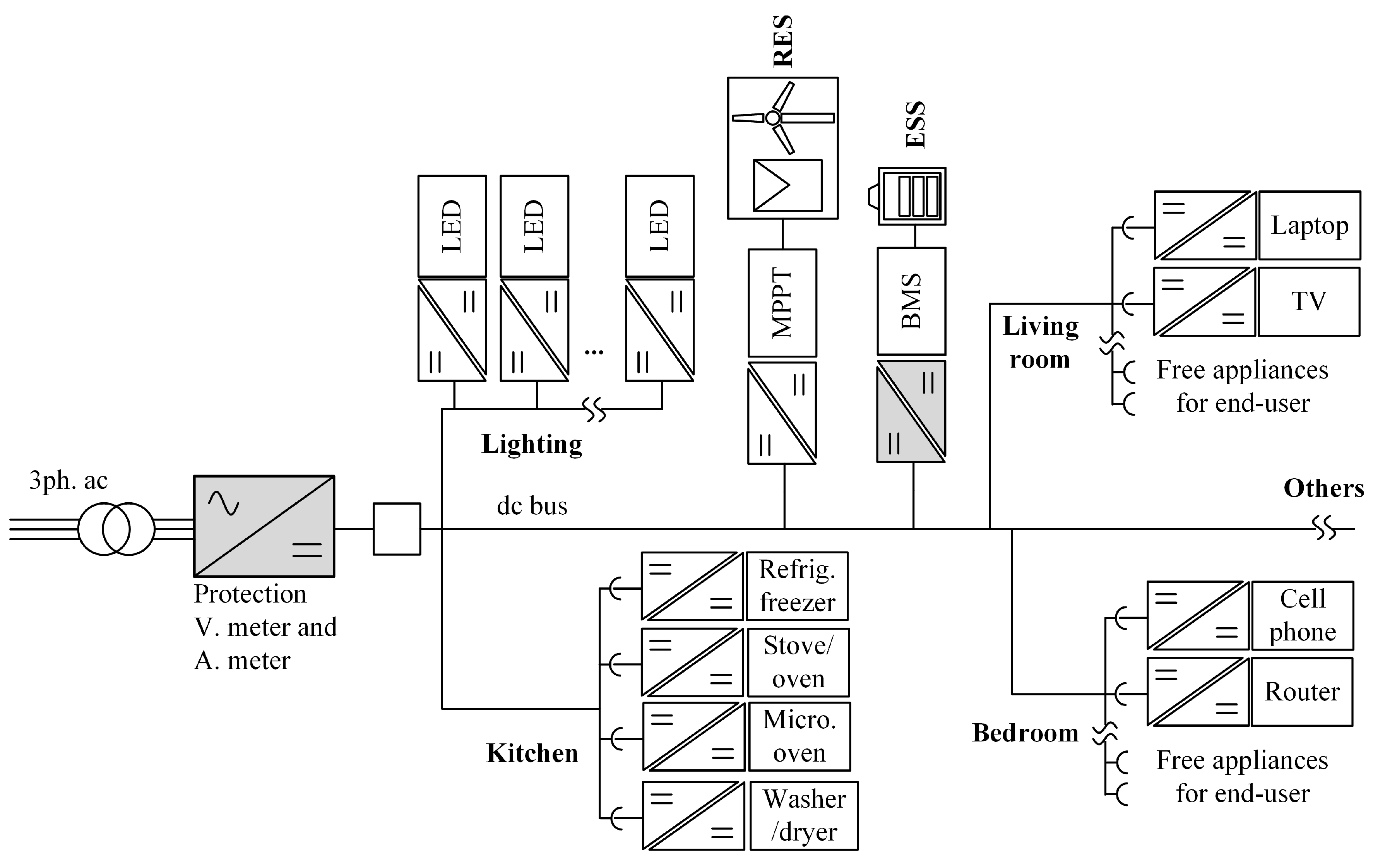
An example of a single DC bus distribution in a household is shown in
Figure 3. The integration of RES and ESS in the grid is straightforward as all the converters involved are operated in DC. Moreover, a bidirectional active rectifier provides the single access point to the mains now. Despite this active rectifier not being required, it illustrates the most flexible scenario for the DC grid, which could operate in three different modes:
Grid sourcing. This mode happens when there is power flowing from the mains to the DC grid. In other words, there is more power consumed than the one generated or stored.
Grid sinking. The DC grid enters this mode when the RES is generating more power than the one that is consumed and the ESS is fully charged. In such a case, the power can be injected back to the mains.
Islanded. If there is no power coming from the mains, the DC grid operates in islanded mode. Depending on the power demanded by the loads, the power generated by the RES and the state-of-charge of the ESS, the DC grid could remain operating in this mode for a certain period of time.
3. Proposed Architecture for Bidirectional DC Nano-Grids
3.1. Power Architecture
Voltage levels in domestic DC nano-grids are a controversial topic. Most authors have chosen 380 V as the preferred voltage for the DC bus [
3,
8,
12,
13,
14]. This voltage can provide high power levels with relatively low currents and is similar to the rms value of the 230 V ac bus. However, it is not safe against direct contacts and has other issues such as how to implement circuit breakers or in-socket arc-extinguishers.
In order to overcome these issues, two different solutions have been provided in the literature. The first one is based on a symmetrical bipolar DC bus like that in [
8]. This has the same efficiency as the unipolar 380 V buses but is slightly safer and requires a third wire. The second solution is based on two or more DC buses with different voltage levels [
4,
7,
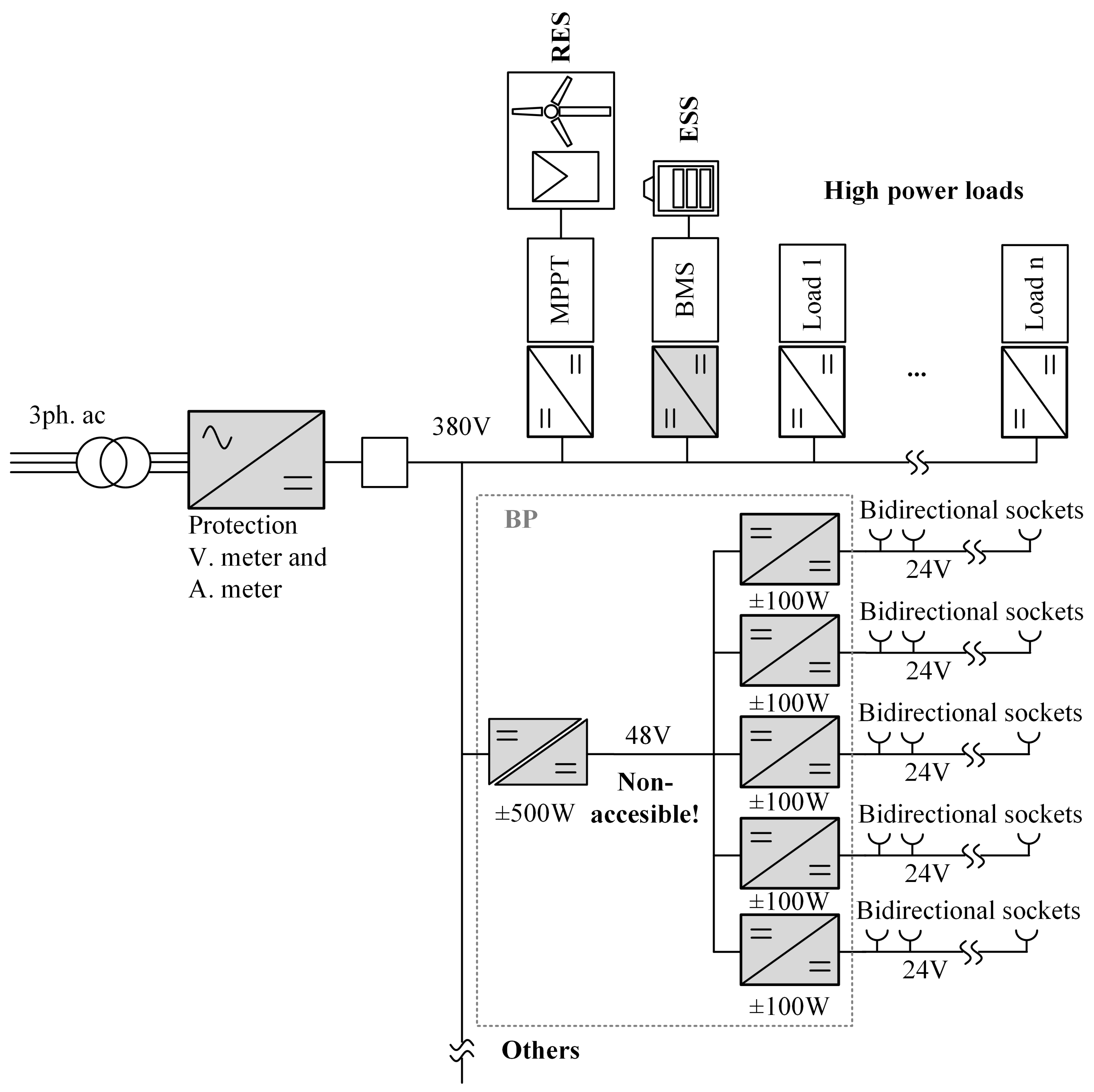
15]. The high voltage DC bus (HV bus) is used for high power loads, RES and ESS, which are rarely disconnected from the grid. The user will connect most of the portable loads to safe, fully accessible low voltage DC buses (LV bus). A single isolated power converter, known as the bus provider (BP), interconnects the LV and HV buses. An example of this power architecture based on two DC buses is depicted in
Figure 4.
It is not easy to set a single safe voltage for the LV bus. The most common proposals are 48 V [
4,
16], 24 V [
7,
15,
16], and 12 V [
16]. Another option is having a smart BP that is able to detect the load and to adapt its output voltage accordingly. However, this concept is way more complex than having a single bus voltage and requires a standard to specify the loads’ behaviour (e.g., USB Power Delivery standard [
17]).
Another challenge of this architecture is determining which loads can be connected to each bus.
Table 1 shows some common domestic loads, arranged by its power demand [
18,
19]. There is a clear division between loads requiring well below 100 W and those with higher demands. Hence, it seems reasonable to propose the use of the LV bus for loads that consume less than 100 W (first column) whilst the typically static appliances consuming well over 100 W should be connected to the HV bus. The third column of
Table 1 shows elements that are difficult to classify. These are portable loads that the user could plug and unplug somehow frequently, but their power consumption is clearly over the 100 W limit. A possible solution would be to connect them permanently to the HV bus. This might make sense for certain loads, such as the beater or the toaster, which are mainly located in the kitchen, and they can be seen as another white good. However, this is not true for other loads such as the drill or the vacuum cleaner, which must be, by definition, portable. The growing trend of making these tools battery operated helps mitigate this issue. The battery charger requires a rather low power and can be safely connected to the low voltage bus.
3.2. Implications of Active Loads and Bidirectional Power Flow
None of the works discussed on this paper deal with the possibility of the bidirectional power flow in the LV bus sockets. Either bidirectional converters such as the BMS or the front-end rectifier are connected to the HV bus, as shown in
Figure 4, or complex controls are applied to power sources on the LV bus. It is thus important to analyze the requirements and implications connecting active loads to the LV bus. In this work, the architecture shown in
Figure 5 is adopted for the analysis, due to the advantages previously discussed.
The key features of the proposed architecture can be summarized as follows:
The HV bus voltage is set to 380 V, according to most proposals, due to its advantages.
The LV bus voltage is set to 24 V, as a trade-off between efficiency and safety.
The BP is a bidirectional isolated power converter (see
Figure 4 again). In this specific approach, a two-stage multi-output power converter is proposed without losing generality. The first power converter provides a 48 V internal DC bus, which is safe to contact but not accessible, isolated from the 380 V. The second stage comprises several DC–DC non-isolated power converters. For simplicity, in this work, only five outputs (or channels) have been considered. Each channel should provide a 24 V bus able to source or sink power.
The maximum power of each channel of the 24 V bus is limited to ±100 W, following the conclusions of the previous section.
The maximum power of a BP is limited up to ±500 W in this example. However, it is important to note that the number of channels could be increased as well as the power of the BP overall.
There might be as many BPs as rooms or spaces the household has.
The BP can inject current into the 380 V bus but cannot regulate its voltage.
The bidirectional LV sockets are fully accessible to the user, who can connect passive and active loads. The passive loads might be small electronic loads with different power, such as those outlined in
Table 1, which can be modeled as a constant power load plus a capacitor in parallel [
4]. The interaction between the output impedance of each channel of the BP and the input impedance of these loads should be taken into account to avoid instabilities [
20,
21]. This will impose certain limitations to the loads that a user can connect to the 24 V bus.
Modeling of active loads is much more complex, as they can have many structures with very different behaviors. Most active loads will be connected to the LV bus through a power converter. If it tries to regulate its output voltage, i.e., the 24 V bus, two different converters would try to regulate the same voltage. The most common solution to this problem is droop control [
22,
23,
24,
25,
26]. However, this option has two important issues:
Due to a great variety of loads, implementing droop control in each one is quite complex. Moreover, this would require a communication protocol connecting all the elements.
Most active loads connected to the LV bus will have a limited power capability. For this reason, it does not seem convenient to rely on a current sharing technique when most of the power will be provided by the BP in all cases.
It seems reasonable to discard the use of droop control and simply configure the active loads as current sources or sinks that do not regulate the LV bus voltage. In the case of an RES, such as mini-wind turbines or small PV panels, the MPPT should simply deliver the maximum power from the generator and act as an auxiliary energy source. When it comes to ESS, the batteries connected to the 24 V bus will only store small amounts of energy. Therefore, they should be used only for reducing the power demand and not as the main energy storage system. Those RES and ESS with high power or energy capabilities should be connected to the HV bus.
3.3. QoS Definition
There are several standards that deal with QoS in military and telecommunication applications, imposing stringent restrictions on parameters such as maximum voltage ripple, the dynamics overshoot and undershoot voltages, the settling time under load variations and the load steps allowed in the bus [
27,
28]. However, there is no clear standard that defines QoS for domestic power distribution. In this work, the USB Power Delivery standard recommendations have been adapted for the QoS of 24 V bus [
29]:
The bus voltage should be kept within a ±5% of the nominal voltage.
The maximum allowed power variation is limited to 100 W.
The voltage ripple in steady state should be lower than ±0.5%.
While 200 W load steps are, in theory, possible, it is highly unlikely that a user can connect or disconnect a passive element at the exact same time they connect or disconnect an active element. Even if that was possible, the dynamics of their front-end converters are not instantaneous and would dampen the transition. For this reason, a maximum 100 W power variation is used in this work, allowing load transients from active to passive and vice versa (e.g., from 30 W to −70 W), or a no load to full load steps in the worst case (from 0 W to 100 W for passive loads, from 0 W to −100 W for active ones).
4. Bus Provider Design Considerations
The QoS previously defined fixes some design constraints in the BP. Not only the standard, but also the bidirectional power flow and the active loads impose some restrictions to the power converter design. In this section, a basic guideline is presented in order to help the designer to get a reliable and effective BP.
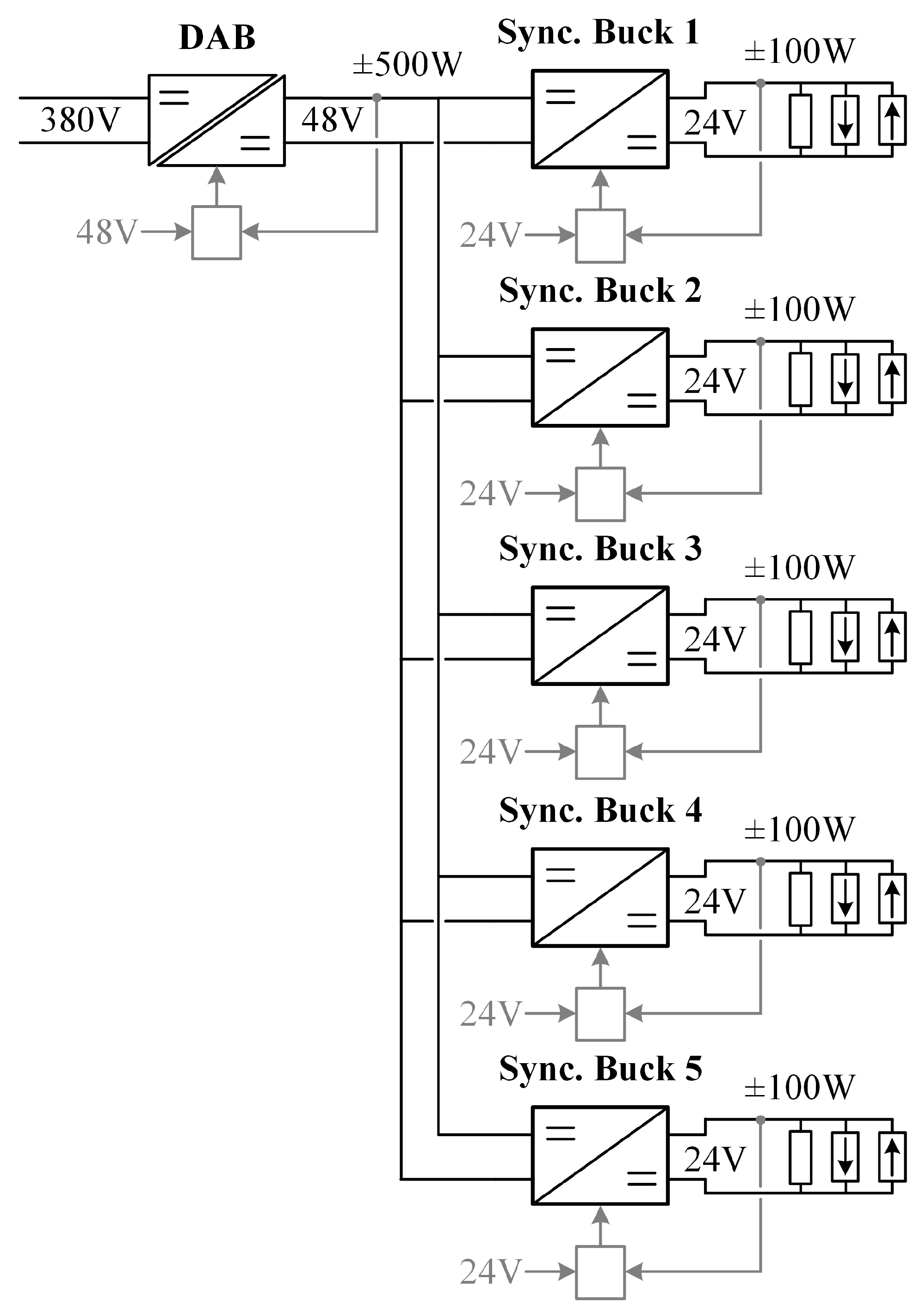
First of all, in this work, a two-stage, single-input, multiple-output bidirectional power converter has been chosen as BP. This approach has the main advantage of dividing the tasks of the power conversion: the first stage is in charge of providing the galvanic isolation, whilst the second stages are optimized for fulfilling the QoS parameters. In this particular case, the first isolated stage is a Dual Active Bridge (DAB), whilst a synchronous buck converter is chosen as second stage. A basic block diagram of the detailed power architecture of the proposed BP can be seen in
Figure 6.
The DAB is being chosen due to its symmetry, the natural bidirectional power flow control and a high efficiency due to the Zero Voltage Switching (ZVS) [
30,
31]. The synchronous buck converter is the simplest non-isolated bidirectional topology for stepping down the voltage. In addition, this topology has been widely studied and different controllers and improvements can be easily added.
4.1. Operational Modes
The presence of both active and passive loads in the 24 V bus imposes three different operational modes to the synchronous buck converter. It is worth mentioning that, in any of them, the buck converter must regulate the output voltage, independently of the power flow direction. These operational modes are the following ones:
Source mode, > 0 W. In this mode, the buck converter is providing power to the 24 V bus.
Sink mode, < 0 W. In this mode, the buck converter is sinking current from the 24 V bus to the HV bus.
No load or nearly no load, 0 W. In this mode, no net power is being transferred to any bus.
The no load scenario could be possible either if no load is connected or active and passive loads are plugged with the same amount of power (i.e., the generated power equals the demanded power). The former case is very likely and it corresponds to a free socket. Conversely, the latter is not very common and it only would happen under certain conditions.
These three operational modes are also valid for the DAB. The source mode is defined in this case as
where
is the number of buck converters used (five in this example) and
is the maximum power of the DAB (500 W for this example). In a similar way, the sink mode can be defined as
Finally, the no load or nearly no load mode is defined as
It should be noted that
can be either positive or negative; hence, the no load mode defined by Equation (
3) is more likely when compared to the buck case. This is due to the possibility of equal generation and demand of power by each single channel (i.e., by each buck converter). Multiple scenarios can fulfill this condition and they only depend on the 24 V bus load connection (i.e., it only depends on the end user). As in the case of the buck converter, the DAB must regulate its output voltage (internal 48 V) independently of the operational mode.
4.2. Synchronous Buck Converter Design Tips
As mentioned before, the synchronous buck converter is a very well-known topology and there are different controls and strategies to operate this power converter. In order to fulfill the QoS, the buck has to deal with a huge variety of potential loads and with a source/sink operation. The simplest approach is being followed here: Continuous Conduction Mode (CCM) and voltage mode regulation. However, some particular considerations have to be taken into account when designing this power stage.
4.2.1. Load Characterization and Design Approach
All the loads potentially to be connected to the 24 V bus should have a PoL converter for adapting the bus voltage to their specifications. The input impedance of this PoL can be approximated as a simple RC network, mathematically:
where
corresponds to the input equivalent capacitor and
represents the input resistance. The latter can be either positive (sink mode, the PoL behaves like a constant power source) or negative (source mode, the PoL behaves like a constant power load). The former case is not critical from dynamic behavior of the 24 V bus; the latter may introduce a Right Half Plane Zero (RHPZ) which can degrade the voltage regulation. The approximation of Equation (
4) neglects this RHPZ and it is only valid if the pole of
is below the pole introduced by the buck converter. In order to satisfy this, the only way to decrease the frequency of the pole of
is by increasing the value of
. This introduces another restriction to the output capacitor design of the buck converter. Finally, it is worth mentioning that Equation (
4) is valid for all the conduction modes and all the control modes to be applied to the buck converter.
This approximation allows for modeling the equivalent impedance of the bus in a very simple way, such as
where
M is the number of loads connected to the 24 V bus and
and
are the parallel equivalents of
and
of each PoL. Hence, once the equivalent impedance of the bus is known, a possible algorithm of design can be followed, like that proposed in [
32].
4.2.2. Implications of the Different Controls in the Design
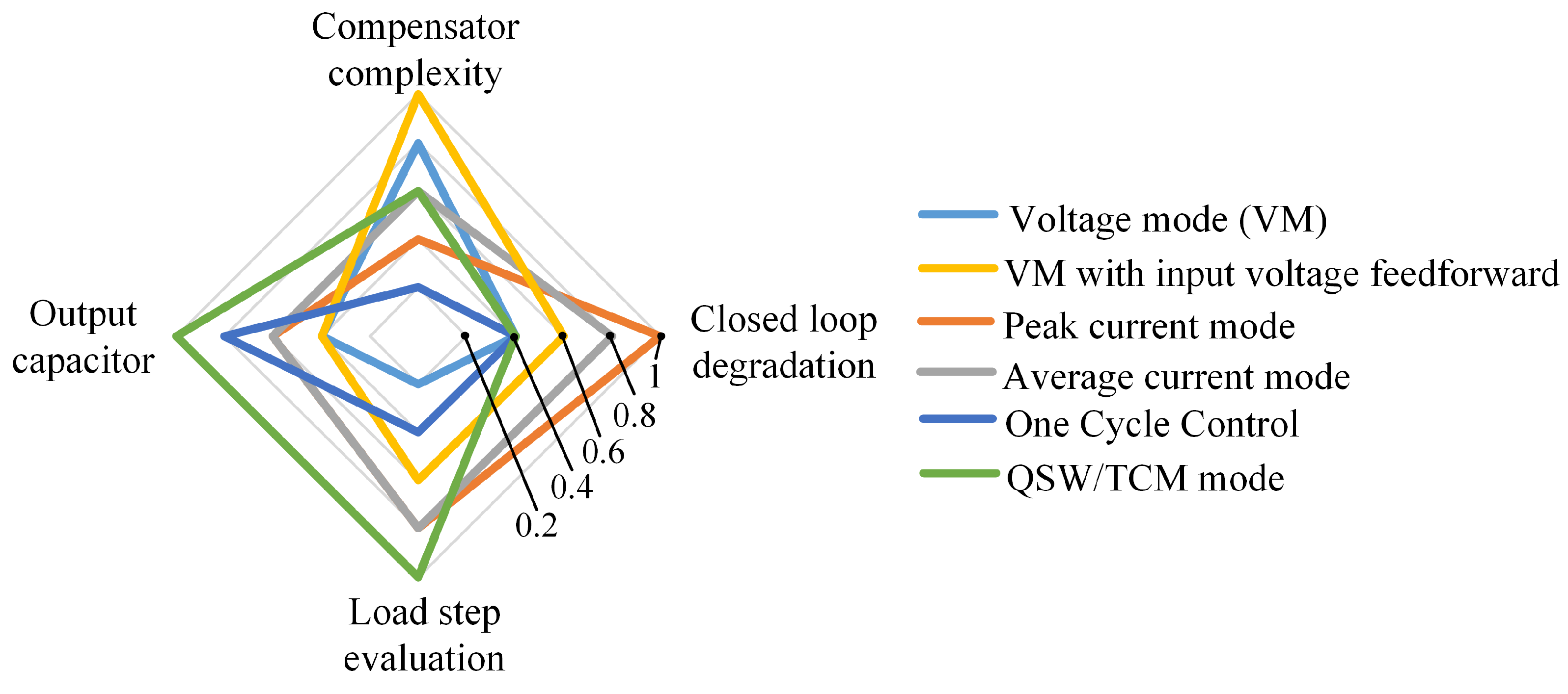
In the previous section, it was assumed that a voltage mode controller was used for the buck converter. Nevertheless, this is not the only way to regulate the output voltage. The controller stage also plays an important role when designing this power stage. This is especially relevant when the converter has to fulfill all the requirements described in the QoS and on the standards. A discussion about the possible advantages and disadvantages of the control stage is developed in this section. A quantitative analysis is used here to determine the benefits and bottlenecks of each control strategy. This analysis must take into account the following parameters:
Compensator realization. Among other advantages, the simplification of the compensator realization is probably one of the most important reasons to justify the change of the controller. A reduced order or a higher gain margin or phase margin with the same complexity should be taken into account when evaluating the controller stage. In this sense, the component count of the compensator (analog control) or the computational cost (digital controllers) can be used as metrics for comparing the controllers.
Closed loop degradation. As it was mentioned in previous sections, the degradation of the closed loop transfer function when a load is connected in the 24 V bus is critical. Some controllers may have less degradation than others may, in terms of stability margin or bandwidth. These parameters are useful to compare any controller stage.
Load step comparison. Even though it was possible to conduct a design with a controller different from voltage mode, the cost to be paid might be the reduction of the bandwidth and, as a consequence, a worse QoS from the dynamic point of view. Therefore, it is mandatory to compare the controllers in terms of dynamic response against a load step. The settling time and overshoot/undershoot voltage can be used as metrics for this purpose.
Fixed switching frequency versus variable switching frequency. Some controllers implement a variable switching frequency in order to improve the efficiency of the power converter or to simplify the dynamic behavior of it. It is not easy to compare these controllers to those that use a constant switching frequency. The typical parameter used in AC–DC power converters is the EMI filter and the harmonics of the input current (THDi). The variable switching frequency controllers usually have an increased THDi when compared to fixed switching frequency controllers and they require more complex EMI filters. However, this parameter is not very useful for a DC–DC power converter due to the lack of any regulation in terms of harmonic content. For this reason, the size of reactive components are proposed here as a possible fair metric to do this comparison. It is well known that, due to the switching frequency variation, inductance and output capacitor values may differ from those of a constant switching frequency control. In general, variable switching frequency controllers require larger inductance or capacitor values when they have to accomplish the QoS requirements. Therefore, these larger values could affect other features of the power converter.
Five additional control techniques, besides traditional voltage mode control, have been compared using the aforementioned parameters. Each parameter has been normalized to the worst case, 1 being the highest (i.e., the worst performance). The results of this comparison can be seen in
Figure 7.
The following conclusions can be summarized from this comparison:
Voltage mode with input voltage feedforward. This technique was originally proposed in [
33] as a possible way to minimize the impact of the load and input voltage variation. However, this control is based on the ideal relationship between input and output voltages. Due to this and the parasitic of the components, it makes the compensator design more difficult.
Peak current mode. This mode has the main advantage of simplifying the compensator design [
34]. Under this particular control mode, the power stage can be modeled as a second order system, but the double pole of the output filter is eliminated. Other potential advantages of this mode are the protection to short-circuit and the ability to work with large capacitive loads. However, the transfer function degradation forces using a bigger capacitor than one used in the voltage mode control.
Average current mode. An alternative to the previous controller is the average current mode [
35]. This controller avoids the need of a compensation ramp when compared to the previous one. However, this is the only significant advantage over the peak current mode. The rest of the parameters evaluated in this comparison remain very similar to those of the peak current mode.
One Cycle Control. This control technique has been proposed as an alternative to the input voltage feedforward control [
36,
37]. The main advantage of this controller is the capacity of reacting in a single switching cycle to the output voltage perturbations. In spite of its simplicity and the potential advantage from the dynamic point of view, for DC distribution, the load step is mainly limited by the output filter and not by the bandwidth of the controller. Therefore, the main advantage of this control mode is useless in this application.
Quasi-Square Wave Zero Votage Switching mode (QSW-ZVS) or Triangular Current Mode (TCM). Finally, a variable switching control has been added in the comparison. QSW-ZVS [
38] also known as TCM [
39] allows for reducing the switching losses taking advantage of a large current ripple through the inductance. Even though from the compensator complexity point of view and the closed loop degradation this mode does not have any significant disadvantage over voltage mode, it requires a much larger output capacitance. This causes the performance against load steps to be poorer when compared to the other control modes.
As can be seen, there is not any controller that has a clear advantage over the others. Nevertheless, taking into consideration all the parameters evaluated in this comparison, the voltage mode seems to be the most convenient solution for the proposed QoS. A similar analysis can be applied to any kind of topology and any potential controllers, in order to clarify which control is more appropriate to meet the requirements of the proposed standard.
4.3. DAB Design Tips
The DAB design is constrained by two conditions: the no load operation and the stability of the internal 48 V bus.
The first condition is very important for this particular topology. As in the case of the buck converter, depending on the loads connected by the end user, the DAB must regulate the 48 V bus even when no power is transferred in either direction. The DAB is a power converter that naturally works with ZVS transitions during the turn-on, allowing a reduction of the power losses. However, at light operation, this ZVS can be lost, causing the increasing of the losses and also the breakdown of the converter [
40,
41]. Several control techniques have been proposed in the literature in order to overcome this problem [
30,
42,
43,
44,
45,
46]. The majority of them deal with a wide voltage range variation (either input, output or both). However, this is not the particular case of the BP, in which both bus voltages are considered stable (the 380 V bus is regulated by other power converter, whereas the 48 V bus is regulated by the DAB). Taking into account this fact, a possible solution can be found in [
30,
43], where the use of the magnetizing inductance is proposed for extending the range of ZVS in a DAB.
The analysis of the equivalent impedance of the 48 V bus is much simpler in this case than in the buck converter case. This is because the loads are fixed and they are well known: five buck converters working in CCM and controlled in voltage mode. Therefore, the equivalent input impedance is well known in this case and there is no need for any approximation. The same approach can be followed here to design the DAB in a similar way to the buck converter, but particularizing the equations of the algorithm for this topology.
Finally, the DAB does not have many different control techniques to be compared in terms of voltage regulation. In fact, most of the controls presented in the literature, (e.g., triple phase shift or DPWM modulation plus phase-shift control, among others) have been proposed to extend the ZVS operation of this converter but not for improving the output voltage regulation. The relative simple first order transfer function of this converter also helps to simplify the compensator design.
5. Experimental Results
In order to validate the proposed architecture, a BP has been assembled in the laboratory with the specifications shown in
Figure 6, 380 V, 24 V and 500 W. Five synchronous buck converters were designed according to the procedure described above along with a DAB. The same arrangement as that depicted in
Figure 6 is adopted. The details of the synchronous buck converter can be seen in
Table 2, whereas those corresponding to the DAB are summarized in
Table 3.
In case of the buck converter, a voltage mode controller has been used for regulating the 24 V bus. The output voltage feedback loop has been implemented using a type III regulator, following a general procedure [
47]. The estimated power losses are also summarized in
Table 2. For the DAB, a Field Programmable Gate Array (FPGA) has been used for implementing the digital controller using a type II regulator in this case. A picture of the built prototype can be seen in
Figure 8.
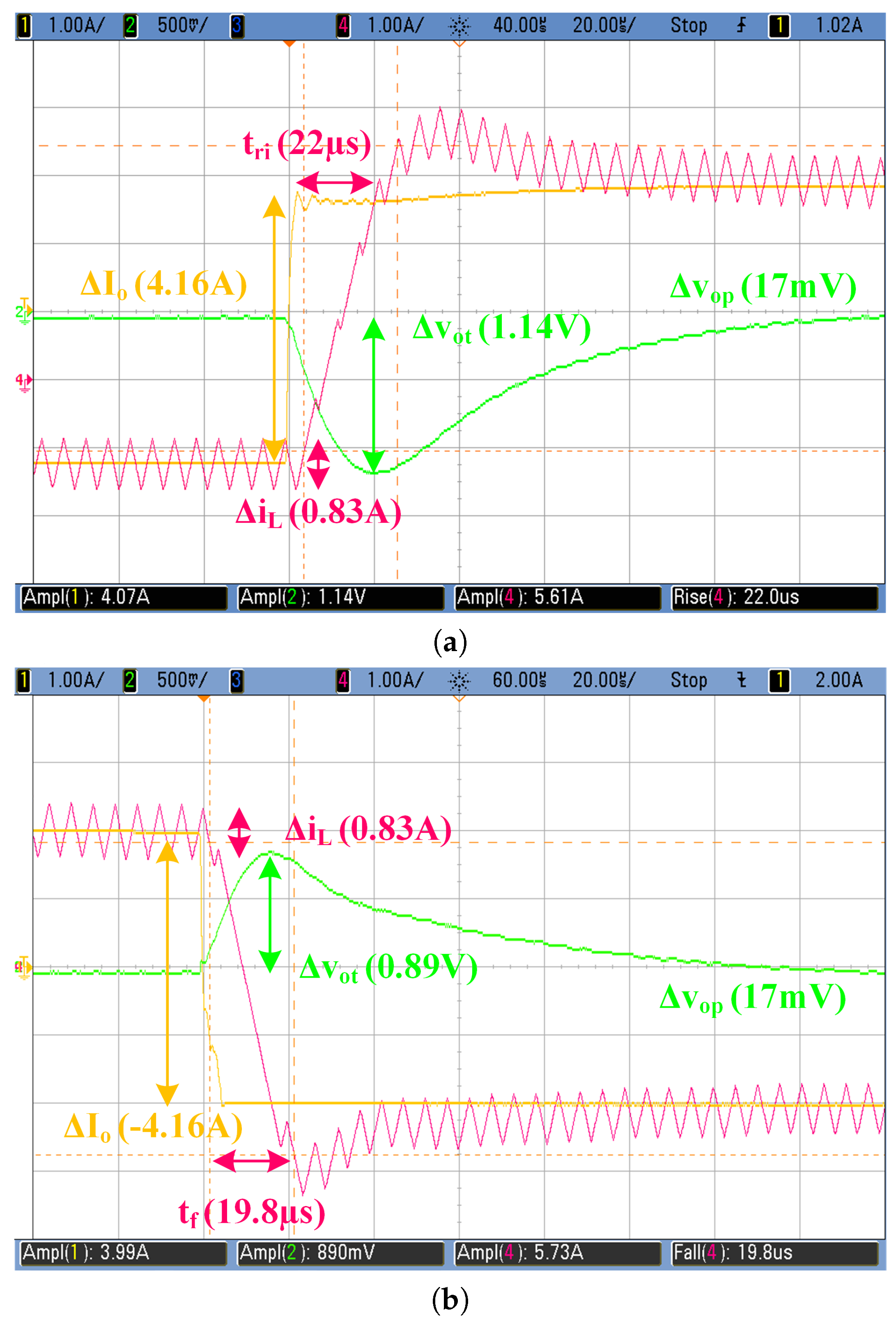
In order to test the assembled BP, two different experiments have been carried out. The first one is related to the QoS of the proposed architecture in this work. In this case, the maximum current steps are performed and the dynamic response of the BP has been measured; see
Figure 9. These loads steps (
) are established by the QoS as ±4.16 A. More precisely, the sink to source step is depicted in
Figure 9a. As can be seen, after the load step, the duty cycle is limited to 0.9; hence, the dynamic response is also limited by the inductance value, which determines the increase of current and output capacitor value. The latter has to provide the amount of power demanded by the load during the transient. In this case, the measured voltage drop is 1.14 V. This value is below the requirement fixed in the standard, which was 1.2 V. The measured steady state error is around 17 mV, far below the maximum allowed by the QoS.
The results obtained for source to sink transition can be seen in
Figure 9b. The same conclusions can be derived from this transient. In this particular case, the output capacitor is charged with the excessive amount of energy provided by the load during the transient. The measured over-voltage is around 0.89 V and the steady state error is the same as in the sink to source transient (17 mV). Both measurements are below the limits of the QoS.
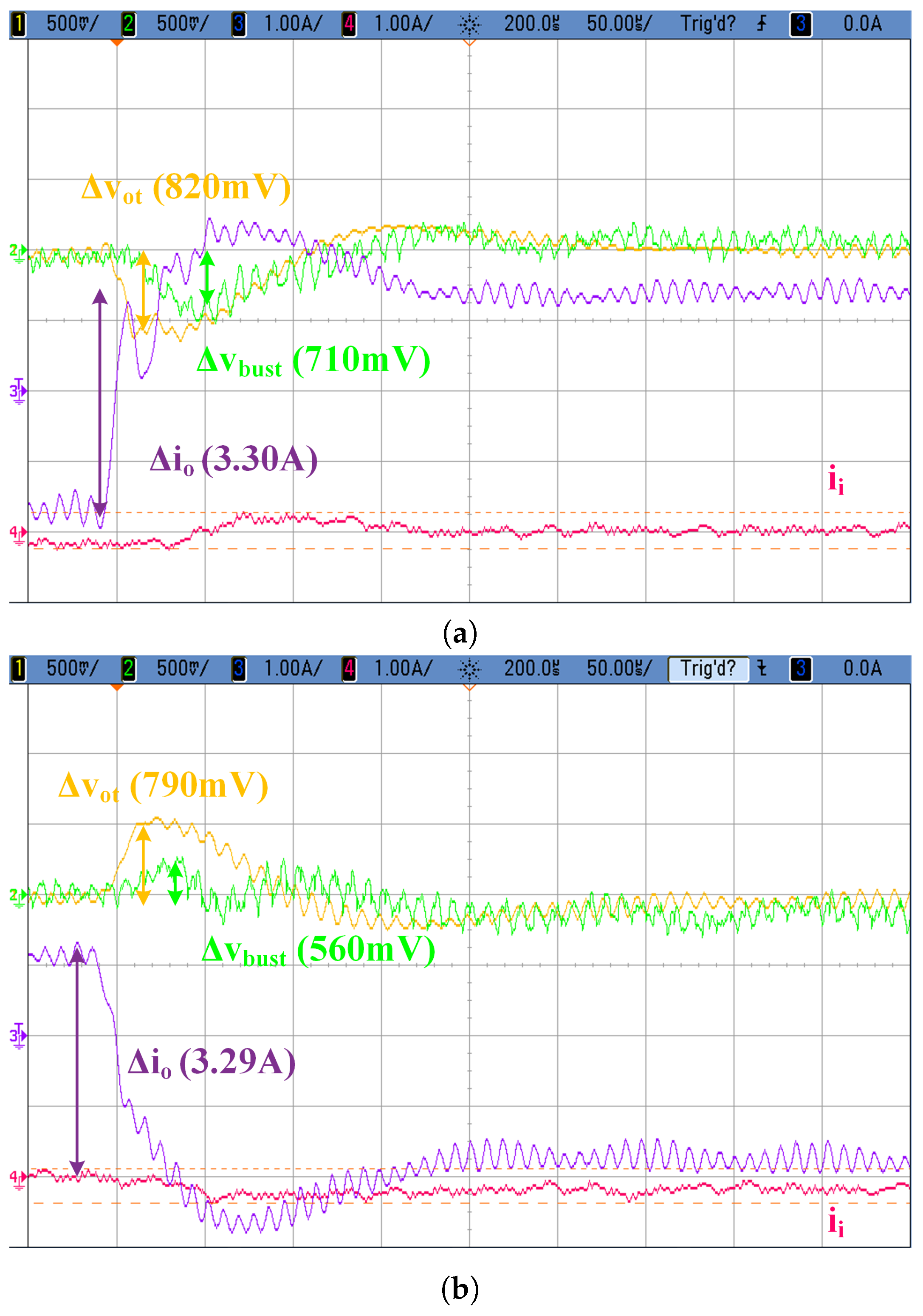
The second test has been run to demonstrate the flexibility of the BP and its capacity to deal with bidirectional power flows following the proposed standard regulations. For this purpose, a custom made PoL power converter was built in the laboratory for stepping down the voltage from 24 V to 12 V, ±100 W and with an input capacitor of 75 μF. Two different scenarios are proposed using this PoL.
In the first scenario, several passive loads are connected to channel 2, demanding the maximum power (i.e., 100 W). Two active loads of −50 W each are connected to channels 3 and 4, respectively. No load is connected to channel 5 and a load step from −40 W to 40 W and vice versa is performed in channel 1. In all cases, the passive and active loads are interfaced by the PoL converter mentioned. The measured waveforms are depicted in
Figure 10, where
refers to the internal 48 V bus and
is the input current of the BP. The results obtained for −40 W to 40 W load step can be observed in
Figure 10a. As in the previous case, it can be seen how the BP regulates the 48 V internal bus as well as the 24 V bus within the limits established by the QoS. The similar conclusion can be extracted when looking at the measurements of 40 W to −40 W load step (see
Figure 10b). This transition illustrates how the BP is able to sink current from the 24 V bus to the high voltage DC bus (380 V bus) without the use of the droop control technique.
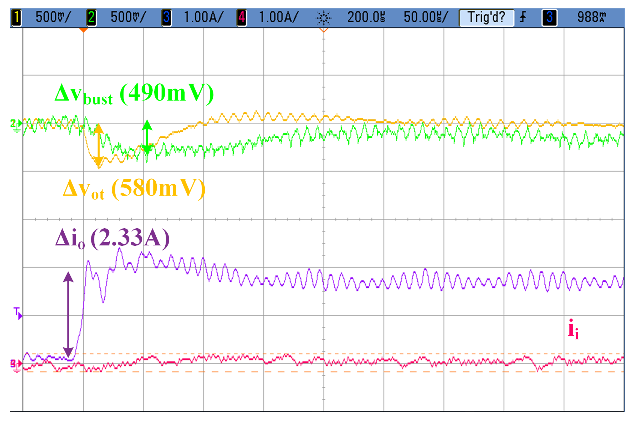
In the second scenario, the same set up is performed for channels 2, 3 and 4, whilst a passive load demanding 50 W is connected to channel 1. Therefore, in
Figure 11, the load step of the BP when no power is being transferred to provide 50 W can be observed. As in the previous scenario, the over voltages and steady state errors fall within the boundaries of the proposed QoS. These experimental results validate the proposed algorithm of design and they also demonstrate the viability of the proposed architecture.
6. Conclusions
In this paper, the bidirectional power flow in DC nano-grids has been analyzed. First, a two bus power architecture has been chosen as the most promising DC distribution system. In terms of power losses and user safety, the combination of a high voltage, high power DC bus (380 V) with a low voltage, low power DC bus (24 V) has several advantages over a single high voltage distribution or a lower DC voltage. The main drawback of this power architecture is the need for load classification: those which can draw more than 100 W and those which demand a lower power level. This restricts the end-user flexibility to connect a load either to the 380 V bus or to the 24 V bus. However, most domestic loads fall in either category, minimizing this potential issue.
Second, a possible bus standard has been proposed for domestic, bidirectional DC nano-grids. This proposal defines a basic QoS based on some parameters regarding DC voltage regulation, such as the steady state error or the maximum over voltage during transients. Several technical recommendations have been followed and it is applicable to active and passive load connections.
Finally, a BP has also been proposed. In this work, a single-input, multiple output bidirectional BP based on a DAB and five buck converters is studied as a potential power converter to meet the QoS. The key design aspects have been also pointed out:
A simple power flow control mechanism is proposed to reduce regulator complexity and avoid using droop control.
Considering loop control degradation due to load converter impedances helps design the BP output filters and regulators to ensure QoS compliance.
Different control techniques for the buck converter are considered, highlighting their advantages and disadvantages for different scenarios.
The DAB transformer is designed to ensure ZVS operation even at no load, enhancing its performance when the user does not connect any elements to the bus.
The experimental measurements of expected user behaviors demonstrate the technical viability of the proposed BP and the use of the QoS to properly design this power converter.
Author Contributions
Conceptualization, J.S.; funding acquisition, M.A. and J.S.; investigation, A.V. and K.M.; methodology, A.V. and K.M.; supervision, J.S.; validation, A.V. and K.M., writing—original draft, A.V.; writing—review and editing, A.V., K.M. and M.A.
Funding
This work was supported in part by the Spanish Government under projects MINECO-17-DPI2016-75760-R and RTI2018-099682-A-I00; in part by the Principality of Asturias under project IDI/2018/000179 and Severo Ochoa grant BP14-085; and in part by the European Regional Development Fund Grants (FEDER).
Conflicts of Interest
The authors declare no conflict of interest.
Abbreviations
The following abbreviations are used in this manuscript:
| BMS | Battery Management System |
| BP | Bus Provider |
| DAB | Dual Active Bridge |
| ESS | Energy Storage System |
| FPGA | Field Programmable Gate Array |
| HV | High Voltage bus |
| LV | Low Voltage bus |
| MPPT | Maximum Power Point Tracker |
| PF | Power Factor |
| PoL | Point of Load power converter |
| QoS | Quality of Service |
| RES | Renewable Energy Sources |
| RHPZ | Right Half Plane Zero |
| THDi | Current Total Harmonic Distortion |
| UPS | Uninterruptible Power Supply |
| ZVS | Zero Voltage Switching |
References
- Brown, C. Charging for electricity in the early years of electricity supply. IEE Proc. A Phys. Sci. Meas. Instrum. Manag. Educ. Rev. 1985, 132, 513. [Google Scholar] [CrossRef]
- Blaabjerg, F.; Chen, Z.; Kjaer, S.B. Power electronics as efficient interface in dispersed power generation systems. IEEE Trans. Power Electron. 2004, 19, 1184–1194. [Google Scholar] [CrossRef]
- Nonogaki, M.; Kikuchi, T.; Keiichi, H.; Hidenori, M.; Takashi, T. Development of the mutual energy exchanging system between areas by the direct-current system which utilized renewable energy. In Proceedings of the 2014 IEEE 36th International Telecommunications Energy Conference (INTELEC), Vancouver, BC, Canada, 28 September–2 October 2014; pp. 1–6. [Google Scholar] [CrossRef]
- Boroyevich, D.; Cvetković, I.; Dong, D.; Burgos, R.; Wang, F.; Lee, F. Future electronic power distribution systems—A contemplative view. In Proceedings of the 2010 12th International Conference on Optimization of Electrical and Electronic Equipment, Basov, Romania, 20–22 May 2010; pp. 1369–1380. [Google Scholar] [CrossRef]
- Power Division of the IEE. Fifth International Conference on AC and DC Power Transmission: 17–20 September 1991, London. In Proceedings of the International Conference on AC and DC Power Transmission, London, UK, 17–20 September 1991; Institution of Engineering & Technology: London, UK, 1991; p. 427.
- Liu, X.; Su, B. Microgrids—An integration of renewable energy technologies. In Proceedings of the 2008 China International Conference on Electricity Distribution, Guangzhou, China, 10–13 December 2008; pp. 1–7. [Google Scholar]
- Wunder, B.; Kaiser, J.; Fersterra, F.; Ott, L.; Han, Y.; Marz, M. Energy distribution with DC microgrids in commercial buildings with power electronics. In Proceedings of the 2015 IEEE International Symposium on Smart Electric Distribution Systems and Technologies (EDST), Vienna, Austria, 8–11 September 2015; pp. 425–430. [Google Scholar] [CrossRef]
- Becker, D.J.; Sonnenberg, B.J. DC microgrids in buildings and data centers. In Proceedings of the 2011 IEEE 33rd International Telecommunications Energy Conference (INTELEC), Amsterdam, The Netherlands, 9–13 October 2011; pp. 1–7. [Google Scholar] [CrossRef]
- Sannino, A.; Postiglione, G.; Bollen, M.H. Feasibility of a DC network for commercial facilities. IEEE Trans. Ind. Appl. 2003, 39, 1499–1507. [Google Scholar] [CrossRef]
- Daolian, C. Present states and development of the single-Stage uninterruptible AC–DC converters. In Proceedings of the 2009 Twenty-Fourth Annual IEEE Applied Power Electronics Conference and Exposition, Washington, DC, USA, 15–19 February 2009; pp. 1915–1918. [Google Scholar] [CrossRef]
- Arias Pérez de Azpeitia, M.; Fernández, A.; Lamar, D.G.; Rodríguez, M.; Hernando, M.M. Simplified voltage-sag filler for line-interactive uninterruptible power supplies. IEEE Trans. Ind. Electron. 2008, 55, 3005–3011. [Google Scholar] [CrossRef]
- Kakigano, H.; Miura, Y.; Ise, T.; Uchida, R. DC micro-grid for super high quality distribution—System configuration and control of distributed generations and energy storage devices. In Proceedings of the 2006 37th IEEE Power Electronics Specialists Conference, Jeju, Korea, 18–22 June 2006; pp. 1–7. [Google Scholar] [CrossRef]
- Mackay, L.; Ramirez-Elizondo, L.; Bauer, P. DC ready devices—Is redimensioning of the rectification components necessary? In Proceedings of the 16th International Conference on Mechatronics-Mechatronika, Brno, Czech Republic, 3–5 December 2014; pp. 1–5. [Google Scholar] [CrossRef]
- Kakigano, H.; Miura, Y.; Ise, T. Distribution voltage control for DC microgrids using fuzzy control and gain-scheduling technique. IEEE Trans. Power Electron. 2013, 28, 2246–2258. [Google Scholar] [CrossRef]
- Weiss, R.; Ott, L.; Boeke, U. Energy efficient low-voltage DC-grids for commercial buildings. In Proceedings of the 2015 IEEE First, International Conference on DC Microgrids (ICDCM), Atlanta, GA, USA, 7–10 June 2015; pp. 154–158. [Google Scholar] [CrossRef]
- Aalborg University. Intelligent DC Microgrid Living Lab; Aalborg University: Alaborg, Denmark, 2019. [Google Scholar]
- USB Implementers Forum. USB Power Delivery Specification; Technical Report Std., Rev. 2.0 v1.3; USB Implementers Forum: Beaverton, OR, USA, 2017. [Google Scholar]
- Daft. List of the Power Consumption of Typical Household Appliances. Available online: https://www.daftlogic.com/information-appliance-power-consumption.htm (accessed on 28 September 2018).
- Charlton Lights. LED Light Requirement Calculator. Available online: http://www.charlstonlights.com/led-light-requirement-calculator (accessed on 28 September 2018).
- Middlebrook, R. Input filter considerations in design and application of switching regulators. IEEE Ind. Appl. Soc. Annu. Meet. Rec. IEEE 1976, 1976, 366–382. [Google Scholar]
- Sokal, N. System oscillations caused by negative input resistance at the power input port of a switching mode regulator, amplifier, DC/DC converter, or DC/ac inverter. In Proceedings of the 1973 IEEE Power Electronics Specialists Conference, Pasadena, CA, USA, 11–13 June 1973. [Google Scholar]
- Schönberger, J.; Duke, R.; Round, S.D. DC-bus signaling: A distributed control strategy for a hybrid renewable nanogrid. IEEE Trans. Ind. Electron. 2006, 53, 1453–1460. [Google Scholar] [CrossRef]
- Rodríguez, M.; Stahl, G.; Corradini, L.; Maksimović, D. Smart DC power management system based on software-configurable power modules. IEEE Trans. Power Electron. 2013, 28, 1571–1586. [Google Scholar] [CrossRef]
- Guerrero, J.M.; Vasquez, J.C.; Matas, J.; De Vicuña, L.G.; Castilla, M. Hierarchical control of droop-controlled AC and DC microgrids—A general approach toward standardization. IEEE Trans. Ind. Electron. 2011, 58, 158–172. [Google Scholar] [CrossRef]
- Dragicevic, T.; Guerrero, J.M.; Vasquez, J.C.; Skrlec, D. Supervisory control of an adaptive-droop regulated DC microgrid with battery management capability. IEEE Trans. Power Electron. 2014, 29, 695–706. [Google Scholar] [CrossRef]
- Nasirian, V.; Moayedi, S.; Davoudi, A.; Lewis, F.L. Distributed cooperative control of DC microgrids. IEEE Trans. Power Electron. 2015, 30, 2288–2303. [Google Scholar] [CrossRef]
- Ham, J. MIL EMI and Transient Solutions; Technical Report Application Note AN:022; Vicor Corporation: Andover, MA, USA, 2007. [Google Scholar]
- ETSI. Power Supply Interface at the Input to Telecommunications and Datacom (ICT) Equipment; Part 2: Operated by by -48 V Direct Current (DC); Technical Report EN 300 132-2 V2.1.1., ETSI Std., Rev. 2.1.1; ETSI: Sophia Antipolis, France, 2012. [Google Scholar]
- King, B. Design Considerations for USB Type-C Power Delivery; Texas Instruments: Dallas, TX, USA, 2018. [Google Scholar]
- Krismer, F. Modeling and Optimization of Bidirectional Dual Active Bridge AC–DC Converter Topologies. Ph.D. Thesis, ETH Zurich, Zurich, Switzerland, 2010. [Google Scholar] [CrossRef]
- Kheraluwala, M.; Gascoigne, R.; Divan, D.; Baumann, E. Performance characterization of a high-power dual active bridge DC-to-DC converter. IEEE Trans. Ind. Appl. 1992, 28, 1294–1301. [Google Scholar] [CrossRef]
- Martin, K.; Vázquez, A.; Arias, M.; Sebastián, J. Optimization procedure of source/sink converters for DC power distribution nano-grids. In Proceedings of the 2018 IEEE 19th Workshop on Control and Modeling for Power Electronics (COMPEL), Padua, Italy, 25–28 June 2018; pp. 1–8. [Google Scholar] [CrossRef]
- Arbetter, B.; Maksimović, D. Feedforward pulse width modulators for switching power converters. IEEE Trans. Power Electron. 1997, 12, 361–368. [Google Scholar] [CrossRef]
- Redl, R.; Sokal, N.O. Current-mode control, five different types, used with the three basic classes of power converters: Small-signal AC and large-signal DC characterization, stability requirements, and implementation of practical circuits. In Proceedings of the IEEE Power Electronics Specialists Conference, Toulouse, France, 24–28 June 1985; pp. 771–785. [Google Scholar] [CrossRef]
- Dixon, L.H. Average Current Mode Control of Switching Power Supplies; Technical Report Application Note U-140; Unitrode Corp: Merrimack, NH, USA, 1990. [Google Scholar]
- Smedley, K.; Cuk, S. One-cycle control of switching converters. In Proceedings of the PESC ’91 Record 22nd Annual IEEE Power Electronics Specialists Conference, Cambridge, MA, USA, 24–27 June 1991; pp. 888–896. [Google Scholar] [CrossRef]
- Ma, D.; Ki, W.H.; Tsui, C.Y. A fast response adaptive DC–DC switching converter using on-chip dual-loop one-cycle control. In Proceedings of the 28th European Solid-State Circuits Conference, Florence, Italy, 24–26 September 2002; pp. 379–382. [Google Scholar]
- Vorperian, V. Quasi-square-wave converters: Topologies and analysis. IEEE Trans. Power Electron. 1988, 3, 183–191. [Google Scholar] [CrossRef]
- Marxgut, C.; Biela, J.; Kolar, J.W. Interleaved Triangular Current Mode (TCM) resonant transition, single phase PFC rectifier with high efficiency and high power density. In Proceedings of the 2010 International Power Electronics Conference—ECCE ASIA, Sapporo, Japan, 21–24 June 2010; pp. 1725–1732. [Google Scholar] [CrossRef]
- Riedel, J.; Holmes, D.G.; McGrath, B.P.; Teixeira, C. ZVS soft switching boundaries for dual active bridge DC–DC converters using frequency domain analysis. IEEE Trans. Power Electron. 2017, 32, 3166–3179. [Google Scholar] [CrossRef]
- Shen, Z.; Burgos, R.; Boroyevich, D.; Wang, F. Soft-switching capability analysis of a dual active bridge DC–DC converter. In Proceedings of the 2009 IEEE Electric Ship Technologies Symposium, Baltimore, MD, USA, 20–22 April 2009; pp. 334–339. [Google Scholar] [CrossRef]
- Hiltunen, J.; Vaisanen, V.; Juntunen, R.; Silventoinen, P. Variable-Frequency Phase Shift Modulation of a Dual Active Bridge Converter. IEEE Trans. Power Electron. 2015, 30, 7138–7148. [Google Scholar] [CrossRef]
- Higa, H.; Itoh, J.I. Extension of zero-voltage-switching range in dual active bridge converter by switched auxiliary inductance. In Proceedings of the 2017 IEEE Energy Conversion Congress and Exposition (ECCE), Cincinnati, OH, USA, 1–5 October 2017; pp. 5324–5331. [Google Scholar] [CrossRef]
- Nan, C.; Ayyanar, R. Dual active bridge converter with PWM control for solid state transformer application. In Proceedings of the 2013 IEEE Energy Conversion Congress and Exposition, Denver, CO, USA, 15–19 September 2013; pp. 4747–4753. [Google Scholar] [CrossRef]
- Rodriguez, A.; Vazquez, A.; Lamar, D.G.; Hernando, M.M.; Sebastian, J. Different Purpose Design Strategies and Techniques to Improve the Performance of a Dual Active Bridge With Phase-Shift Control. IEEE Trans. Power Electron. 2015, 30, 790–804. [Google Scholar] [CrossRef]
- Segaran, D.; Holmes, D.G.; McGrath, B.P. Enhanced load step response for a bidirectional DCDC converter. IEEE Trans. Power Electron. 2013, 28, 371–379. [Google Scholar] [CrossRef]
- Erickson, R.W.; Maksimovic, D. Regulator Design. In Fundamentals of Power Electronics, 2nd ed.; Kluwer: New York, NY, USA, 2001; Chapter 9; pp. 347–654. [Google Scholar]
Figure 1.
Traditional single-phase AC distribution in a household. Some loads are depicted as an example of potential consumers in the grid.
Figure 1.
Traditional single-phase AC distribution in a household. Some loads are depicted as an example of potential consumers in the grid.
Figure 2.
Different possible connections of the renewable energy systems (RES) to an AC grid. (a) without energy storage system (ESS); (b) with an ESS in AC; (c) with an ESS in DC. The bidirectional power converters are highlighted in grey.
Figure 2.
Different possible connections of the renewable energy systems (RES) to an AC grid. (a) without energy storage system (ESS); (b) with an ESS in AC; (c) with an ESS in DC. The bidirectional power converters are highlighted in grey.
Figure 3.
Single DC bus distribution for a household. The bidirectional power converters are highlighted in grey.
Figure 3.
Single DC bus distribution for a household. The bidirectional power converters are highlighted in grey.
Figure 4.
DC distribution system based on two DC buses: a high voltage DC bus (HV) and a low voltage DC bus (LV) interconnected by an isolated DC–DC power converter, known as bus provider (BP).
Figure 4.
DC distribution system based on two DC buses: a high voltage DC bus (HV) and a low voltage DC bus (LV) interconnected by an isolated DC–DC power converter, known as bus provider (BP).
Figure 5.
Proposed DC distribution based on two buses with a bidirectional bus provider.
Figure 5.
Proposed DC distribution based on two buses with a bidirectional bus provider.
Figure 6.
Bus provider possible implementation: a Dual Active Bridge (DAB) cascaded with five synchronous buck converters.
Figure 6.
Bus provider possible implementation: a Dual Active Bridge (DAB) cascaded with five synchronous buck converters.
Figure 7.
Comparison of different control strategies for the synchronous buck converter.
Figure 7.
Comparison of different control strategies for the synchronous buck converter.
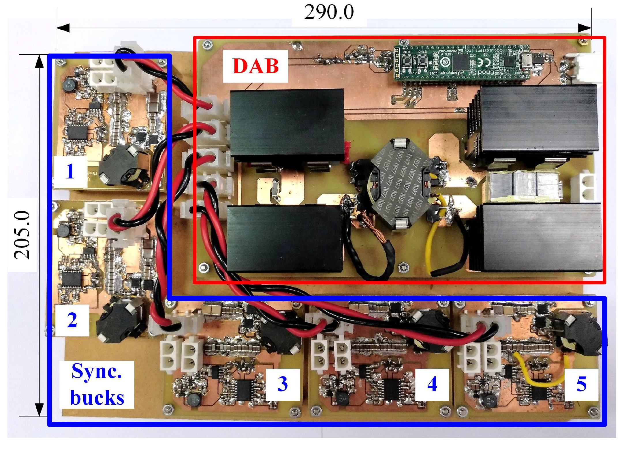
Figure 8.
Proposed Bus Provider (BP) built in the lab composed of a DAB and five synchronous buck converters, dimensions in mm.
Figure 8.
Proposed Bus Provider (BP) built in the lab composed of a DAB and five synchronous buck converters, dimensions in mm.
Figure 9.
Buck converter response against the maximum load steps. Ch1: Output current (), 1 A/div. Ch2: Output voltage (), 500 mV/div, (AC). Ch3: Current through the inductance (), 1 A/div. Time division: 20 μs/div. (a) from −1.2 A to 3.0 A; (b) from 2.1 A to −2.1 A.
Figure 9.
Buck converter response against the maximum load steps. Ch1: Output current (), 1 A/div. Ch2: Output voltage (), 500 mV/div, (AC). Ch3: Current through the inductance (), 1 A/div. Time division: 20 μs/div. (a) from −1.2 A to 3.0 A; (b) from 2.1 A to −2.1 A.
Figure 10.
Experimental results for the BP under source sink load steps. Ch1: , 500 mV/div (AC). Ch2: , 500 mV/div (AC). Ch3: , 1 A/div. Ch4: , 1 A/div. Time scale: 200 μs/div. (a) load step from −40 W to 40 W; (b) load step from 40 W to −40 W.
Figure 10.
Experimental results for the BP under source sink load steps. Ch1: , 500 mV/div (AC). Ch2: , 500 mV/div (AC). Ch3: , 1 A/div. Ch4: , 1 A/div. Time scale: 200 μs/div. (a) load step from −40 W to 40 W; (b) load step from 40 W to −40 W.
Figure 11.
Experimental results for the BP under no load to source mode, 0 W to 50 W. Ch1: , 500 mV/div (AC). Ch2: , 500 mV/div (AC). Ch3: , 1 A/div. Ch4: , 1 A/div. Time scale: 200 μs/div.
Figure 11.
Experimental results for the BP under no load to source mode, 0 W to 50 W. Ch1: , 500 mV/div (AC). Ch2: , 500 mV/div (AC). Ch3: , 1 A/div. Ch4: , 1 A/div. Time scale: 200 μs/div.
Table 1.
Classification of typical household loads according to the demanded power.
Table 1.
Classification of typical household loads according to the demanded power.
| Low Power Loads | Fixed Loads P > 100 W | Portable Loads P > 100 W |
|---|
| Laptop | 20–60 W | Refrigerator | 150–350 W | Iron | 750–1100 W |
| Reading lamp | 10–15 W | Dishwasher | 1200 W | Vacuum cleaner | 650–800 W |
| LED lamp | 10–50 W | Microwave oven | 1500 W | Hair dryer | 300–600 W |
| Cell phone charger | 5 W | Electric oven | 2500 W | Drill | 1000 W |
| Electric shaver | 5–15 W | Washer | 2000 W | Hair straightener | 50–300 W |
| Router | 7–10 W | Dryer | 5000 W | Beater | 250–350 W |
| LED TV screen | 20–60 W | PC | 150–400 W | Toaster | 1200 W |
Table 2.
Synchronous buck converter parameters with the proposed design.
Table 2.
Synchronous buck converter parameters with the proposed design.
| Parameter | Value |
|---|
| Transistors | FDB3502, On Semiconductor
75 V, 14 A, 47 mΩ, D2PAK |
| Core and magnetic material | RM8, N97 EPCOS |
| Switching frequency, [kHz] | 183.5 |
| Controller | Analog, MC33023, On Semiconductor |
| L [μH] | 78.5 |
| [μF] | 39 |
| [μF] | 3 |
| Voltage feedback loop bandwidth, [kHz] | 14.6 |
| Compensator | Type III, PM 51.66 deg |
| Inductor losses, [W] | 0.41 |
| Transistor losses, [W] | 1.73 |
| Control and driving losses, [W] | 0.51 |
| [W] | 2.65 |
Table 3.
DAB parameters with the proposed design.
Table 3.
DAB parameters with the proposed design.
| Parameter | Value |
|---|
| Transistors (primary) | TW18N60DM2, ST Microelectronics
600 V, 12 A, 260 mΩ, TO247 |
| Transistors (secondary) | IRFB3806PbF, Infineon
60 V, 43 A, 15.8 mΩ, TO220 |
| Core and magnetic material | RM14, N97 EPCOS |
| [kHz] | 123.9 |
| [turns] | 48 |
| [turns] | 6 |
| [μH] | 206.1 |
| [μH] | 720.6 |
| Controller | Digital, FPGA Spartan 6, Xilinx, CMODS6 |
| [μF] | 10 |
| [μF] | 3 |
| [W] | 2.54 |
| [W] | 11.33 |
| [W] | 0.32 |
| [W] | 14.10 |
© 2019 by the authors. Licensee MDPI, Basel, Switzerland. This article is an open access article distributed under the terms and conditions of the Creative Commons Attribution (CC BY) license (http://creativecommons.org/licenses/by/4.0/).


