1. Introduction
With the growing level of power density in up-to-date power devices and assemblies, it has become essential to support their manufacturing with testing tools enabling one to check the integrity of the realized appliances. There are several existing traditional non-destructive analysis techniques, such as x-ray or scanning acoustic microscopy (SAM), but their use is troublesome and may require the assembly to be dismounted, at least partly. There is a growing need to provide an appropriate testing methodology that can be used for in situ analysis of power devices and which is not restricted to checking just a certain part within the assembly. It is also often expected that after verifying the correctness of the design or the integrity of a sample by thermal testing, the product remains functional in its normal operation mode.
In literature we can find ways to use thermal transients induced by power change to characterize a part of an electronic appliance. Recognizing that the thermal transient testing always provides information about the whole heat conducting path from a heat source towards the measurement environment, in this paper we systematically follow the possibilities for analyzing complex structures built from power electronics devices, thermal interface materials, and cooling mounts.
The theoretical principles of structural transient testing are summarized in previous studies, such as [
1,
2,
3]. In this paper we examine a series of examples of how this technique can be used for analyzing the health of the different structural elements at different locations in the assembly.
In many cases the structural analysis is simplified to condensing the detailed composition of the device into a single characteristic number. Such often used descriptors are the RthJC junction to case thermal resistance for devices with a dedicated cooling surface (“case”) or the RthJA junction to ambient thermal resistance for assemblies. These data are useful for narrowing the selection of devices for an engineering task and for “back of the envelope” calculations but do not replace trial measurements and simulations for an actual design.
The well-established framework of thermal measurement standards [
4,
5,
6], however, helps in planning the structural analysis process as well. These standards represent the condensed knowledge of many decades regarding the selection of assemblies, thermal boundary, electrical excitation, data acquisition, and the interpretation of the measured results.
The traditional standards and methods are highly based on the characteristic features of the silicon material used in power switching and amplifying appliances. Testing of silicon devices in regular packages more or less goes through a checklist. However, when these methods were used for large area power modules, containing several functional dice, some of the results proved to be inappropriate [
7]. With the advent of the use of wide band-gap materials, many of the established testing methods have become impractical or even misleading [
8].
In this paper, we will introduce cases where a sort of “Design of Experiment” is needed, although not in the broadest statistical sense. Instead, a proper re-interpretation of the standard framework has to be applied, involving trials on powering and sensing currents. In addition, standards give only detailed support for cases when the analyzed part of the assembly is the heat conducting path from the semiconductor to a physical package surface. If the part of interest in the assembly is another structural element, such as a thermal interface material (TIM) layer or a cooling mount, a proper re-definition of the methodology is needed.
It has to be noted that although thermal testing has become more important in achieving reliable operation over a long lifetime, the construction of complete appliances often overlooks thermal testability aspects. Consequently, these tests often need a workaround for accessing devices that are relevant for their power consumption or can be used as sensing points.
In the following sections we follow the steps of how thermal transient testing can be used for structure analysis. First, in
Section 2, we present how the thermal transient testing can be accomplished in practice. In
Section 3, we discuss how the measured results can be interpreted in structure analysis.
Section 4 presents various case studies, with each demonstrating a special interpretation of the structure functions, depending on our knowledge of the actual structure. These examples also allow us to demonstrate how the difficulties in the thermal transient evaluation of these devices can be overcome. Finally, in
Section 5 we summarize the findings and give recommendations about using thermal transient testing for structure analysis.
2. Thermal Transient Measurements
Generally, to carry out thermal transient measurements we need one or more heater elements and one or several temperature sensors. In most cases the heat source is a semiconductor, typically called the “chip” in the literature on system design and the “die” (plural dice, sometimes dies) in works on semiconductor technology and packaging. As defined in measurement standards [
4,
5], in discrete devices that have a solitary die, the powering and sensing can occur on the same device; more precisely, on its dissipating surface. In this way we can record the temperature change of the hottest point in an electronic circuitry.
In thermal measurements the traditional term “junction” is often used for the powered thin material layer of the semiconductor. In many device categories (diodes, insulated gate transistors, thyristors) the heat source that is also serving as the sensor is in fact a pn junction driven into forward operation.
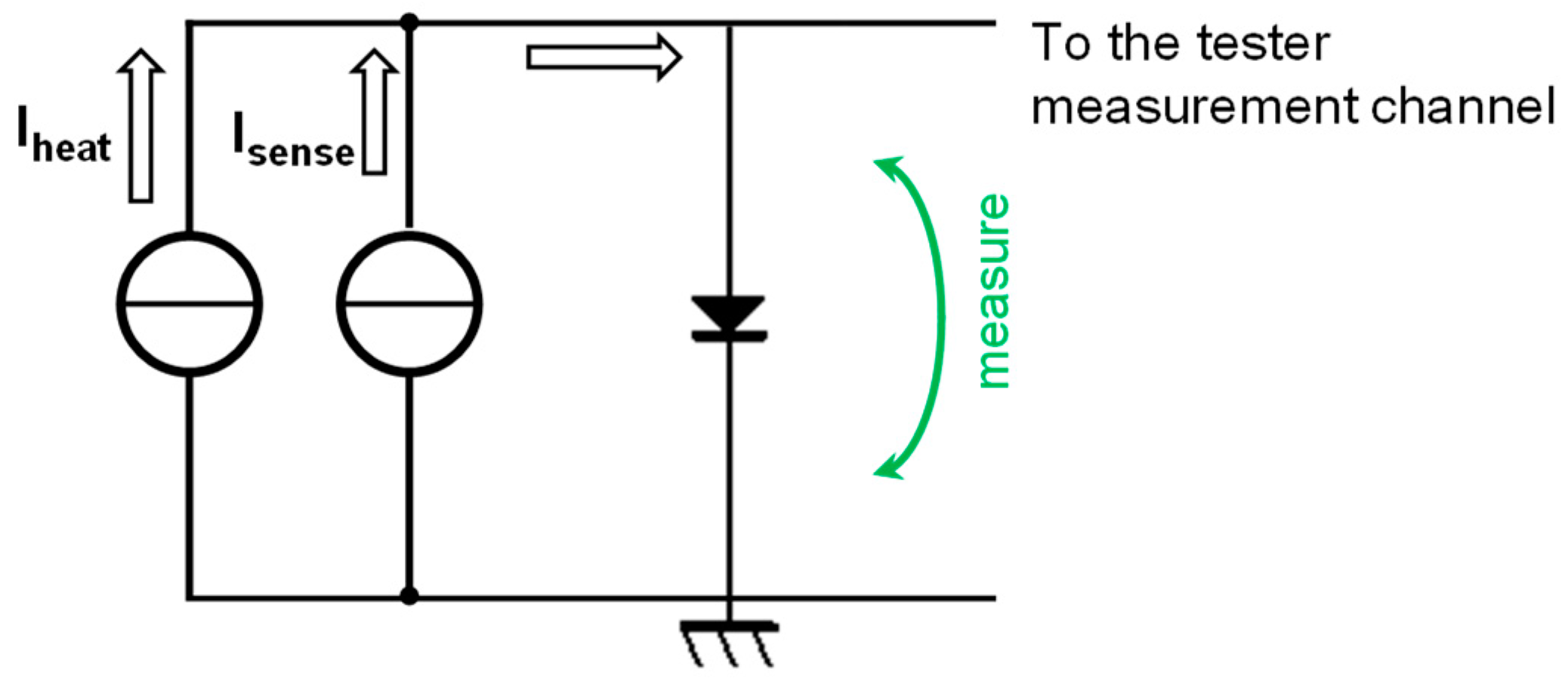
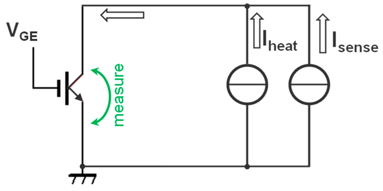
The required sudden power change on a pn junction can be created by switching down from a high
IHEAT heating current to a low
ISENSE measurement current level (
Figure 1).
The sensing current maintains a forward voltage on the device at a low power level. In a calibration step, this voltage can be mapped to the junction temperature. This is achieved by recording the voltage in a thermostat at different temperatures, using the same low current.
In the case of modules, the heating current(s) may flow through several devices, and more dice can be used for sensing, applying a sensor current on each of them. Many details of the powering and temperature sensing principles are given in a previous study [
9].
2.1. Test Definition
Structural analysis by thermal transient testing is a robust technique, covering a very wide range of devices. The same principles and practical methods are valid for microelectro-mechanical systems (MEMS), locomotive engine drives, or processors. The range of applied heating currents is milliamperes for MEMS and kiloamperes for engine drives; the time for reaching thermal equilibrium is milliseconds for MEMS and hours for street luminaires, although the same methodology still applies.
As stated above, measurement standards offer appropriate guidelines for a test framework.
The JEDEC JESD 51-14 thermal transient measurement standard prescribes the careful definition of the
device type,
environmental conditions,
powering, and
data acquisition conditions, and
data evaluation (
Table 1 in the reference [
6]).
Thermal testing and the evaluation of the results could be treated in a purely theoretical way, but it is easier to understand the concepts through a practical example. In this work, we present measurements on six quite different devices, each of which could be used as device type to expose the general principles. We present now the test of a typical high current module, a solid state relay. We have already used this device as a workhorse to present the thermal management concepts because of its ruggedness and flexibility in other works [
10,
11], but with a different focus. Now, after using it as an example for introducing the basic measurements in
Section 2, we concentrate on its special features for the uses of a high sense current (
Section 3.3), low heating current (
Section 3.3 and
Section 4.6), and the roughness of its base plate, which necessitates a curing step when used with thermal interface pastes (
Section 4.5).
The test definition is as follows.
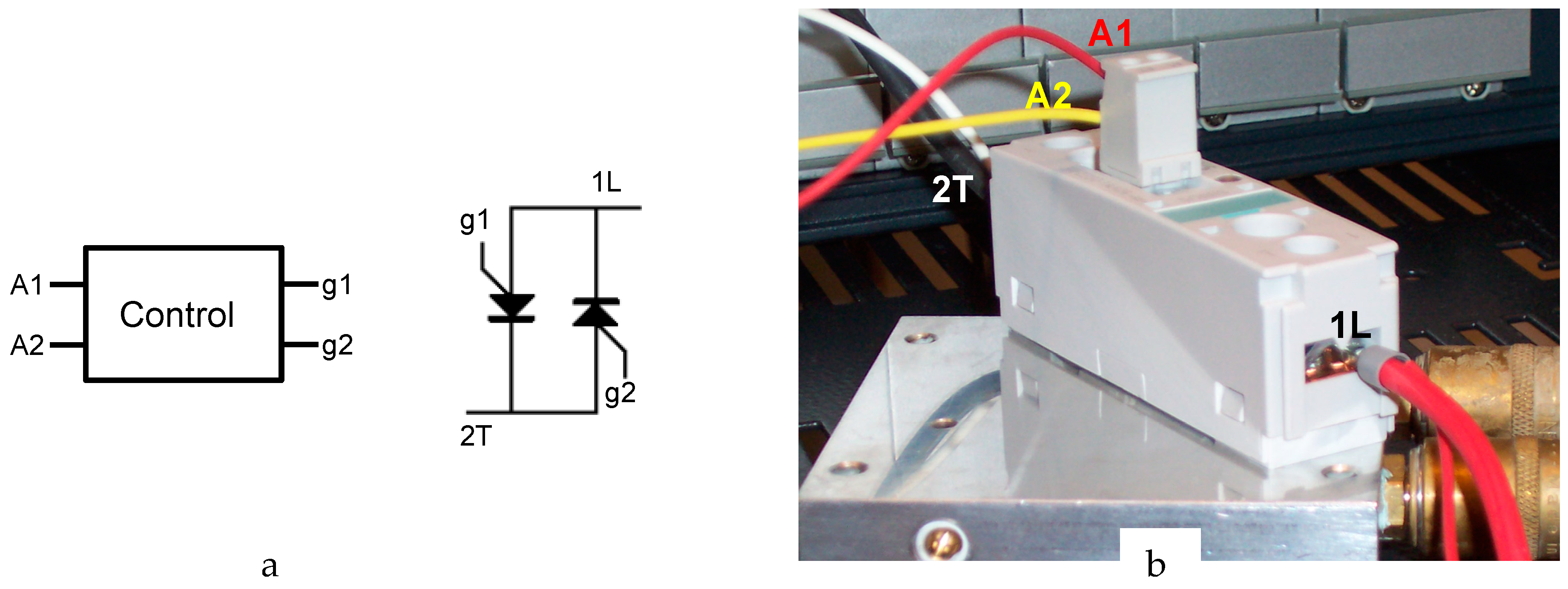
Device type: standard Siemens AC solid state relay module, type 3RF2190. The module contains two thyristors (Silicon Controlled Rectifier (SCR)) and some control circuitry on a ceramic direct bonded copper (DBC) substrate. A simplified schematic of the device is shown in
Figure 2a.
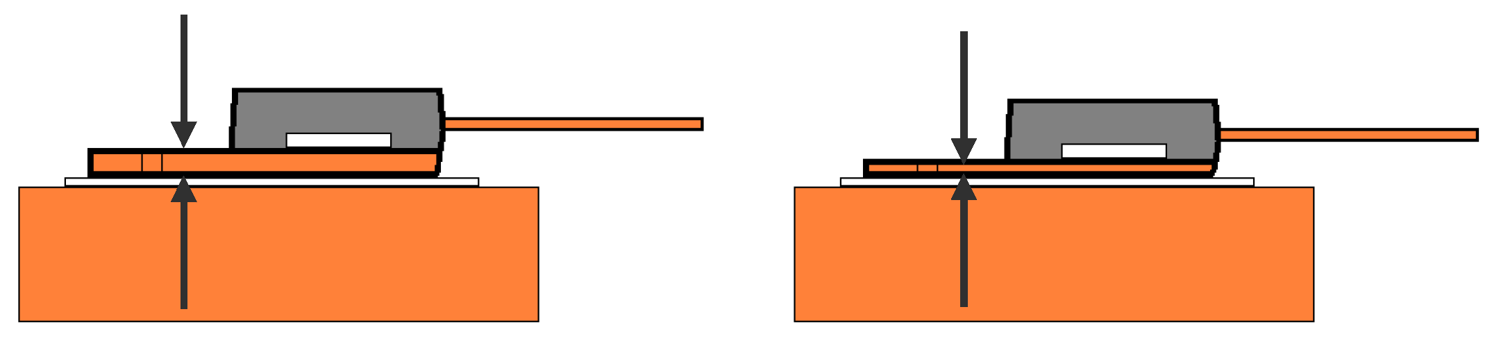
Assembly and environment: The samples were fixed on a water cooled cold-plate, with different thermal interfaces underneath. In order to distinguish between the portions of the heat conducting path belonging to the device, the TIM, and the cooling mount, we followed the JEDEC JESD 51-14 standard [
6], fixing the samples first on a dry surface and then on the plate wetted with standard thermal grease (
Figure 2b).
2.2. Determining the Current Levels and the Timing for the Test
In the daily practice of many laboratories, the applied heating and sensing currents are determined by experience with formerly tested low-power, discrete devices, by the limited range available with older thermal testers with poor specification, and also by some misconceptions.
Thermal testers can produce a power step on a semiconductor structure by a sudden change of voltage or current at some pins. In the case of thyristors, the regular way of heating is to apply a steady current between the anode and cathode for a prolonged time. More sophisticated concepts of power programming are detailed in a previous study [
9].
In this test, the actual power that develops on the device depends on the current applied, and also on the actual thermal boundary. Better cooling lowers the die temperature, resulting in a higher forward voltage at the same heating current, and therefore in higher power on the device.
Applying different
IHEAT currents, we measured the heating power (
IF forward current times
VF forward voltage) listed in
Table 1.
An important step in the design of this test is selecting the proper sense current based on trial measurements.
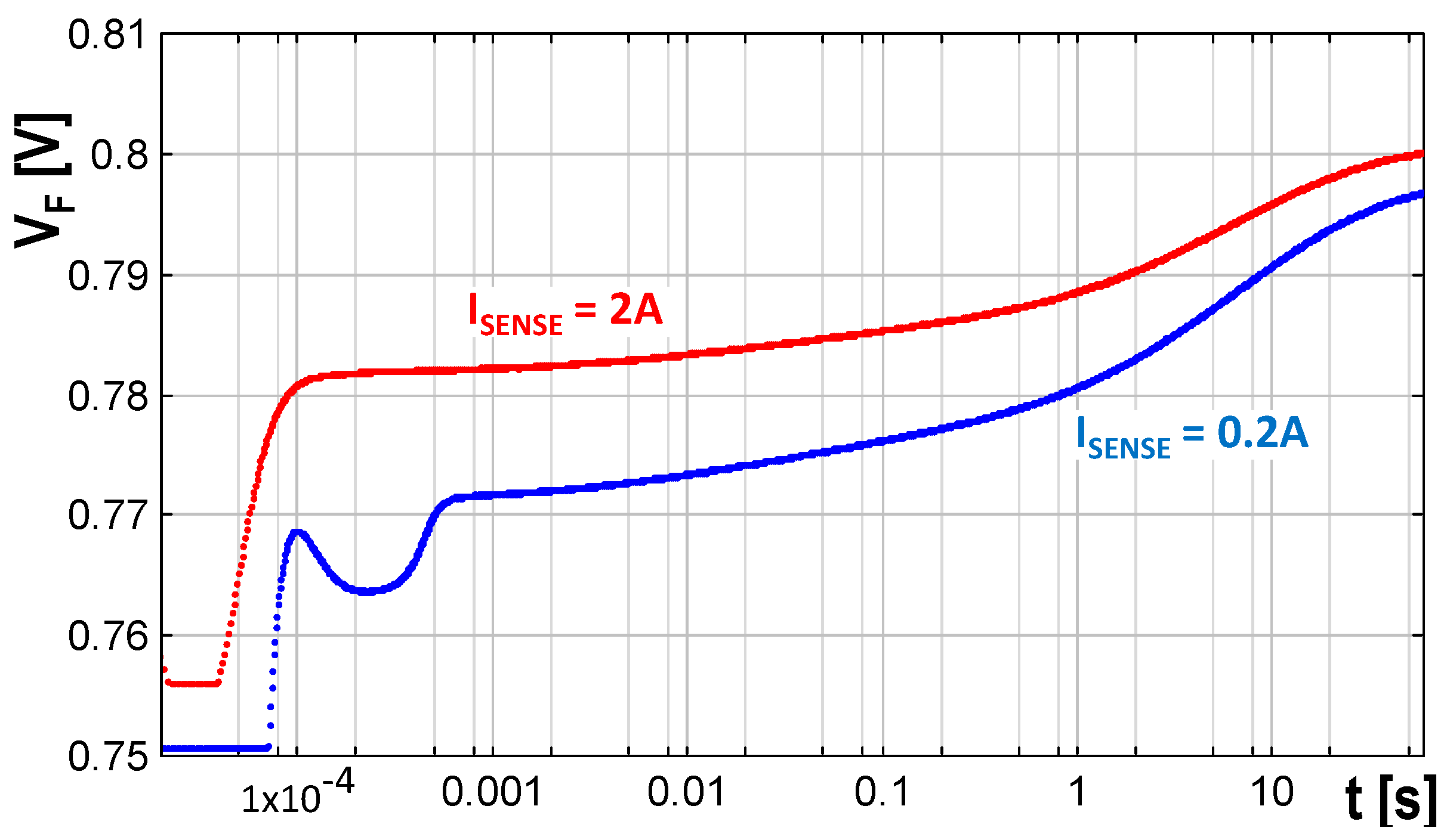
In the scheme of
Figure 1, we recorded cooling transients on one thyristor in the module. The cooling occurred at different sense currents after switching off several amperes of heating current.
Figure 3 shows the recorded transient change of the
VF forward voltage at
ISENSE = 0.2 A and
ISENSE = 2 A sense current levels.
We can observe that as 0.2 A is still near to the hold current threshold of the thyristor, it “attempts” to turn off and recovers around 1 ms only. With ISENSE = 2 A we can expect pure thermally induced transients after 100 μs. The actual “thermally induced” nature of a transient can be verified by comparing a set of measurements at different heating and sensing currents. One can claim that the root cause of the voltage change was the cooling of the device in that time interval, where the curves normalized by the power change coincide (see later Figure 13).
2.3. Transient Test of the Module
With trial measurements similar to the one shown in
Figure 3, we found that a thermal steady state can be reached within one minute on the water cooled cold plate.
Below we illustrate the test and its evaluation on an exemplary measurement at 40 A heating current and 2 A sensing current. A related study with more examples was conducted previously [
10].
An examination on the validity of using other heating and sensing current values will be given below in
Section 3.3.
At these currents we experienced crisp, noise-free thermal transients (shown below in Figure 5).
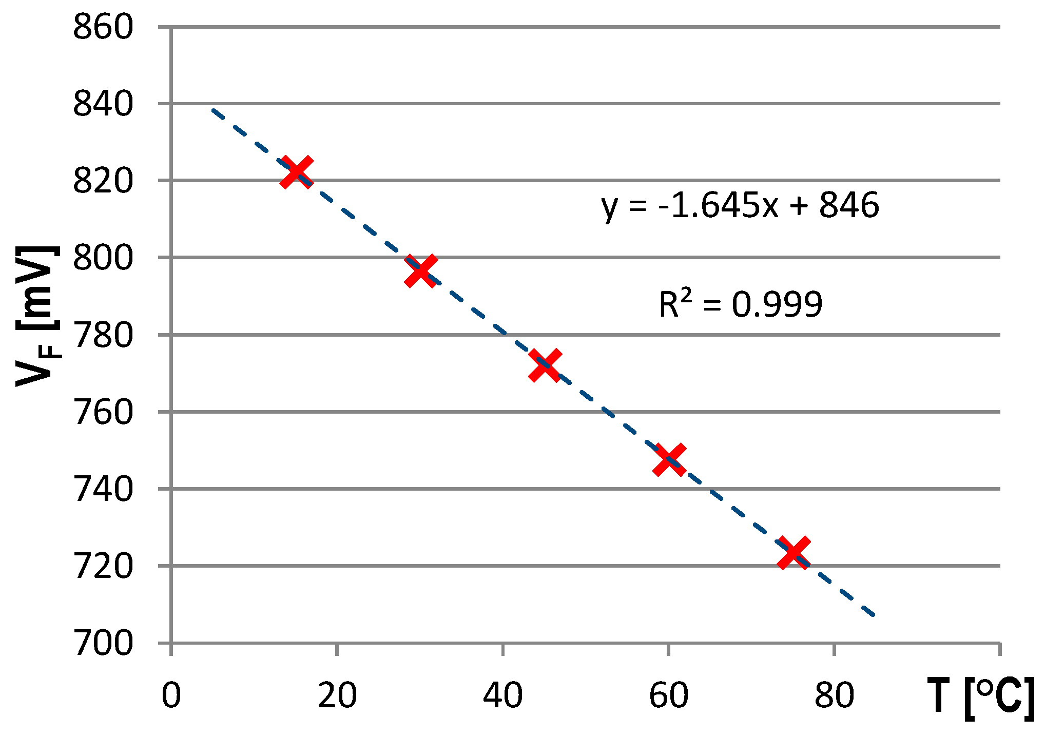
The calibration (
Figure 4) showed that the temperature dependence of the forward voltage is quite linear at the 2 A sensor current, the slope of the plot is
S = –1.645 mV/K. This mapping scales the temperature axis of
Figure 5.
In the testing of devices of extreme die size (processors, for example) or devices made of wide band gap semiconductors, the voltage to temperature mapping is nonlinear. Up to date evaluation software products can store the calibration chart and can calculate the absolute temperature value during a transient from the actual voltage value [
12]. It is important to emphasize that in further sections of the paper we assume linearity of the thermal parameters of the assembly (thermal conductivity, specific heat) but no linearity of the electric behavior or the voltage-temperature mapping is needed.
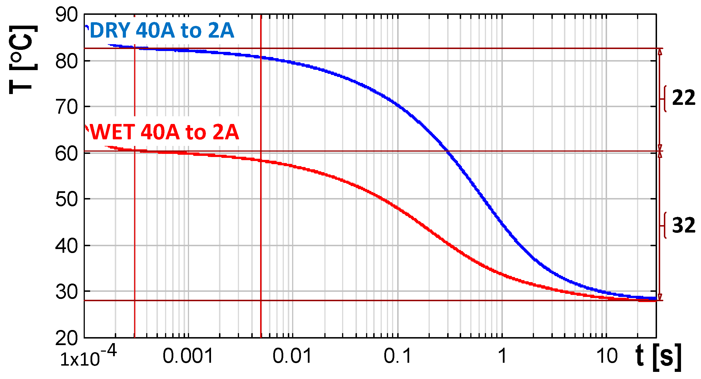
The figure reveals that approximately 54 °C temperature elevation occurs at the “dry cold plate” boundary at 40 A/43.5 W heating (curve DRY 40A to 2A). Using thermal grease the temperature change drops to 32 °C (curve WET 40A to 2A; the figure keys correspond to these boundary conditions in subsequent figures).
An elaborated description of this experiment and its evaluation is given in a previous study [
11].
3. Structure Analysis
3.1. Zth Curves
In
Figure 5 we see many details already. Based on former works we can attribute the temperature change in the millisecond range to heat propagation in the die and through the die-attach, in the second range to the cooling mount, in the minute range to heating of the circulated water, etc. This plot, however, characterizes the heat conducting path only at the given powering.
A more general portrayal of the thermal behavior of an assembly is based on the theory of linear time invariant (LTI) systems. While the electronic devices are strongly non-linear in their electric characteristics, the thermal conductivity and specific heat of the device components and of the measurement environment shows only a minor change in the typical temperature range of use. This means that by shifting the base plate temperature we obtain similar recorded curves and by altering the applied power we obtain similar, proportionally magnified records.
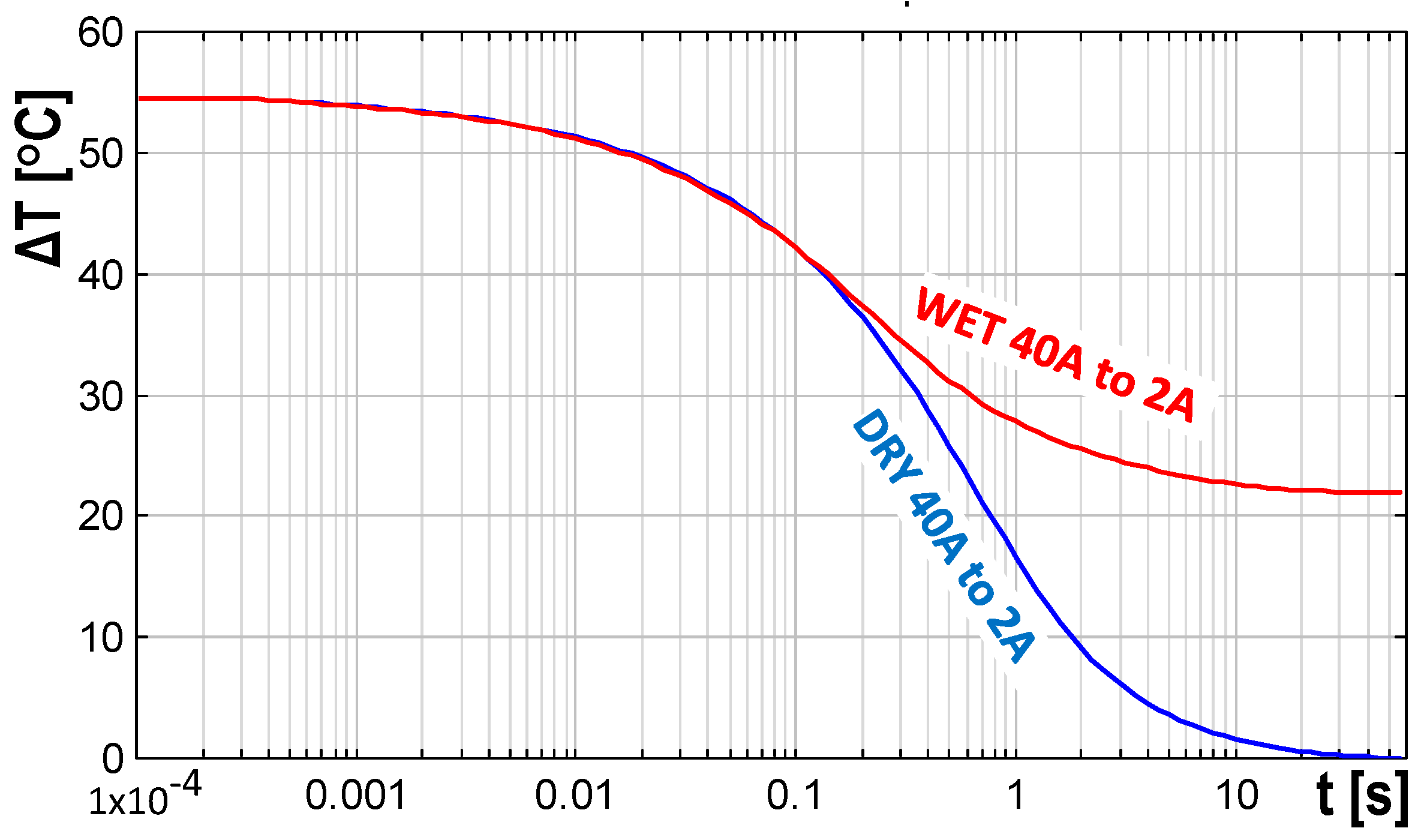
Reducing the cooling curves to temperature
change only and fitting them at their hottest point (
Figure 6), we find that the cooling is not influenced by the actual boundary condition until 0.2 s, and the curves coincide perfectly. This can be explained by stating that until 0.2 s the heat propagates inside the package, and it still did not reach the air/grease thermal interface.
Normalizing the cooling curves with the applied power we obtain the Zth curves. (They are sometimes called “thermal impedance”, but in a strict interpretation an impedance is defined in the frequency domain.) As a fairly accurate temperature transient for any power step can be produced if we multiply the Zth curves by the actual power, this curve is used frequently for the characterization of the thermal behavior.
This concept of proportionality to power is not fully accurate. At increased power level and higher temperature elevation, the cooling mechanisms (turbulent convection, radiation) become more intensive; the real temperature change is lower than the one extrapolated from the multiplied Zth curve. As such, using Zth for temperature estimation remains on the safe side.
A deeper analysis of nonlinear effects is given in another study [
3].
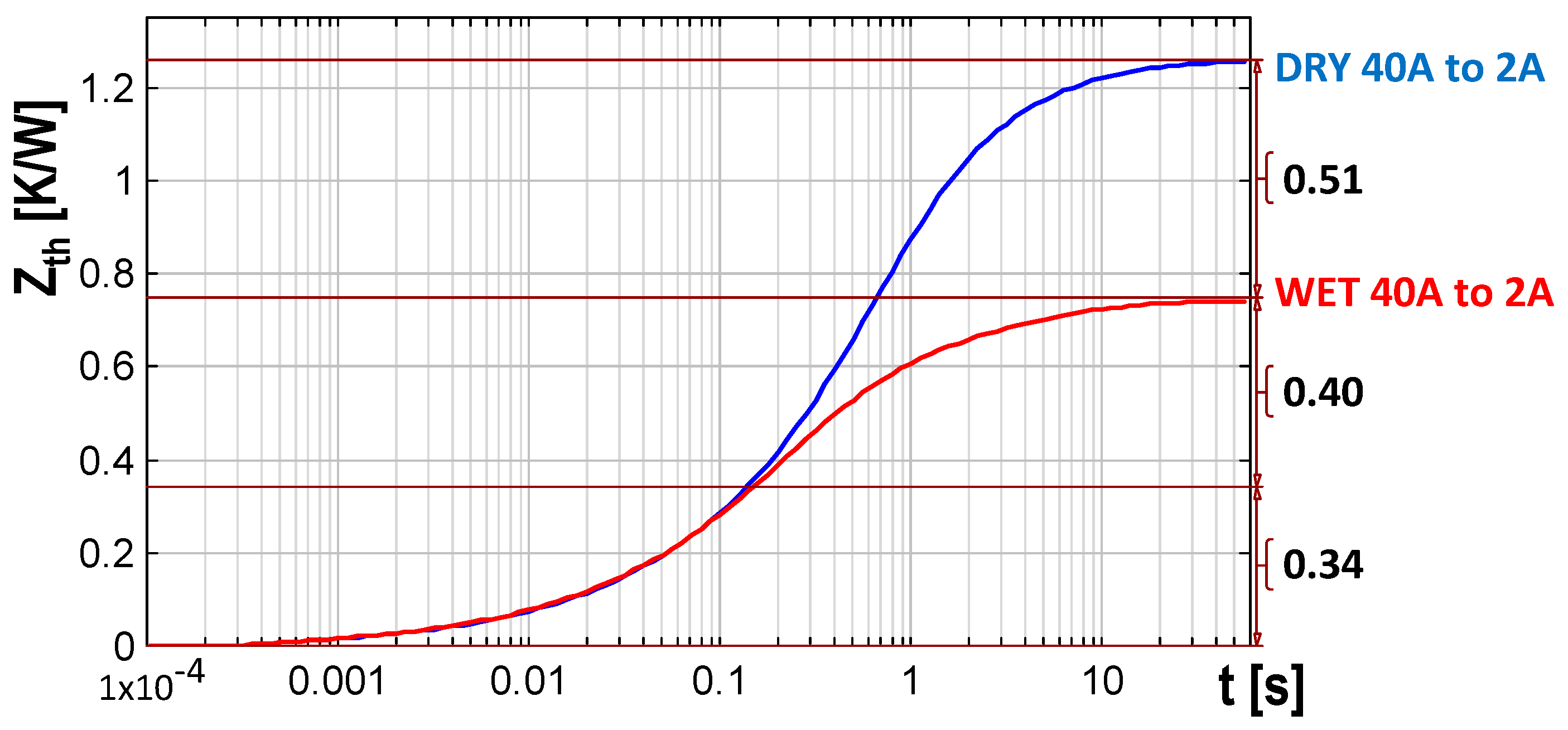
Dividing the curves in
Figure 6 by the corresponding negative power step from
Table 1 (around –44 W), we get
Figure 7.
We can observe in the plot that until approximately 0.2 seconds and 0.34 K/W, the Zth curves coincide because the heat still proceeds in the internal structures of the device. The gradual divergence of the curves indicates that not all trajectories of the heat flow arrive at the same time to the case surface. A way to give a more definite determination of the separation point will be highlighted in the next section.
The arrangement shows 0.74 K/W total thermal resistance with the “wet” and 1.25 K/W with the “dry” thermal interfaces.
3.2. Structure Functions
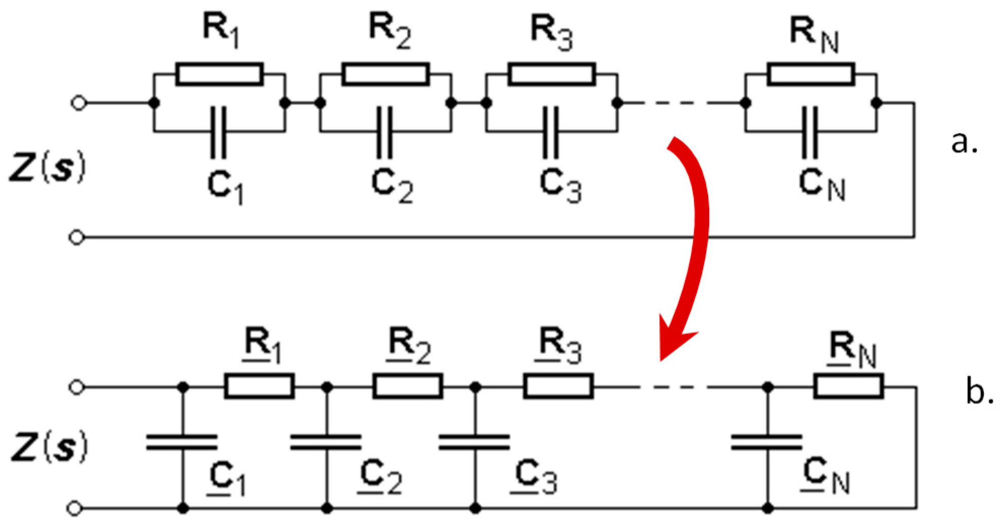
A much more informative representation of the assembly can be derived from the transients, constructing an equivalent RC circuit of thermal resistances and capacitances, producing the same Zth as the assembly, at the same excitation.
Actual thermal systems correspond to a complex three-dimensional RC net. In the case of a single heat source, it can be treated as being excited by
P(
t) power changing in time at a node in the net and terminated by constant temperature at the boundaries. LTI theory claims that such a system behaves in the same way as a reduced set of thermal resistances and capacitances arranged in one of the configurations shown in
Figure 8. (In an analogous electric RC network the
P power applied on the input equals to an
I current and the temperature change in the net corresponds to
V voltage on the nodes.)
If constant
Pon power is switched on at zero time (step function), a single series RC element in
Figure 8a produces an exponential growth after switching on the power (current), adding
T(
t) =
Pon R⋅(1 –
e – t/τ) temperature (voltage) term to the chain response. The
Ri magnitude denotes the thermal resistance of the
ith fragment; τ
i =
Ri⋅ Ci is a
time constant, where
Ci is the thermal capacitance. Accordingly, at the input (in this case at the junction) we get a
sum of exponential functions,
The Network Identification by Deconvolution (NID) method [
1,
6] provides a systematic methodology to produce several hundred RC stages, resulting in a highly accurate approximation of the original
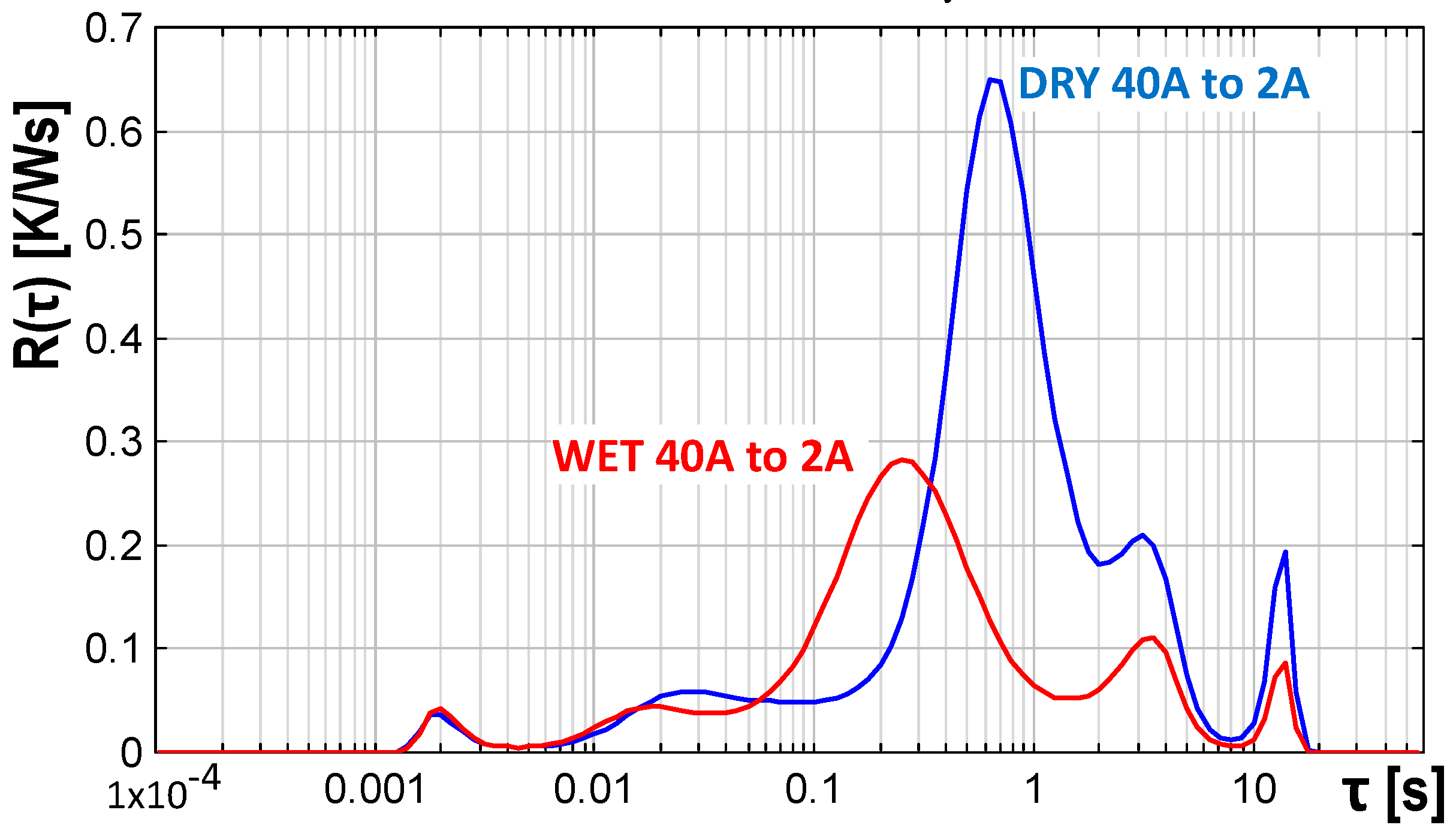
Zth curve. The time constants distilled from the curves of
Figure 7 are shown graphically as an
R(
τ) time constant spectrum in
Figure 9.
The information in time constant spectra is hard to interpret. A more usable representation of the system can be gained converting the RC stages of
Figure 8a into an equivalent RC ladder of
Figure 8b, as demonstrated in previous studies [
1,
6,
13]. Instead of providing hundreds of R and C values in tabular format we can construct a graphic representation, the
structure function.
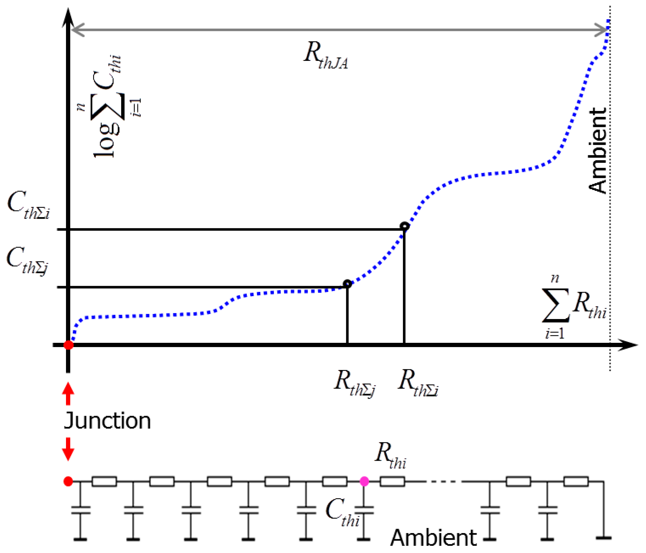
In this chart (
Figure 10) we sum up the thermal resistances in the ladder, starting from the heat source (junction) along the x-axis and the thermal capacitances along the y-axis. (The Σ sign in the axis keys refers to the cumulative nature of the function, and to the fact that ladder elements are added up along the axes.)
Thermal capacitance is proportional to the mass and volume of a material layer through its specific heat and density. Low gradient sections in the chart mean that a small amount of material having low capacitance causes large change in the thermal resistance. These regions have low thermal conductivity or small cross-sectional area. Steep sections correspond to material regions of high thermal conductivity or large cross-sectional area, as even a large bulk of material corresponding to high thermal capacitance is of low thermal resistance only. Sudden breaks of the slope belong to material or geometry changes. Thus, thermal resistance and capacitance values, geometrical dimensions, heat transfer coefficients, and material parameters can be directly read on structure functions.
3.3. Examination of the Magnitudes for Valid Heating and Sensing Currents
The widespread misconceptions in the thermal management community regarding the required current levels during transient testing can be summarized in the following two points:
The heating current has to be high enough to reach at least 30 °C to 50 °C temperature elevation, otherwise the measurement will be of limited accuracy;
The sensing current has to be kept low in order to avoid the “self-heating” of the die in the cooling phase.
The first postulation is simply projected from the poor specification of old thermal transient testers. Current test equipment has 10 μV voltage and 0.01 centigrade temperature resolution, which enables it to record a temperature swipe of 5 or 10 centigrade at low noise and full accuracy.
Regarding the second point, in the previous measurements we captured the temperature of a single point only, on a single data acquisition channel of the test equipment.
This technique is compliant with the present thermal transient testing standards [
6] and is advantageous in many ways. First of all, all channel offset and gain errors of the equipment are cancelled-out during the calibration process of
Section 2.3, so the only source of error can be the inaccuracy in the thermostat temperature. On the other hand, as the change of the
Rth thermal resistance is negligible in the span of the measurement, a higher sensor current just adds a constant (small) temperature shift to the actual transient, not influencing the calculations based on the
change of the temperature.
The source of the misconception regarding the allowed sensing current is an incorrect interpretation of the standards [
4,
5]. If the temperature difference at the junction is derived from the temperature of two separate points
in space, e.g., from the voltage of the hot junction and some data from a different temperature sensor at a distant point, and moreover if these are measured on different tester channels, then:
Sudden change of the Rth thermal resistance can occur in special cases, e.g., at phase change in the thermal interface materials. This may undermine the accuracy of the one-point measurement, but then the methods based on temperature measurements at distant points are equally invalid.
As an example, we can calculate the extent of the measurement error in the test presented in
Section 2. The equipment recorded
VF1 = 1.1 V forward voltage on the “hot” device at
IHEAT = 40 A heating current, with
ISENSE = 2 A added after a longer stabilization period. This resulted in
P1 = (
IHEAT +
ISENSE)
⋅ VF1 = 46.2 W power on the device just before switching off the heating.
After switching off the heating, the device forward voltage at ISENSE = 2 A started at VF2 = 0.75 V. Then, in 60 seconds this forward voltage grew by approximately 50 mV, to VF∞ = 0.8 V. Just after switching off there was P2 = ISENSE ⋅ VF2 = 1.5 W power on the device. The power step is P1 – P2 = 44.7 W.
This calculation differs slightly from the actual measured power step in
Table 1 due to rounding.
The only real source of inaccuracy that has an effect other than a constant shift in the junction temperature is the slow change of power during cooling, at the end of which the power grows to P∞ = ISENSE ⋅ VF∞ = 1.6 W, and the error in powering during the full cooling period is P∞ – P2 = 0.1W; compared to the power step this is 0.224%.
Table 2 summarizes the device temperature and powering error based on measured and calculated voltages at fixed heating and different sensing currents. The voltages and temperatures of row
a corresponding to 2 A sensing current are taken from the actual measurement. Row
b and
c contain
VF (
IF) forward voltage data calculated from the exponential characteristics of a pn junction at low current (Shockley equation), which claims that an 1:10 shrink of a (low) forward current causes 60 mV voltage shrinkage at room temperature. Temperatures in rows
b and
c are calculated from the
Rth thermal resistance of the assembly and the
S voltage-to-temperature sensitivity of the device, as identified in
Section 2 above.
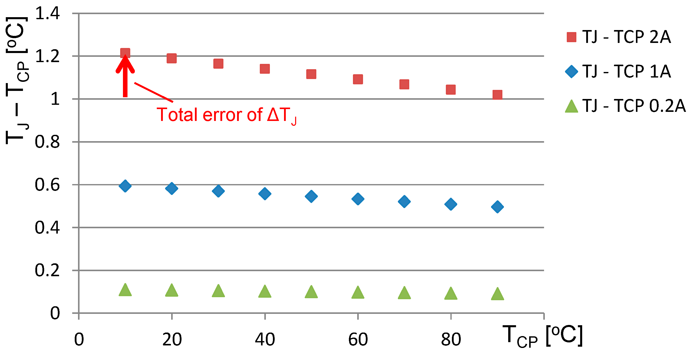
Figure 11 below demonstrates the absolute error of the calibration in the 10 °C to 90 °C temperature range, at 2 A, 1 A, and 0.2 A sense currents. The maximum error over 80 °C temperature change is 0.2 °C.
In the case when an exact
TJ junction temperature has to be achieved at high heating current, a corrective step in the cold plate temperature regulation can be performed to reach precisely the target temperature. This occurs at the combined thermal and radiometric and photometric measurements of high-power LED devices, where the optical characterization takes place in the thermal steady state at accurate junction temperature before initiating the cooling. The
Rth thermal resistance of the assembly can be determined for this correction by transient measurements before starting the actual test [
14].
4. Case Studies
Below we present a series of examples where changes in the whole heat conducting path can be identified with the help of structure functions in a different manner.
4.1. Structure Functions of the Solid State Relay Module
Converting the
Zth curves of
Figure 7 to structure functions we gain
Figure 12. In this figure and in other figures below, the steep sections (high change of thermal capacitance along small thermal resistance) belong to silicon or metal layers in a laminate structure, and flat sections (low change of thermal capacitance along large thermal resistance) are thermal interface materials (TIM). Each dot on the curve represents a thermal resistance–thermal capacitance pair.
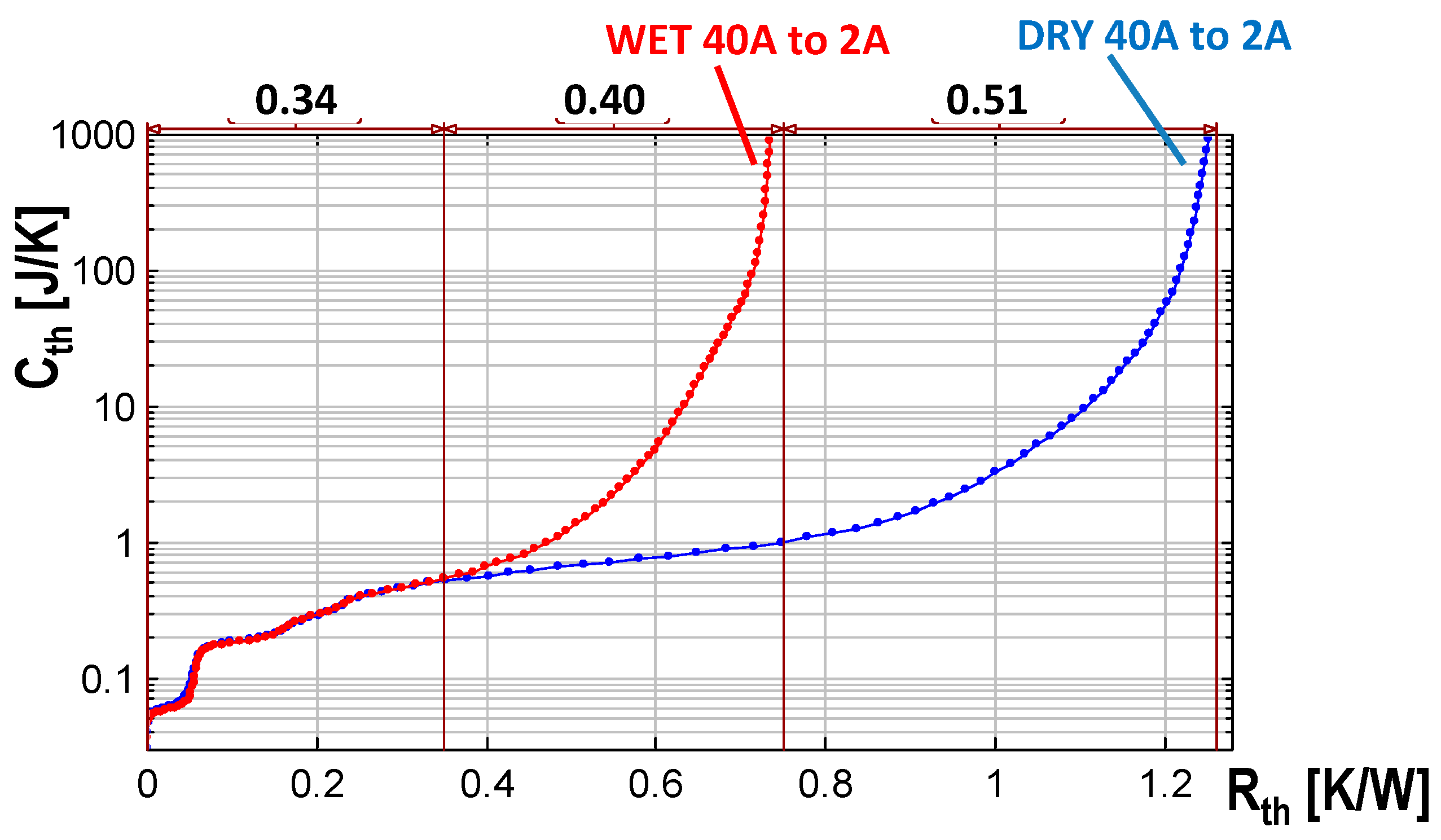
Up to 0.34 K/W the steps in the function indicate the sandwich-like internal structural details, such as die, solder, and ceramics (DBC). The physical dimensions, volumes, and distances can be read in the chart if some material parameters are known, or in other cases, the thermal conductivity and specific heat can be determined if the geometry is known. After the junction to case separation point, we see the heat spreading in the grease and the cold plate.
Thermal capacitance values above Cth = 1000 J/K are not shown in the figure. Already 100 J/K thermal capacitance would correspond to 4000 mm3 volume of the aluminum cold plate used in the measurement arrangement, 1000 J/K would correspond to 40000 mm3 of aluminum. This volume of aluminum is not present in the proximity of the device, so this Cth range belongs rather to the capacitance of the water flow in the plate. In this way the structure function portion depicting higher capacitance is not informative regarding the device under test.
The air gap on dry surfaces adds 0.51 K/W to the junction to ambient total thermal resistance.
It has to be mentioned that the structure function analysis is not a “black box” technique. There are three ways to assign actual assembly components to sections in the structure function. These are:
The manufacturer of the device may know all internal geometries and material parameters. In such a way a “synthetic” structure function can be built up, for example, superposing slices of material with given thermal resistance and capacitance in a spreadsheet tool, and comparing the measured structure functions to it;
An approximate model can be built up in a finite element or a finite difference simulation tool, such as [
15]. Thermal transients can be simulated in the tool and structure functions can be composed of those. Geometry and material parameters can be tuned until the simulated and measured structure functions match;
Measured structure functions can be compared to an already identified “golden device”. This technique is advantageous in production control.
In the case of simulation, the environment farther from the device does not need detailed modeling, as it is often replaced by a surface with a constant heat transfer coefficient (HTC) applied.
Air or liquid cooling is nearly proportional to the area where it is applied.
In the actual measurement the cooling occurs on the copper coated ceramic base plate of the module. The physical samples and also the module geometry in the data sheet indicate approximately 20 mm × 40 mm (0.0008 m2) as the effective contact area.
From the partial thermal resistance values after the divergence point in
Figure 12 we can estimate the quality of the heat sink. We can calculate HTC = 1/(0.4 K/W ⋅ 0.0008 m
2) = 3125 W/m
2K for the “wet” surface and HTC = 1/[(0.4 K/W + 0.51 K/W)⋅ 0.0008 m
2]= 1373 W/m
2K on the “dry” surface. These values are near to the ones published in the literature.
4.2. Measurement of a Large Digital Signal Processor
It is a really challenging task to measure the thermal performance of large processor, memory, or gate array circuits. Their size can be of several cm2, the die is thin, and the package is optimized for low thermal resistance.
In this example we present the typical obstacles experienced in the measurement of processor devices. These are typically powered and measured in a thermal test on their substrate diode, which covers the whole silicon surface and can be reached by reversing the supply and ground of the circuit.
These devices have separate supplies for their core, internal storage, and peripheries. The different functional parts in the chip and the isolation among them form complex pnpn structures. These parts share different current bias levels in different proportions and tend to inject charge into each other in a thyristor-like manner.
In the actual test a large, experimental digital signal processor (DSP) circuit was measured. The die of the circuit was 20 mm × 20 mm size and was encapsulated in a ball grid array (BGA) package with soldered die-attach, ensuring low thermal resistance.
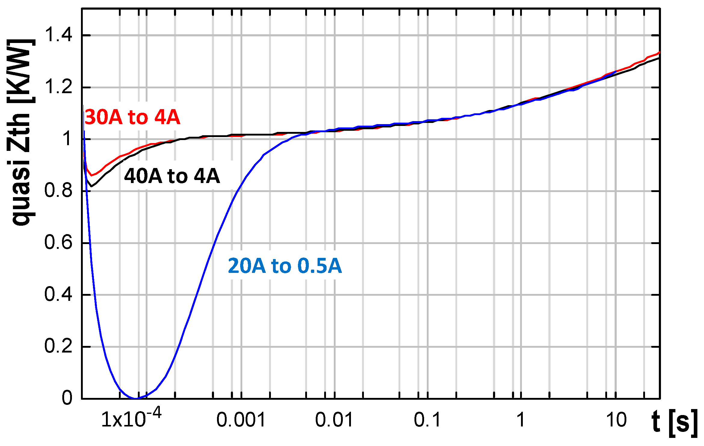
To obtain a valid thermal signal we had to carry out experiments in a wide
ISENSE sensing current range starting from milliamperes up to several amperes. To arbitrate the quality of the result we normalized the measured transients with the applied power, but without correcting the initial electric transient of the signal. In this way we produced “quasi
Zth “curves, having no thermal nature in their initial portion (
Figure 13).
We found that even in the sensing current range of 0.5 A to 2 A, a time variant redistribution of charge occurs until several milliseconds. At 4 A sensor current we experienced a clean thermal signal from 200 μs onwards.
This measurement also supported the general observation that the longest time interval where a transient of true thermally induced nature can be taken can be achieved with a high sensing current and low heating current. This approach minimizes the electric effects at the current level change, and does not diminish the accuracy of the measurement, as proved in
Section 3.3.
4.3. Die-Attach Analysis
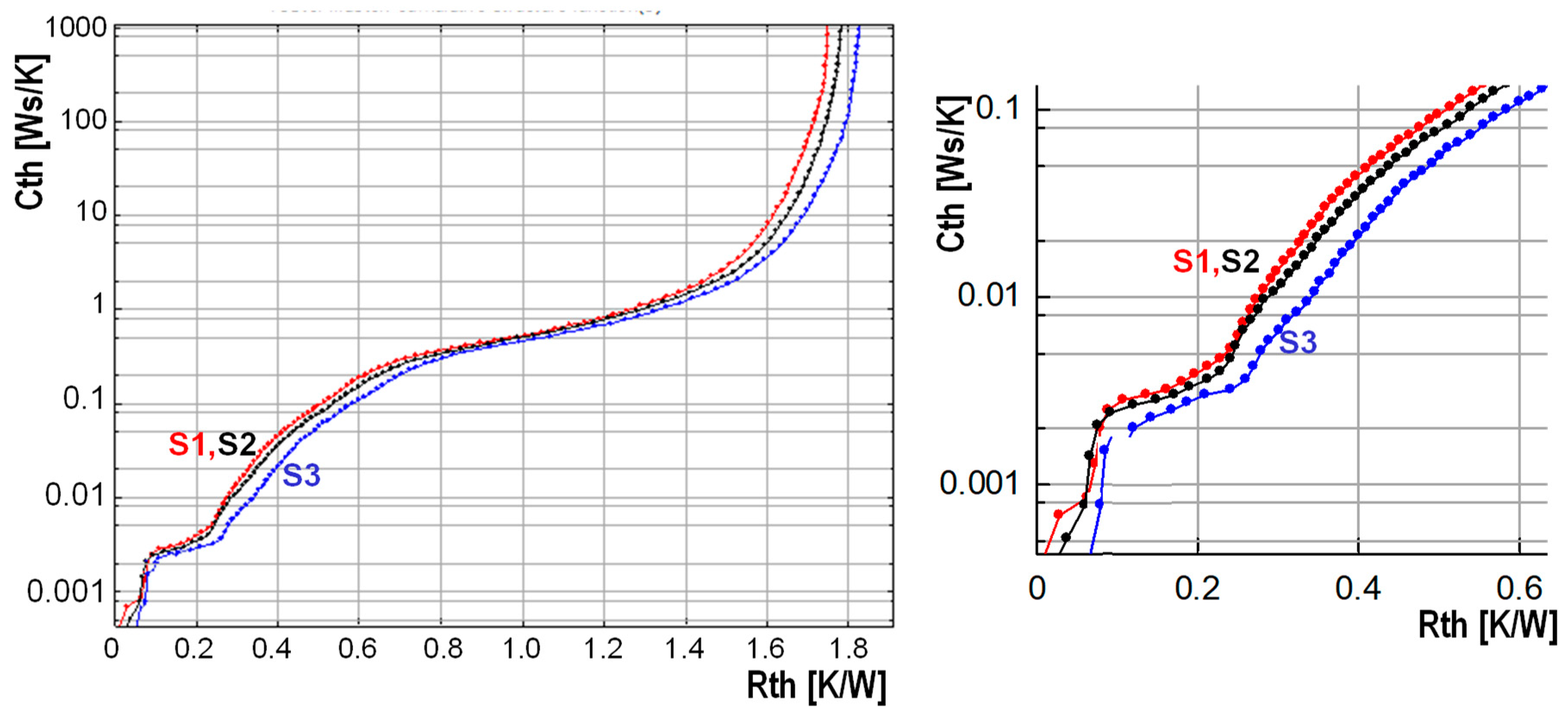
In this study we compare three MOSFET samples (S1, S2, and S3) from the same manufacturing batch. Measuring their structure functions on a cold plate we gained
Figure 14.
Sectioning the samples after the measurement revealed that the volume of the silicon die is approximately 2 mm
3, having an effective thermal capacitance of approximately 3.2 mJ/K, calculated from the specific heat of the material. We find this
Cth value around 0.1 K/W in
Figure 14. The structure function is very flat until 0.25 K/W, i.e., in this section there is a material of low thermal conductance, in our case a soldered die-attach with less than 20% of the silicon’s thermal conductivity.
The end of the die-attach region is clearly indicated by a sharp increase of the structure function at around 0.2 K/W. Differences between the samples develop in the die-attach region and all curves run parallel afterwards.
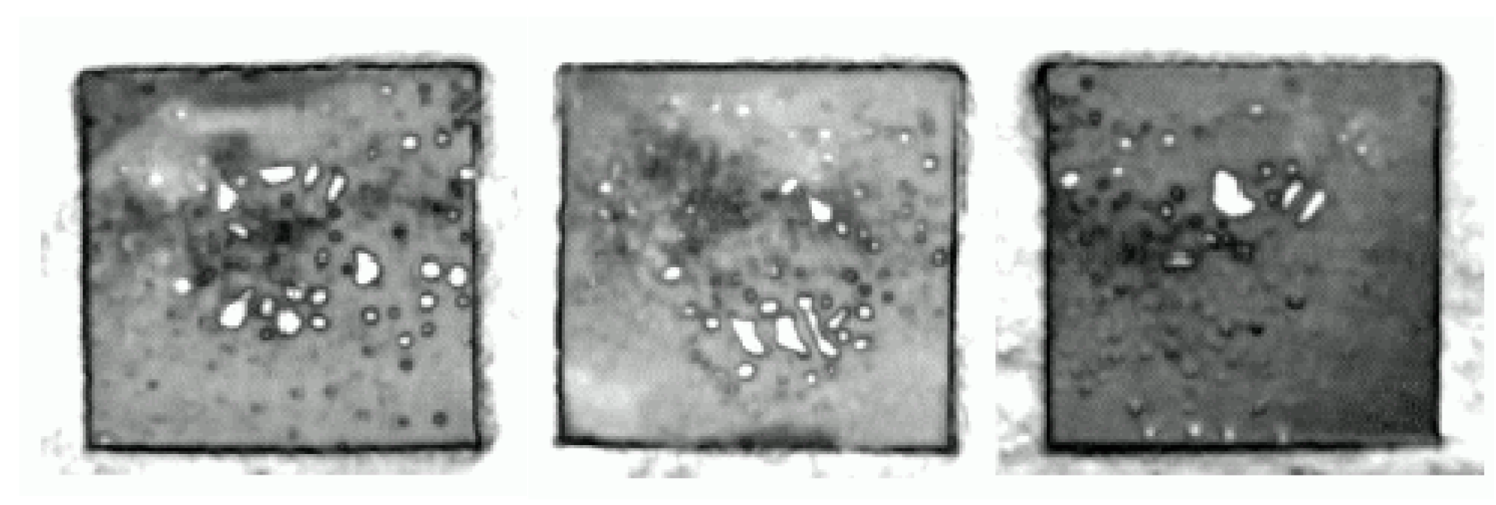
We verified by scanning acoustic microscopy (SAM) pictures as shown in
Figure 15 that S3 (darker in
Figure 15) has a thicker solder layer than the other two. The white spots correspond to solder voids, but they have minor importance regarding the thermal resistance.
As the die-attach is the most critical part of any electronics assembly from a reliability point of view, thermal transient testing and structure function analysis are used most frequently for die-attach testing.
4.4. Design of the Package or Module Base Plate
In this study we show a measurement example with identical dice encapsulated in packages of different base plate thickness.
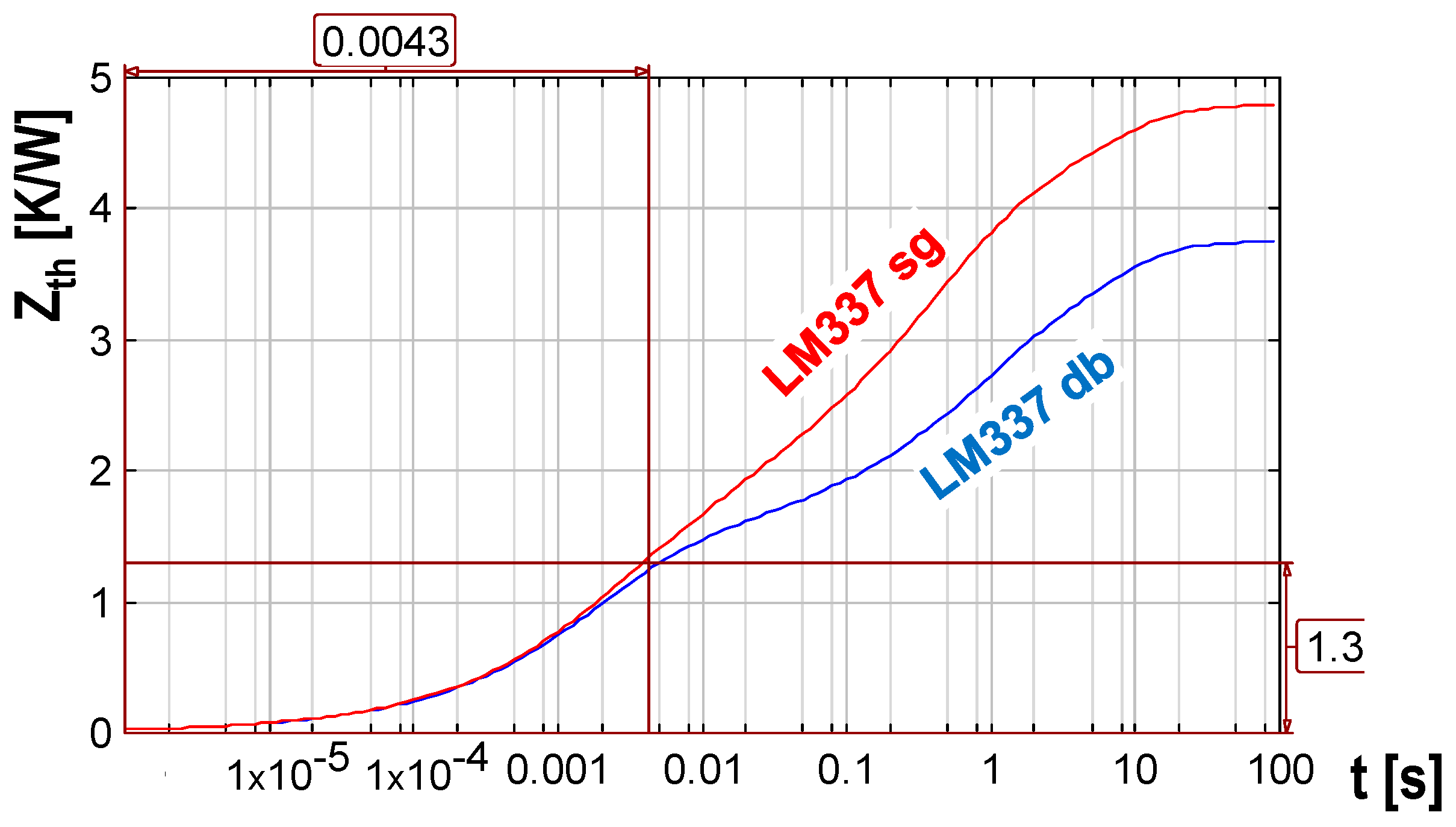
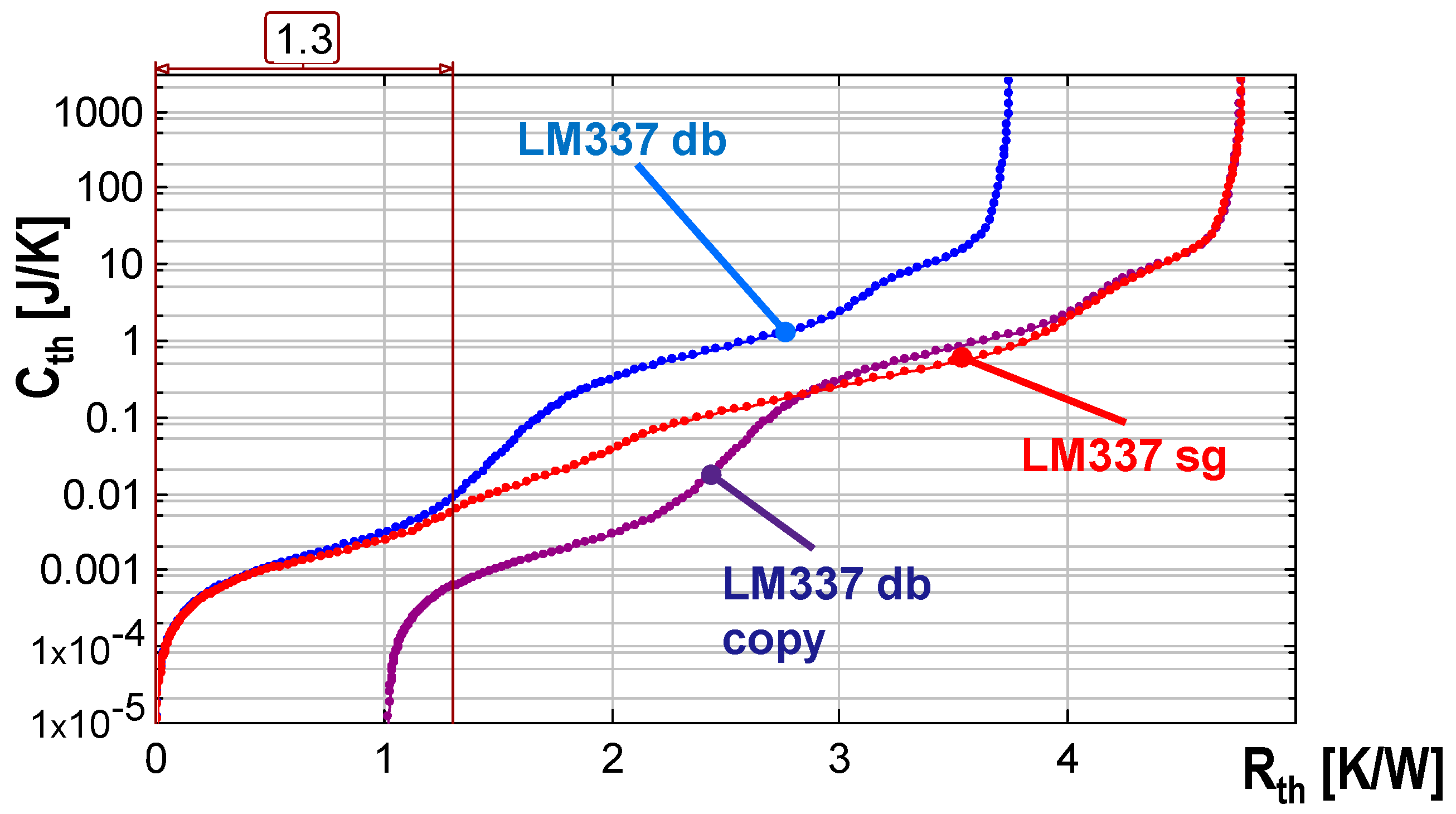
The standard LM337 voltage stabilizer exists in TO-220 packages with single gauge (d = 0.51 mm) and double gauge (d = 1.3 mm) tab thickness construction (
Figure 16). It is hard to predict whether a thinner heat spreader performs better or worse if the device is mounted on a heat sink.
Figure 17 already shows that the single gauge solution (LM337 single curve) is of slightly worse thermal performance; however, the reasons remain unclear.
Figure 18 demonstrates that up to 1.3 K/W the heat propagates internally in the die and die-attach. The divergence point of the
Zth curves indicates that at 4.3 ms the trajectories reach the inner surface of the copper tab. We can observe the quick elevation of the thermal capacitance in the double gauge tab, corresponding to a broad heat spreading cone in which the heat crosses the die to tab interface, resulting in a total of 3.8 K/W junction to ambient thermal resistance, as opposed to 4.8 K/W for the single gauge.
Making a copy of the double gauge structure function and shifting it to the ambient end in
Figure 18, we can observe that between 4 K/W and 4.8 K/W the curves coincide, as in both cases this final portion of the structure functions already belongs to the measurement environment. The partial resistance of 0.8 K/W belonging to the cold plate can be determined.
4.5. Discovering Run-in and Curing Effects in the TIM Layer at Power Cycling
Let us now turn back to our original assembly of
Section 2. The standard junction to case thermal resistance measurement (
Section 2 and
Section 3) already marked out the expected junction to ambient thermal resistance variation with “good” and “poor” thermal interface quality.
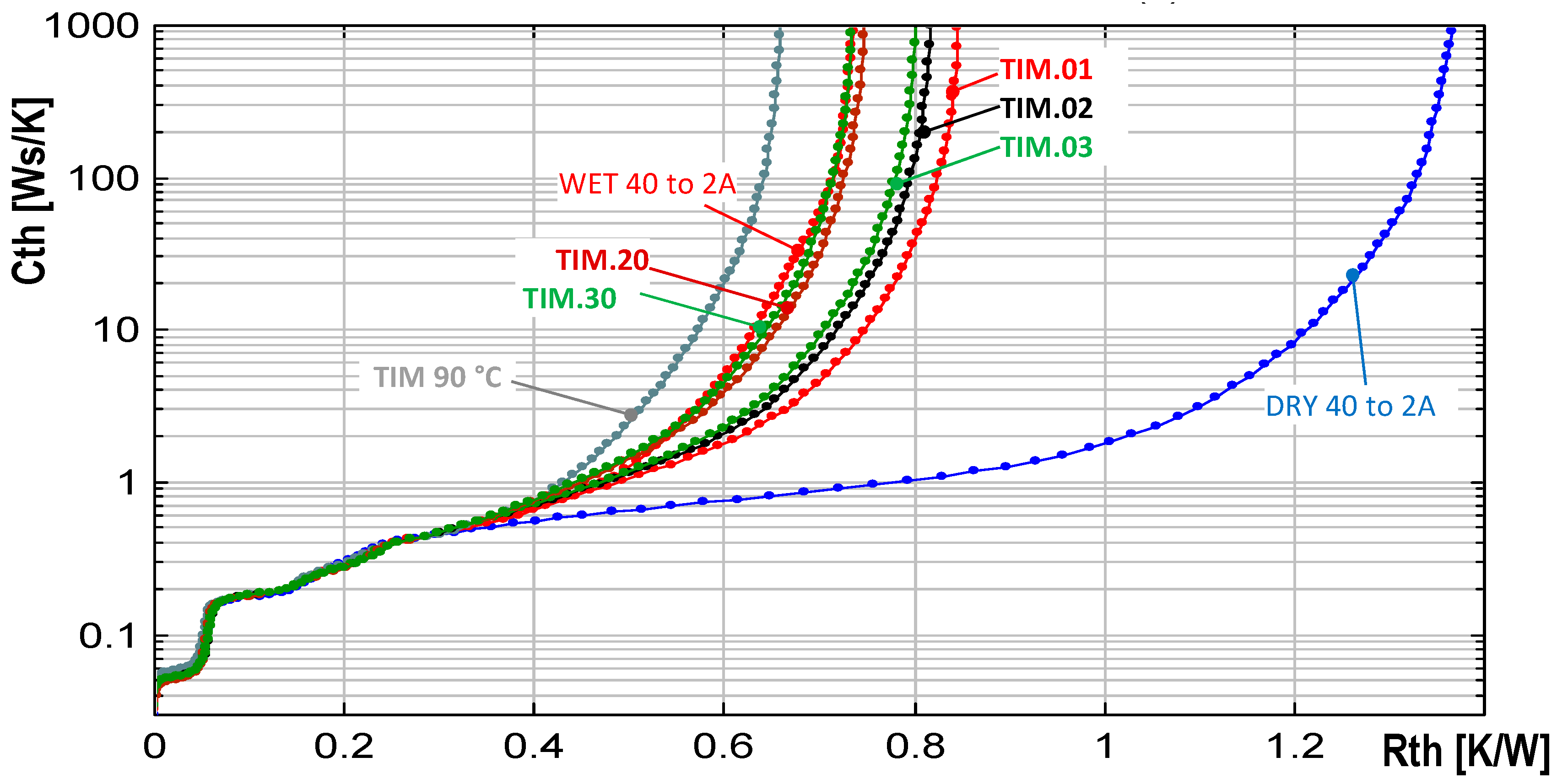
Applying a soft thermal paste on the module base we experience a significant improvement in the thermal behavior compared to the “dry” case. With repeated 44 W power pulses of 60 s length, we see a continuous improvement (run-in) of the TIM layer. The curves from TIM.01 to TIM.30 (here the last two numbers give the cycle numbers) show the thinning of the paste due to temperature and pressure.
After 20 cycles the layer stabilizes and we reach the “wetted by thermal grease” boundary (
Figure 19). Similar cases are discussed in detail in previous studies [
16,
17].
A further improvement could be reached by curing the soft thermal paste at a higher temperature. The module was fixed for 24 hours on a plate kept at 90 °C, with its screws pulled at the 0.9 Nm torque proposed in its data sheet. The paste becomes runny and thin at this temperature and pressure, and fills the rough microstructures of both surfaces. The improvement can be well seen in
Figure 19 (TIM 90 °C curve).
At this point, we have to define the expected power range that has to be applied during the test. Having a sufficiently sensitive thermal tester (as in the reference [
12]), we can see the structural elements in the assembly already at a power level that results in around 4 °C temperature elevation on the die. However, for studying changes within the TIM, especially phase change effects, a real application power level is needed. For accelerated reliability testing, a higher-than-nominal power has to be applied [
16,
18].
This result emphasizes the importance of proper initial handling of TIM layers in critical applications. A well-designed priming power sequence or previous curing of the assembly at higher temperature can prevent early failure of a device due to overheating when first switched on.
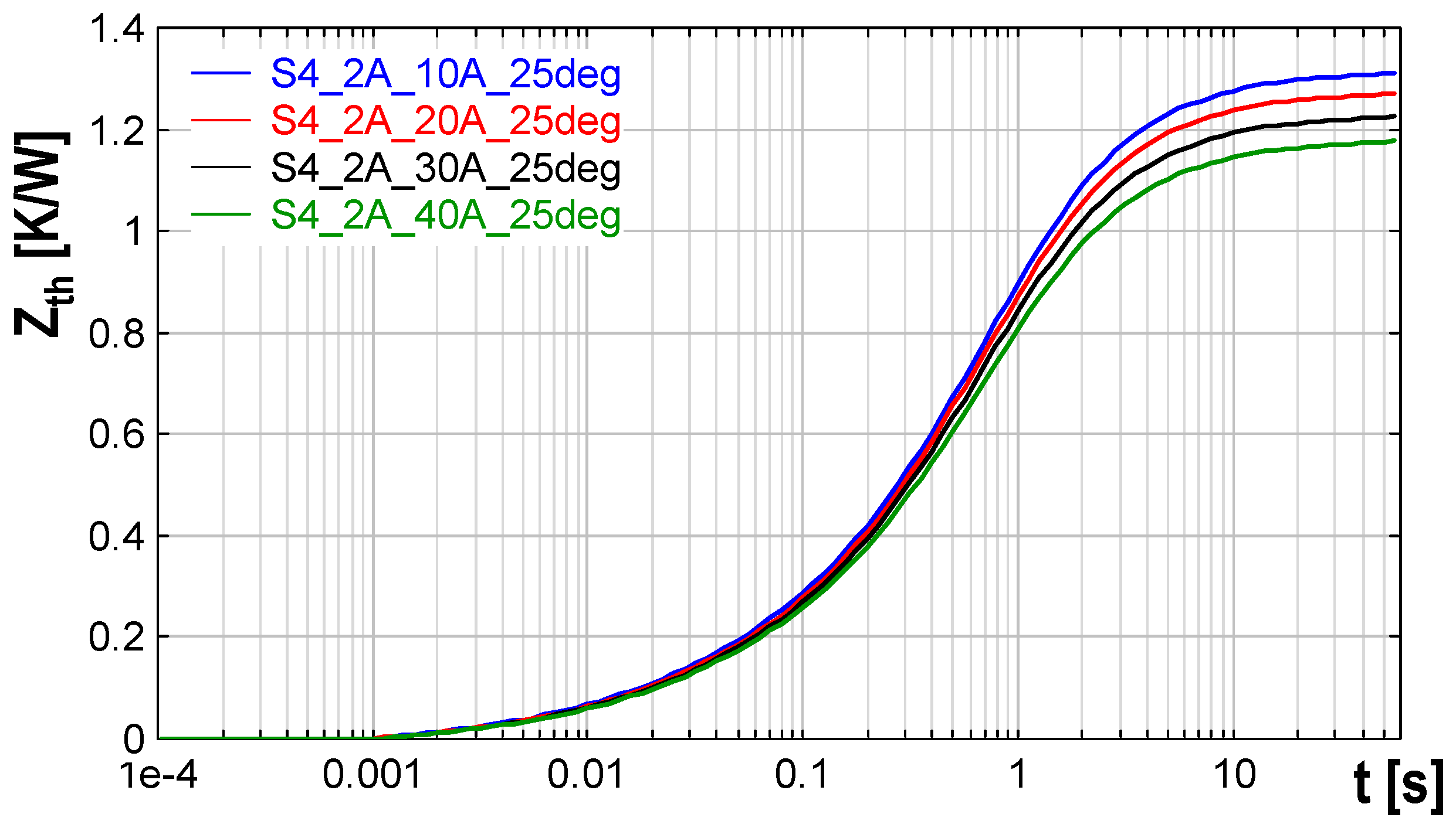
4.6. Testing of Power Modules at Different Heating Currents
We are accustomed to the experience that in the case of discrete power devices, the
Zth curves fit perfectly at all power levels, because the internal wiring is optimized for low voltage drop, resulting in low power loss on the wires. An equally good low power loss characterizes the BGA packaged devices, similar to the one presented in
Section 4.2.
At power switching modules the internal wiring is more intricate and some compromises cannot be avoided. For this reason we typically see a shrinking and growing “accordion” effect in the
Zth curves (
Figure 20) and also in structure functions.
In
Table 1 we summarized the steady state power on the solid state relay of
Section 2 when heated by different currents.
Figure 20 demonstrates the
Zth curves recorded at 10 A to 40A heating current and at 25 °C cold plate temperature.
During the cooling we record the correct die temperature. When composing
Zth curves or structure functions, we divide by the power which is measured across the whole module, including the portion dissipated in the internal wiring. Supposing that we can neglect this power component at 10 A current,
Figure 20 indicates that at 40 A, already 13% of the heating occurs away from the die.
With an appropriate correction factor we can fit the Zth curves again. This factor helps estimation of the actual load on the internal wiring. A scheme of the internal wiring is hinted in Figure 27, for example.
In future test standards it has to be contemplated how appropriate correction factors can be introduced.
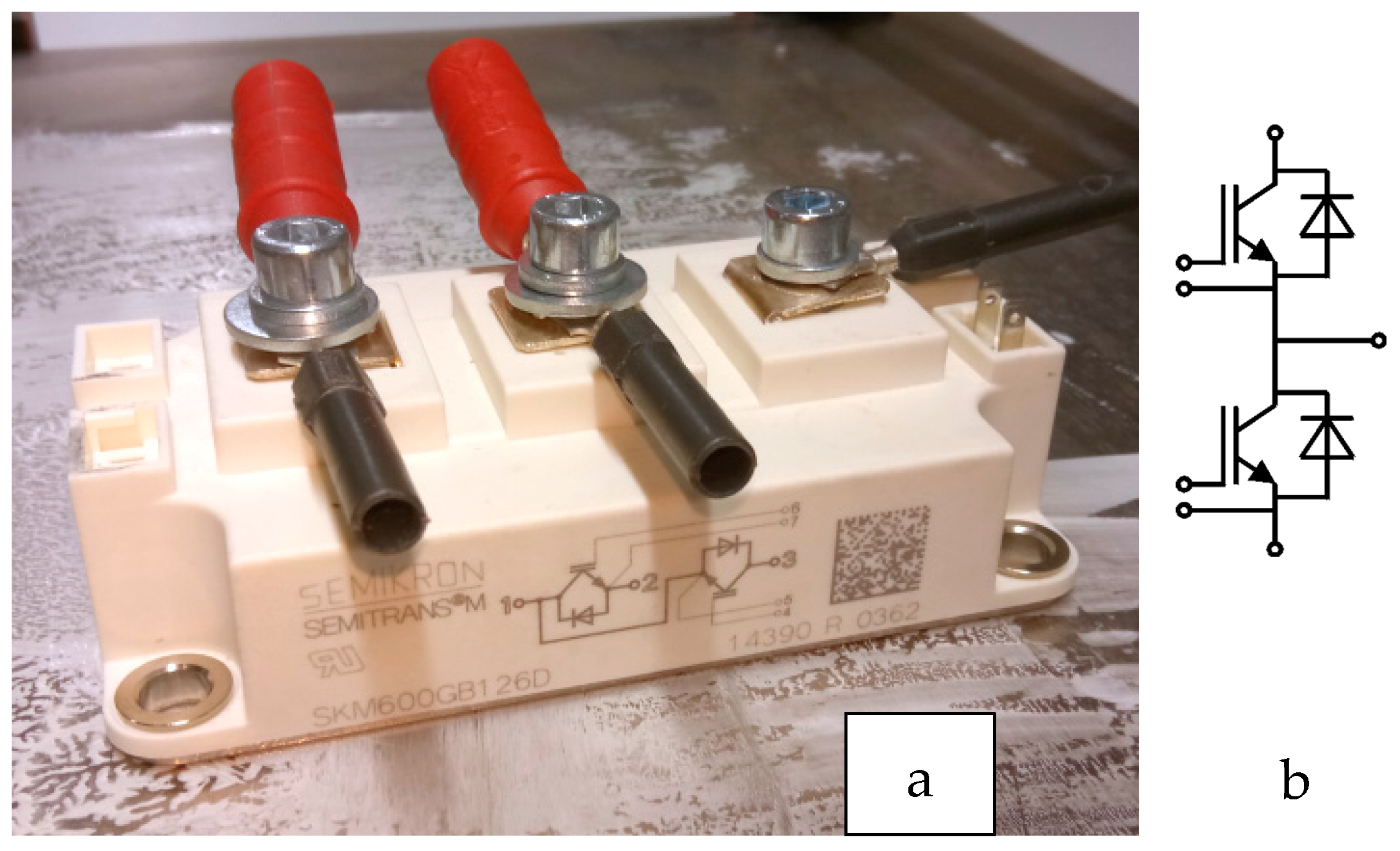
4.7. Heat Transfer in Modules between Dice
We have measured a number of power switching modules and studied the heat transfer from one die to its neighbors. Now, we present measurement results on a typical half bridge module, SKM600GB126D, built of two insulated gate bipolar transistors (IGBT).
This module was also mounted on a water-cooled cold plate (
Figure 21a), with both “dry” and “wet” surface qualities. As there are two IGBTs and two reverse clamping diodes in the module (
Figure 21b), a number of self-heating and transfer-heating configurations can be measured. Now, we limit the test to examining the cross-coupling of the IGBTs.
Applying a high enough V
GE voltage on the gate, the IGBT exhibits diode-like “saturation” characteristics between its collector and emitter. A single device can be well measured in saturation mode, as suggested in
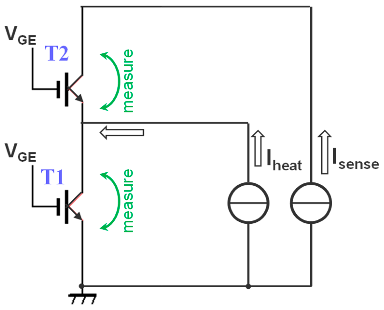
Figure 22. Self- and transfer-heating can be measured simultaneously, as suggested in
Figure 23, maintaining a sensor current on both devices T1 and T2, but heating only T1.
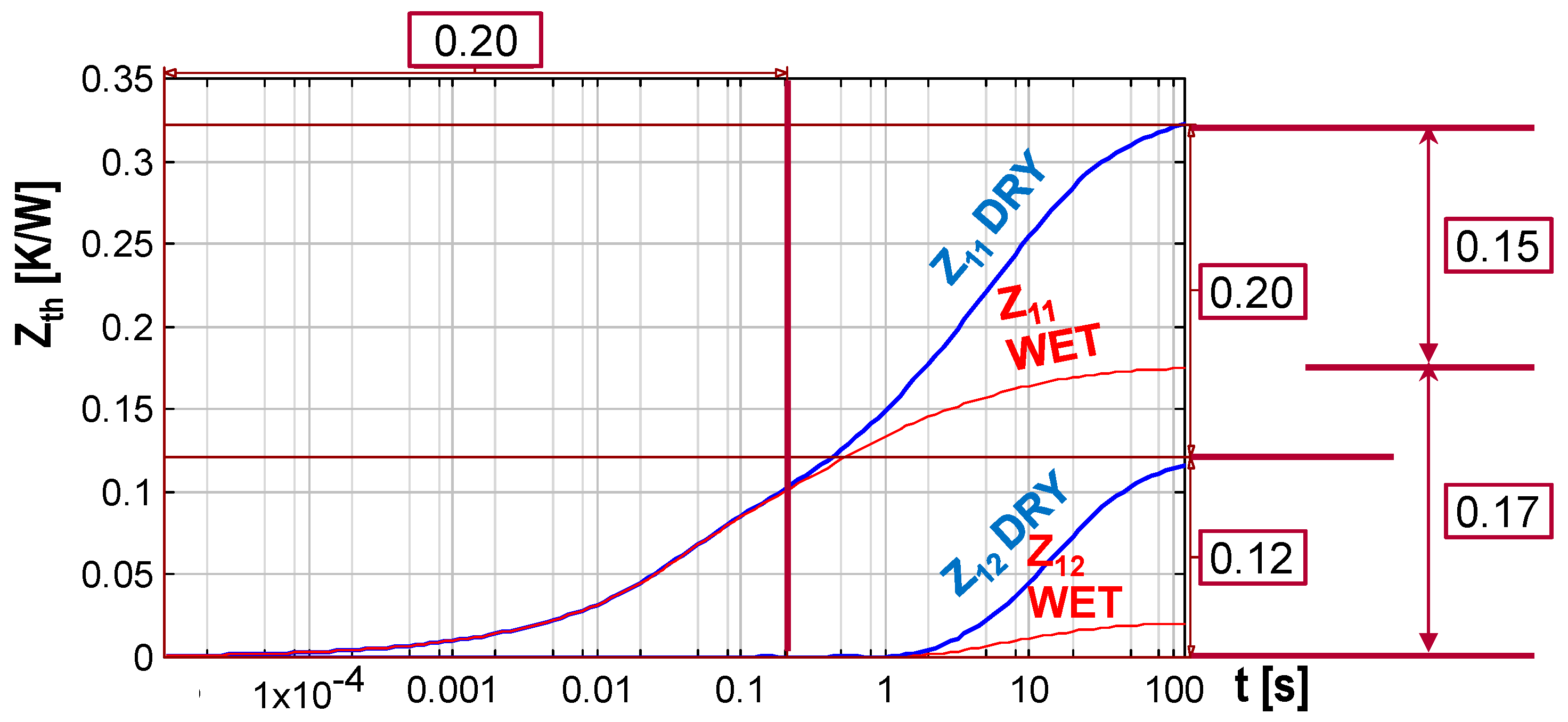
The obtained
Zth curves shown in
Figure 24, namely,
Z11 representing the self-heating and
Z12 corresponding to the heat transfer from T1 to T2, reveal that the runtime between the two IGBT dice is slightly more than one second, here
Z12 starts to elevate.
After 100 s the temperature stabilizes, Z11 reaches the R11 junction to ambient “self” thermal resistance, and Z12 reaches the R12 ”transfer” thermal resistance.
The blue (thicker) Zth curves belonging to the dry cold plate boundary indicate a junction to ambient thermal resistance of R11 = 0.32 K/W for the self-heating of T1. The heat transfer from T1 to T2 is represented as R12 = 0.12 K/W. Measuring the full array we find that the dice are of the same size, Z11 ≈ Z22, and the heat transfer is approximately symmetric, Z21 ≈ Z12. However, as the IGBTs are not of the same size as the reverse diodes, their thermal resistance is different.
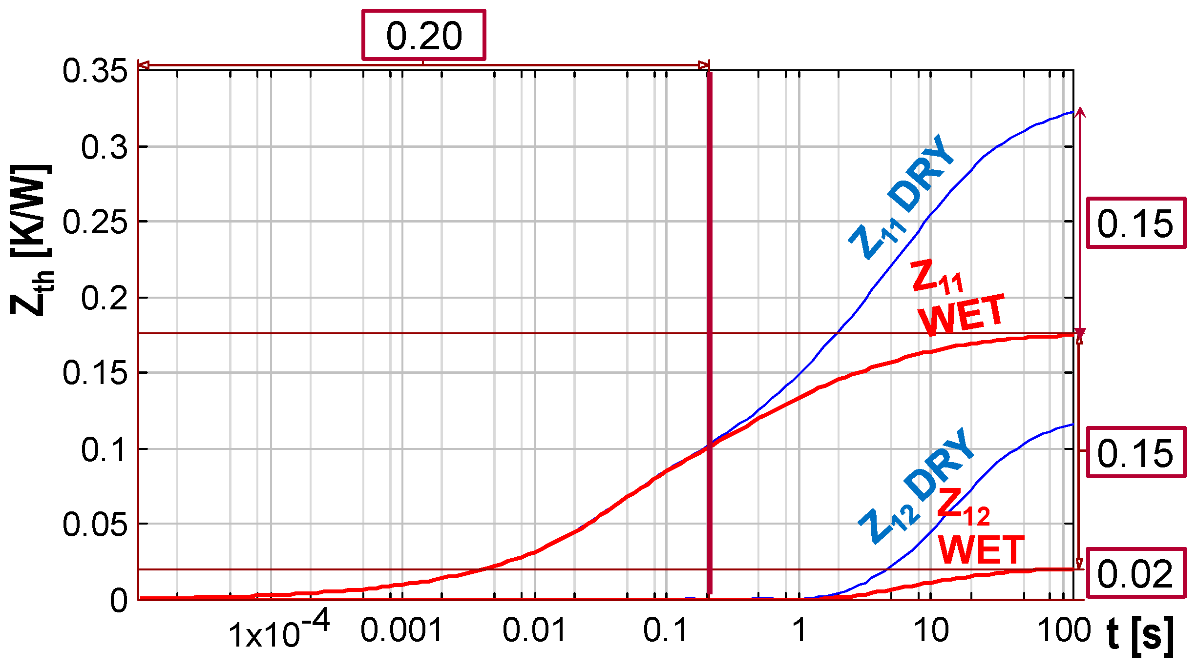
Figure 25 repeats the previous chart but now with the “wet” curves highlighted in red, thicker curves. For the “wet” case we obtain
R11 = 0.17 K/W thermal resistance for T1, and a transfer of
R12 = 0.02 K/W. This means that the good thermal contact of the base “decouples” the dice and we gain not only serious reduction of the thermal resistance but also much lower thermal stress resulting from the heating of other devices.
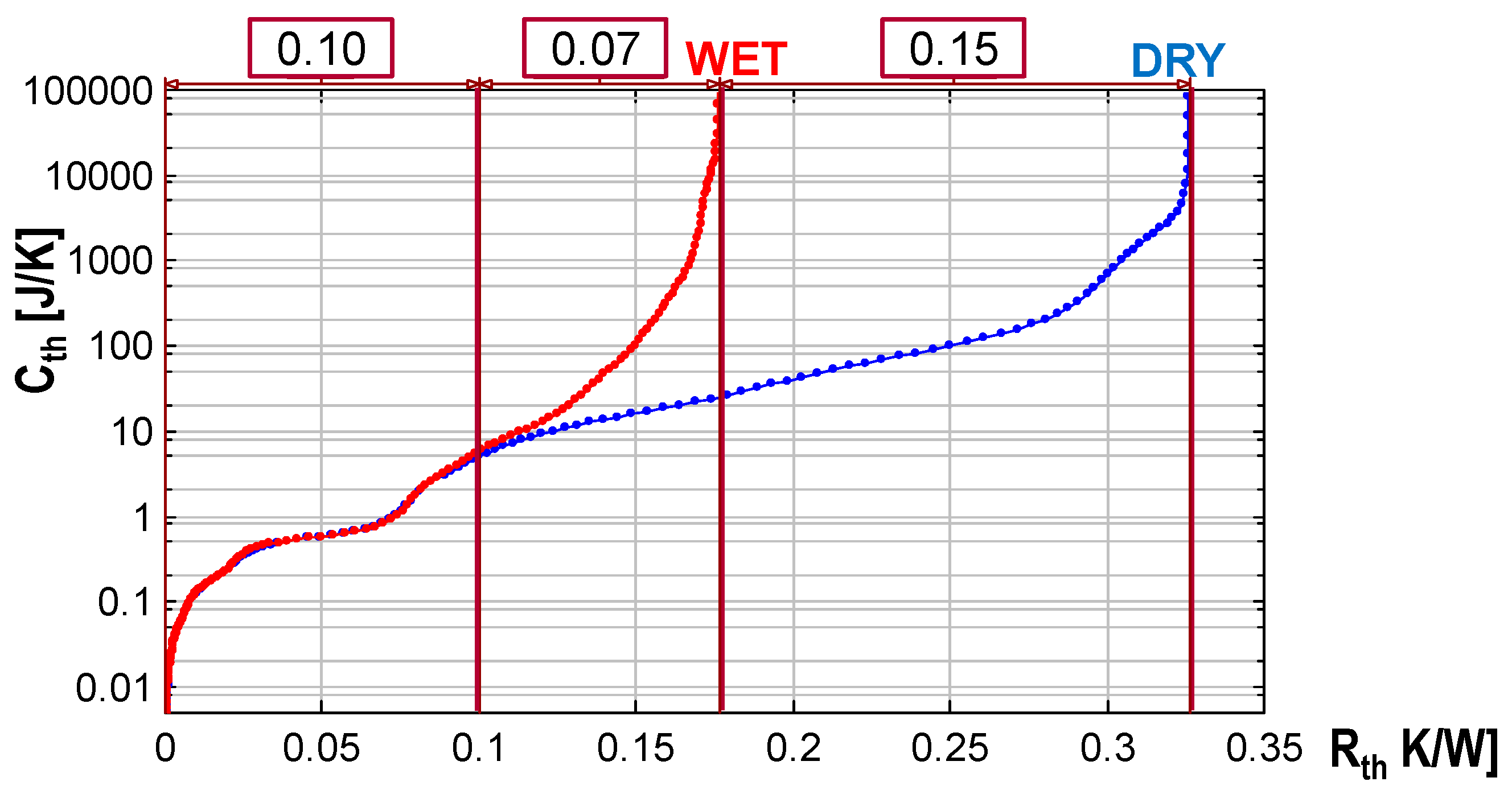
Figure 26 demonstrates the structure functions of T1. We can identify a junction to case thermal resistance of 0.1 K/W. The junction to ambient resistance improves from 0.32 K/W to 0.17 K/W, an improvement of 0.15 K/W, or 46%.
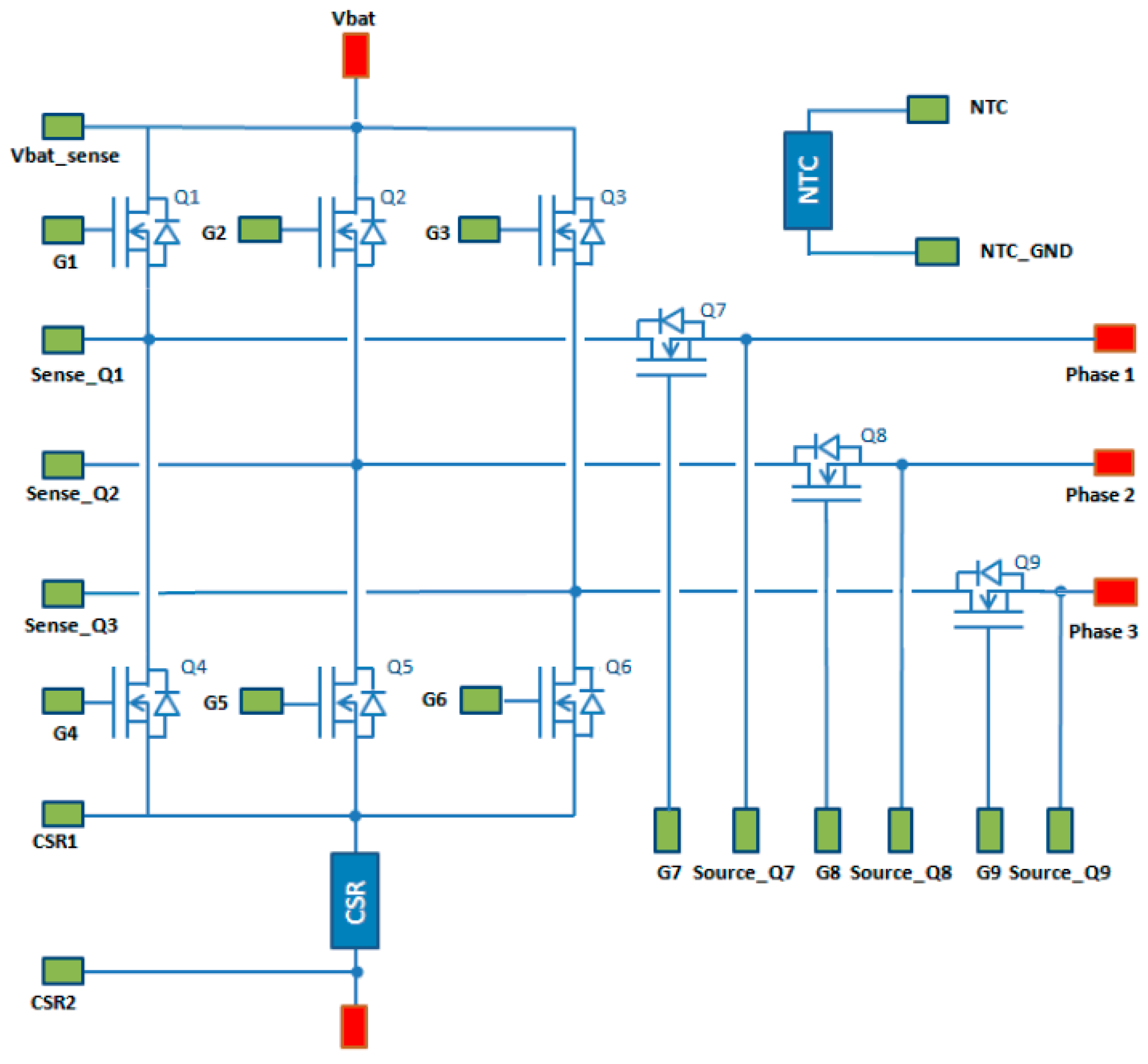
4.8. Testability of an Automotive Engine Control Unit Module
The circuit scheme of an automotive Engine Control Unit (ECU) module is shown in
Figure 27. When attempting to test it, we noticed that there is some access to most switching devices in the module. Unfortunately, this is rather an exception than a rule for power modules.
For structural analysis we need a relatively low power. For example, for the MOSFET devices in the upper row, namely Q1, Q2, and Q3, we have access through
Vbat and their emitter sense pins. The current is limited to a few amperes on the sense wiring, but this is more than enough to obtain crisp and reasonable structural results, as seen in
Section 3.3.
For reliability tests we need a much higher current. Accordingly, we can apply power only on transistor groups, e.g., Q1 + Q7, through Vbat and Phase1. This powering corresponds more or less to the normal operation mode of the module.
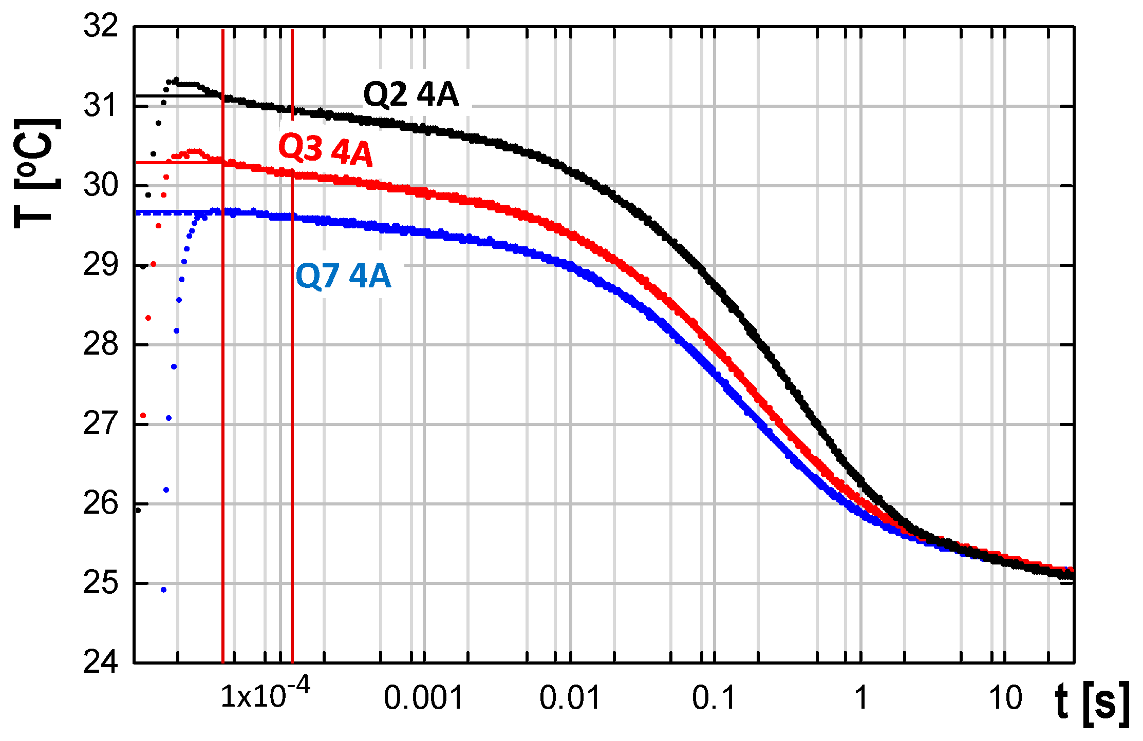
Figure 28 shows the recorded cooling transients on devices Q2, Q3, and Q7 at 4 A heating and 0.1 A sensing current. The resulting power step is approximately 3.3 W, which already produces a temperature change of 5 °C to 6 °C in a crisp and noise free manner.
The electric transients are to be corrected at around 30 μs, after which we observe a clean temperature-induced signal.
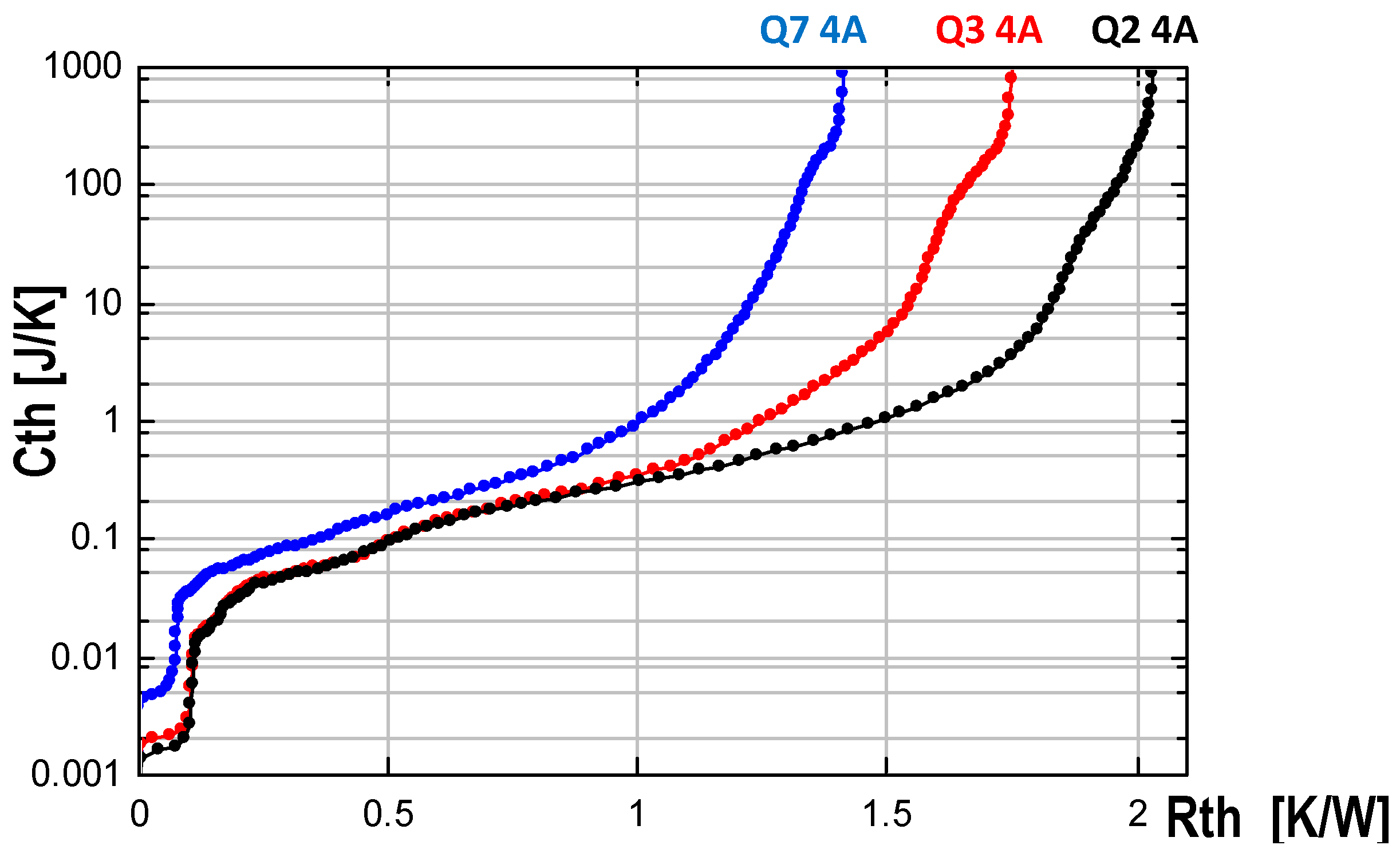
Figure 29 demonstrates the differences in the heat conducting path when the heat flow starts from Q2 or Q3, both in the upper row, or from Q7, sending the current towards
Phase1. All transistors were driven by 4 A. A faster increase of the structure function after the divergence point indicates that Q3 has better TIM coverage under the DBC plate than Q2, which has the same size. Q7 is a significantly larger transistor, as the early section of the structure function suggests.
5. Discussion
Thermal transient measurements offer a tool for identifying structural details in the heat conducting path belonging to a power assembly.
For the identification of structural details of an assembly, linearity of the thermal parameters (thermal conductivity, specific heat) has to be assumed, but no linearity of the electric behavior or the voltage-temperature mapping is needed.
The actual “thermally induced” nature of a transient can be verified by comparing a set of measurements at different heating and sensing currents and normalizing them with the power change during the test.
Although the well-established framework of existing thermal measurement standards is developed to extract a few characteristic parameters only, such as the junction to case thermal resistance of packages, still it helps in planning the structural analysis process.
Thermal transient testing standards prescribe recording the temperature of a single point on a single data acquisition channel of the test equipment. This technique is advantageous in many ways. First, all channel offset and gain errors of the equipment cancel out at the calibration process, so the only source of error is the deviation from the targeted thermostat temperature during calibration. On the other hand, as the change of the thermal resistance is negligible in the span of the measurement, a higher sensor current adds a constant (small) temperature shift to the actual transient, not influencing the calculations based on the change of the temperature.
The longest time interval where a transient of true thermally induced nature can be taken is with a high sensing current and low heating current, as such minimizing electric effects at the current change.
Although the powering and sensing occurs for a single device, the methodology can reveal the composition and integrity of remote structural elements.
The structure function method analyzed in the paper is not a technique that can be used without any preliminary knowledge of the structure. Relevant interpretation can be achieved in different ways:
- -
Knowing all internal geometries and material parameters a “synthetic” structure function can be built up, superposing slices of material with given thermal resistance and capacitance and comparing the measured structure functions to it;
- -
Thermal transients can be simulated on an approximate solid model and structure functions can be composed from those. Geometry and material parameters can be tuned until the simulated and measured structure functions match;
- -
Measured structure functions can be compared to an already identified “golden device”. This technique is rather advantageous in production control.
In complex power modules the heating current(s) may flow through more devices, and more dice can be used for sensing, applying a sensor current on them.
In cases of modules, an estimation can be given on the proportion of the internal power dissipation on the wiring based on the “accordion”-like shrinking of normalized cooling curves.
Transient testing can be used to analyze the heat transfer between several dice in a module and their thermal coupling, depending on the external cooling conditions.


