Abstract
Although an analytical design approach-based digital controller—which is essentially a deadbeat controller—shows zero steady-state error and no intersampling oscillations, it takes a finite number of sampling periods to settle down to a steady-state value. This paper describes the application of a derivative-free Nelder–Mead (N–M) simplex method to the digital controller for retuning of its coefficients intelligently to ensure improved settling and rise times without disturbing the deadbeat controller characteristics (i.e., no ripples between the sampling periods and no steady-state error). A switching-mode buck regulator working at 1 MHz in continuous conduction mode (CCM) is considered as a plant. Numerical simulation results depict that the N–M algorithm-based optimized digital controller not only shows improved steady-state and transient performance but also guarantees rigorous robustness against model uncertainty and disturbance as compared to its traditional counterpart, as well as the other optimized digital controller fine-tuned through other derivative-free metaheuristic optimization techniques, such as the genetic algorithm (GA). A system generator-based hardware software co-simulation is also performed to validate the simulation results.
1. Introduction
Tightly regulated DC-to-DC switching regulators are a requirement of modern low-power high-frequency (for enhancing the integration of devices and passive components) digital devices. Perturbations in input voltage or load current may keep the output voltage unregulated, thus reducing the devices life. There is a need to introduce a controller into the loop to keep the output voltage regulated, regardless of the changes in load current and input voltage. A direct discrete-time controller designed on the basis of an analytical design approach (synthesis rather than analysis approach) offers somewhat nominal performance. This paper proposes that better transient response and steady-state error characteristics can be achieved by retuning the digital controller coefficients using the Nelder–Mead local search algorithm.
Both emulation and direct digital design approaches are extensively used for constructing digital controllers for a wide variety of engineering applications. Reference [1] suggested a new discrete-time PID controller with a filter, combining the pole-zero cancellation (PZC) and inversion formulae-based analytical design control methodologies, for the buck regulator to ensure sufficiently large stability margins and superior performance. The method, however, involves heavy computations. Abbas et al. in Reference [2] successfully designed the phase lead-lag control theory-based digital controllers for the buck regulator, with consideration of all the control loop parameters. Reference [3] suggested a digital gain scheduling controller designed on the basis of lead-lag control theory for the modeled DC-DC series resonant converter for DC wind turbines, operating in continuous conduction mode (CCM). In Reference [4], for the sake of surmounting the difficulties in estimating discrete buck converter power stage parameters from noise, a new self-tuned Kalman filter (KF)-based parametric system identification technique was proposed. A direct digital design technique based PID controller was then applied to the identified buck converter to improve the tracking performance. The paper, however, lacks the detail of designing the PID controller. A unified nonlinear robust current observer for robust sensorless controllers of switching regulators was proposed in Reference [5]. Although the observer speeds up the tuning process, it requires a memory cheaper code. In Reference [6], based on the switched Lyapunov theory, a novel sampled-data control approach (essentially a digital control strategy) was developed for the buck converter working in CCM and DCM modes with variable switching frequency operation to ensure set-point tracking and stability. However, to realize the controller, a sampled data switched model for the converter has to be developed. In Reference [7], a sampled data controller was designed for a buck converter to realize the concept of sensorless control, with the help of direct digital control theory; it was targeted to minimize the output voltage fluctuations because of load variations.
Deadbeat control theory is also employed for the design of digital controllers for various engineering applications. In Reference [8], a discrete gain variable controller was designed on the basis of classical deadbeat control methodology, while the gain of nonlinear coupled equations was determined by using evolutionary techniques, such as the genetic algorithm along with the Newton Raphson method. The simple optimized deadbeat-controlled system shows comparable results with that of the finite control step method. In Reference [9] a single-input, single-output sampled data system was considered as a plant. Deadbeat control methodology was applied to minimize the cumulative time-weighted functions of tracking error in the frequency domain. The application of deadbeat control quickly reduces the error sequence. Two examples of sample data system were presented to show the performance of deadbeat control techniques. In Reference [10] polynomial-based control was applied for a double-boost converter. The controller was tested against the changes in source voltage and load resistance. It was found that, although the deadbeat controller had a great ability to track the error signal, it was more sensitive to parametric changes. Similarly, deadbeat control theory was employed to design a digital controller for an inverter of distributed generators. The current controlled deadbeat controller was designed in such a way to position the closed loop poles at the origin with a minimum disturbance input gain [11]. In all the above-mentioned references, the digital control laws are tuned using the traditional control theory for ensuring a nominal performance, which can be further improved using optimization techniques.
Numerous examples in the literature are reported where the digital control laws are optimized using the various advanced calculus-based or metaheuristic-based optimization techniques. For example, in Reference [12], the Levenberg–Marquardt (LM) algorithm-based nonlinear least squares optimization method was applied to PZC-based digital controllers for the buck regulator. The numerical results show tremendous improvement for the optimized controllers. Reference [13] suggested the dynamic PSO (dPSO)-based optimization of digital fractional order PID (FO-PID) controller applied to the buck converter fed DC motor for optimal speed control. Similarly, optimization techniques such as PSO was employed for optimizing the parameters of the fuzzy controller applied to the Quasi-Z Source converter [14] and for fine-tuning digital PID controller parameters [15]; the magnitude optimum criterion for developing explicit analytical tuning rules for digital PID controllers [16]; the genetic optimization scheme for improving a single-input fuzzy PID controller for the buck regulator [17]; the election campaign optimization algorithm for tuning digital PID controllers for the discrete-time system [18]; the gradient descent method for refining the digital control law for ac-to-dc converters to achieve unity power factor [19]. Similarly, in Reference [20], different swarm intelligence-based optimization techniques (i.e., an artificial bee colony, cuckoo search, etc.) were employed to get the enhanced speed and efficient maximum power point tracking algorithm for a photovoltaic system. Even promising derivative-free metaheuristic techniques are also subjected to limitations: The PSO suffers from the premature convergence problem like other stochastic algorithms; the GA requires coding the data to be in categorical form.
Well-recognized traditional control theory-based digital controllers, if optimized in an efficient way even with local search optimization methods, may offer excellent transient response and steady-state error characteristics. Motivated by this concept, this paper proposes the analytical design approach-based optimized digital controller. In this research, it was observed that the digital controller was optimized more efficiently with substantially fewer objective function evaluations by a simpler and derivative-free N–M method, as compared to other the derivative-free GA metaheuristic method. There are various factors responsible for the success of the N–M method over the other methods. It is simple in structure and performs deterministic transformations. The algorithm employs operations, namely, reflection, expansion, contraction and shrinkage while finding new lower points in the search space easily without using the information of derivatives. Ridges in the objective surface are easily traversed by the algorithm, while exploring the new lower points. This characteristic prevents the algorithm from converging too early. This justifies the applicability of the N–M method for optimizing the discrete-time controllers for switching converters. In addition, according to the best knowledge of the authors, the analytical design method has not been optimized by the N–M method.
The paper commences with the modeling of the buck switching converter to be controlled in Section 2. The complete design procedure of the analytical design approach-based digital controller is highlighted in Section 3. The suggested Nelder–Mead algorithm for optimizing digital controller is treated in Section 4. Comprehensive numerical simulation results with discussion are presented in Section 5. A cycle-accurate hardware-software co-simulation for fast prototyping is performed in Section 6. The findings of the paper are concluded in Section 7.
2. Buck Converter Modeling
A highly unregulated DC input voltage Vin got converted into a lowly regulated output voltage Vout using a buck converter, whose circuit diagram is shown in Figure 1. The circuit includes the unavoidable parasitic elements, like inductor DCR and capacitor ESR. DCR is the direct current resistance of inductor while ESR is the equivalent series resistance of the capacitor, denoted by RL and RC (in our case), respectively. An additional zero is introduced in the buck converter’s transfer function because of the ESR of the capacitor [21]. For the lossless buck converter, the input voltage Vin, the output voltage Vout and the switch duty ratio D are interrelated, over a period of steady-state operation, as:
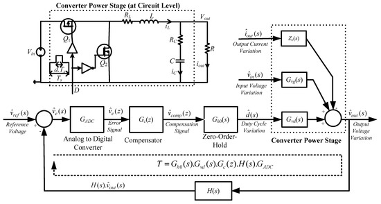
Figure 1.
Closed-loop digital control system block diagram (also including the circuit diagram).
The specifications of the buck converter to be considered throughout the paper are as the following: Vin = 3.6 V, Vout = 2.0 V, L = 6.8 µH, C = 6.8 µF, rL = 505 mΩ, rC = 50 mΩ, fs = 1 MHz, and Ts = 1/fs = 1 µs. The detailed block diagram (also including the buck converter circuit diagram) of the closed-loop digital control system is shown in Figure 1.
As can be observed from Figure 1, the output voltage variation is a linear combination of the input voltage variation , the load current variation and the small-signal duty cycle perturbation , propagated through the transfer functions, namely the line-to-output transfer function , the converter output impedance of the loaded power converter and the control-to-output transfer function , respectively. That is to say:
The three transfer functions , , and , derived using the state-space averaging technique [22,23], are expressed by:
With:
By the introduction of a feedback loop, the effect of and on can be diminished. The , with the feedback loop, takes the following form:
where the product of all the gains in the loop designated as loop gain is given by:
Here, and the sensor gain are considered in unity for the sake of simplicity. For a sufficiently large magnitude in loop gain , the last two terms of Equation (2) can be ignored, as they are reduced by a factor of . However, the first term suggests that, for the known DC reference and DC sensor gain , may precisely track provided that and . The first term, therefore, is responsible for the output voltage regulation and stability of the converter. Correspondingly, the control-to-output transfer function is considered as a plant for the digital controller design.
In order to design the direct digital design approach-based digital controller, the second-order analog buck converter needs to be discretized. The (which is actually ) preceded by the zero-order-hold (ZOH), for the component values mentioned above with a sampling period of 1 µs, can be discretized as:
3. Analytical Design Approach-Based Digital Controller
The analytically designed discrete deadbeat controller enforces the error sequence of a closed-loop control system to become zero on the application of the specific time-domain input signal. The output response of the feedback system exhibits minimum settling time, no inter-sampling ripples and zero steady-state error. The controller achieves the reference voltage in a quick and efficient manner. The analytical design approach-based digital controller algorithm [8,10,24] is explained by the following steps:
- 1.
- The analog transfer function of plant is firstly discretized by using one of the transformation techniques like ZOH (in our case), with the sampling period , as follows:
- 2.
- In order to have minimum settling time with zero steady-state error, the closed-loop transfer function described by Equation (13):should have finite impulse response as:where is the order of the overall system and is equal to or greater than the order of plant , and to are the coefficients of the impulse response of the closed-loop control system. From Equation (14), two deadbeat control criteria can be explored as follows:
- The sum of the coefficients of polynomial should be equal to 1, i.e., . This is actually the DC gain of the system.
- For the controller to exhibit the deadbeat response, all closed-loop poles should be forced at origin. This can be mathematically written as where is termed as the control system delay and is the integral multiple of with the minimum values of 1. It should be clear that should not contain any value with a positive term of z; otherwise the system responds before the input is applied, which is against the physical realization of the controller.
As the transfer function of the buck converter is of second order (n = 2) and the series expansion of starts with , the closed-loop pulse transfer function should be of the following form: - 3.
- The controller pulse transfer function can be derived by rearranging Equation (13) as:
- 4.
- In order to achieve the steady-state value with the limited number of sampling periods, the error sequence is described as the difference of the reference signal and the output signal:should be minimized in a quicker way. By substituting the discrete-time step input signal, Equation (17) can be written as:In order to achieve the steady-state value with a finite number of sampling periods, must be of the following form:where is a polynomial with finite terms in negative power of z. By rearranging Equation (19), can be written as:The solution of Equation (20) gives the quotient and the remainder as:
- 5.
- In order to avoid the inter-sampling oscillations after the steady-state is reached, must be of the following form:From Figure 1, can be written as:By substituting the unit step input and digitized plant in Equation (24), and for to be similar as in Equation (23), must be of the following form:The solution of Equation (25) gives quotient and remainder equations as:
- 6.
- As the controller forces the error sequence to zero with minimum sampling period and no inter-sampling oscillations as the steady-state is reached, both the remainder terms defined in Equations (22) and (27) must be equal to zero. And by solving simultaneously both the equations, the coefficient of can be calculated.
- 7.
- Thus, by substituting the coefficients of , the discrete time controller comes out to be:
This completes the design procedure of the controller.
4. Derivative-Free Nelder–Mead Simplex Algorithm
One of the direct search methods (DRMs), named the Nelder–Mead (N–M) simplex method is employed for fine-tuning of the digital compensator, designed on the basis of an analytical design approach. The method optimizes the compensator by minimizing the voltage error signal in a quicker way without considering the information of derivatives. The objective function, in a multidimensional space, considered for minimizing the cost (error signal) is the integral of the squared error (ISE) and is given by:
The N–M algorithm adopted here is proposed by Lagarias et al. [25] and does not use numerical or analytic gradients. Since no bounds (lower and upper) on decision variables are imposed, the optimization problem is essentially the unconstrained one. There is no guarantee of convergence of the algorithm to a local optimum.
The n + 1 points of n-dimensional simplex actually represent the solutions of the problem. Regarding the construction of a simplex around initial guess x0, each component x0(i) of x0 adds 5%. In addition to x0, n vectors constitute the elements of n-dimensional simplex. The algorithm employs four operations, namely, reflection, expansion, contraction and shrinkage during each of the iterations. At each iteration of the algorithm, the simplex modifies itself repeatedly according to the following way:
- 1.
- Vertices Representation: First of all, all points (vertices) in the current simplex are denoted by , .
- 2.
- Order: The vertices in the simplex are ordered such that . This implies that, refers to the best point whereas represents the worst point. At each step in the iteration, the current worst point is discarded and replaced by another point, which becomes part of the simplex.
- 3.
- Reflection: The reflection point is generated by:where represents the centroid of the n best vertices except and is calculated by:Correspondingly, is then calculated. If , gets accepted and replaces and the iteration is terminated.
- 4.
- Expansion: If , the expansion point is evaluated by:Eventually, is then calculated. If , is accepted and the iteration is terminated. Otherwise (if ), is accepted and the iteration is terminated.
- 5.
- Contraction: If , a contraction between and the better of and , is carried out.
- a.
- Outside: If , an outside contraction is performed. is calculated by:
Correspondingly, is calculated. If , is accepted and the iteration is terminated. Otherwise, a shrinkage is performed (step 6)).- b.
- Inside: If , an inside contraction is performed. is calculated by:
Correspondingly, is calculated. If , is accepted and the iteration is terminated. Otherwise, a shrinkage is performed (step 6)). - 6.
- Shrinkage: The n (new) points are generated by:is calculated. Thus, at the next iteration, , , …, constitute the vertices of the simplex.
The points that the algorithm might calculate in the procedure, along with each new possible form of simplex, are depicted in Figure 2. A bold outline represents the original simplex. The algorithm stops as the stopping criteria meet.
Figure 2.
Pictorial description of Nelder–Mead (N–M) simplex method.
The application of the N–M optimization method to the conventional deadbeat controller results in an optimized controller. By taking the initial point as a real vector or real array of the coefficients of the digital controller computed through analytical design approach, the algorithm starts minimizing the cost function (the integral of the squared error (ISE)) at each iteration and ultimately comes up with the updated coefficients of the digital controller. The first few iterations, in the same run, as they display during the progression of the algorithm, are highlighted in Figure 3. Inspection of the results of the optimization reveals a reduction of the cost function monotonically with each iteration, thus ensuring better set-point tracking. Unoptimized and optimized digital controllers are described in Table 1.
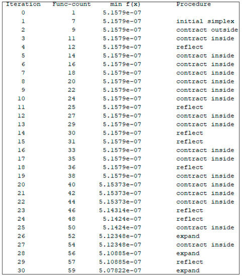
Figure 3.
First few iterations performed by the algorithm.

Table 1.
Unoptimized and optimized digital controllers transfer functions.
It should be noted that with the increase of problem dimension, the performance of the N–M method, however, deteriorates. This is because it has to count the objective function to be minimized a lot of the time, thus taking longer computational time.
5. Simulation Results and Discussion
In order to investigate the performance of the Nelder–Mead simplex algorithm-based optimized digital compensators and to show its supremacy over its unoptimized counterpart and the one optimized by other derivative-free metaheuristic techniques, such as the GA, numerical simulation results computed through MATLAB/Simulink environment are presented. A fixed-type solver is used for simulation purposes.
5.1. Nominal Performance
The optimized digital controller offered a much-improved output voltage response with a reduced rise, peak and settling times and overshoot than that of the conventional digital controller (see Figure 4). There is always a trade-off between the transient response characteristics and steady-state error characteristics. Improving one type of characteristics deteriorates the other type of characteristics. The Nelder–Mead algorithm, however, intelligently retuned the compensator coefficients without disturbing the deadbeat characteristics associated with Vout. The performance parameters offered by the optimized and unoptimized controllers are tabulated in Table 2.
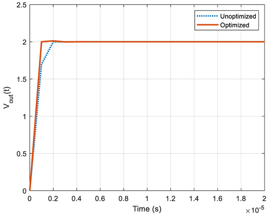
Figure 4.
Output voltage response offered by digital compensators.
Table 2.
Comparison of performance parameters.
In Figure 5, the control signal to the plant is also presented for the unoptimized and optimized compensated systems. As can be observed, a little bit more control effort was required, for the optimized case, to decrease the regulation times.
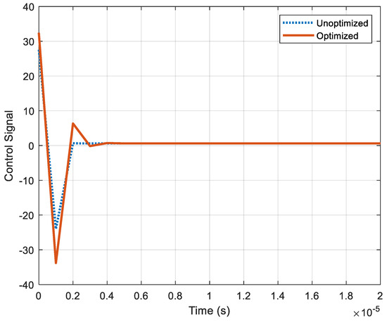
Figure 5.
Control signal to the plant.
Just for the sake of comparison and to investigate how other derivative-free metaheuristic techniques behave while fine-tuning the controller coefficients, another derivative-free metaheuristic technique, the GA, was employed to retune the controller coefficients. It is traditionally a well-known algorithm and becomes most effective (by evolving population) especially when very little information is available about the search. One can easily understand the concept of bio-inspired operators such as selection, crossover and mutation used by it. Further, it comes with the advantages of parallel search and random excursions. This is the reason for the selection of this algorithm for the comparison purpose. Of course, other metaheuristic algorithms could also be selected. The GA parameters used for the simulation purposes are tabulated in Table 3.
Table 3.
The genetic algorithm (GA) parameter values.
From Figure 6, it can be inferred that the GA could not perform better than the N–M method. It offered a relatively longer rise time and peak time of 1.1395 × 10⁻⁶ s and 4 × 10⁻⁶ s, respectively, with a larger overshoot of 23.8728%. In addition, as the deadbeat characteristics lost their nature, the controller optimized by the GA was no longer a deadbeat controller.
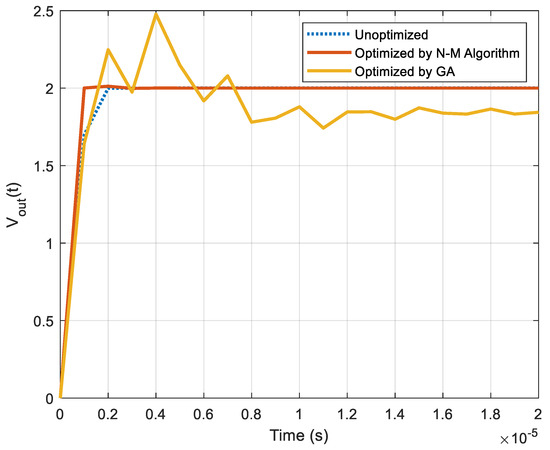
Figure 6.
Output voltage response offered by digital compensators.
The findings depict that the N–M method minimizes the unconstrained multivariable objective function (ISE in our case) more rigorously, compared to the GA metaheuristic approach. The successful optimized control solution suggests that the scorned DSMs deserve more attention from the optimization community.
5.2. Load Transient Response
The optimized controller (tuned by the N–M method) not only exhibited better nominal characteristics but also an excellent load transient response. For a change in load resistance from 4.5 Ω (iout = 444.44 mA) to 9.0 Ω (iout = 222.22 mA) and then from 9.0 Ω to 4.5 Ω, the optimized controller recovered more rapidly to its steady-state value with a peak to peak voltage spike of 63 mV, compared to the unoptimized controller, which offered 68 mV for the peak to peak voltage spike (see Figure 7). The optimized controller, therefore, showed more robustness against the variations in load current to maintain the output voltage at the desired level.
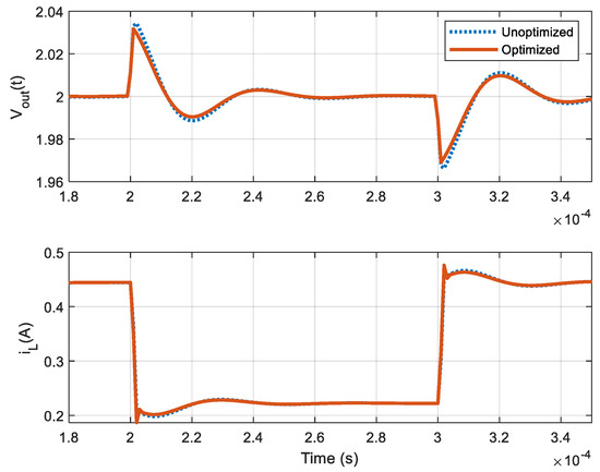
Figure 7.
Load transient response offered by digital compensators.
5.3. Disturbance Rejection
The variations in converter power stage parameters can be modeled by disturbance. For a step disturbance occurring at the plant input, the optimized controller rejected the disturbance quickly, without an increase of the overshoot, as compared to the unoptimized controller (see Figure 8). The optimized controller thus exhibited a good disturbance rejection capability.
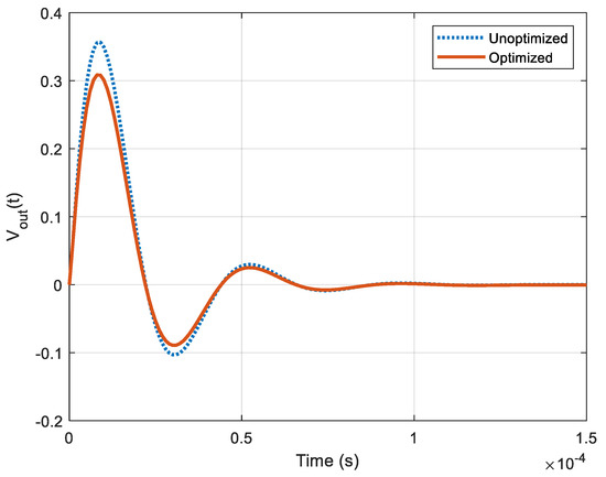
Figure 8.
Disturbance rejection performance offered by digital compensators.
5.4. Set-Point Tracking
The closed-loop set-point tracking demands that as . As can be observed from Figure 9, variations in the reference voltage from 2 V to 3 V and then from 3 V to 2 V was rapidly followed by the optimized digital compensator, with regard to its unoptimized counterpart, thus validating its significance.
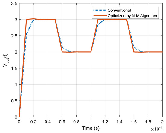
Figure 9.
Set-point tracking performance offered by digital compensators.
6. Hardware-Software Co-Simulation
The proposed optimized controller was also validated through hardware/software co-simulation using the Xilinx Artix-7 FPGA board (XC7A35T-1CPG236C) from Xilinx, Inc. (an American technology company), which was connected to a PC using a JTAG interface. To this end, a controller implementable model was developed using the Xilinx System Generator (XSG) toolset [26] in the MATLAB/Simulink environment. To test the XSG hardware controller, the error signal generated by the difference of reference signal and output signal, after digitization through ADC, in the Simulink environment, was made available to the controller using the “Gateway In” block. Similarly, the “Gateway Out” block was used to connect the controller output to the plant. These blocks performed the necessary data type conversions. This implies that some information may be lost during these conversions. However, the resolution of controller coefficients was of high significance, which may degrade the performance of the controller. Therefore, the controller coefficients were coded using single-precision floating-point data type, having a word length of 32 bits. With the successful model development, the executable bitstream was generated by the compiler, which was then downloaded into the FPGA board through the JTAG interface. Note that no VHDL code was required to be developed for testing the controller. Thus, the XSG-based hardware implementation shortens the development time drastically.
The steps in performing hardware/software co-simulation are as follows:
- 1.
- The optimized controller (described in Table 1) is re-written in the following form:
- 2.
- The above re-organized controller is converted into a difference equation as:
- 3.
- The controller described in Equation (30) or (31) is realized using adders/subtractors, multipliers, and delay elements from the XSG library as shown in Figure 10.
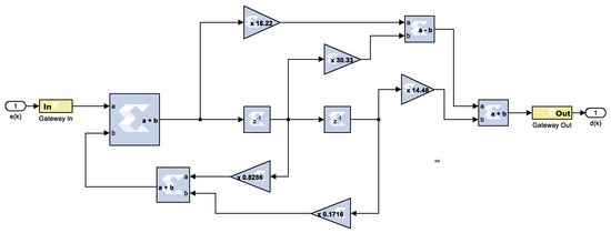 Figure 10. Digital controller realization using the Xilinx System Generator (XSG) library elements.
For realization of controller, standard programming was adopted, which uses n delay elements as compared to direct programming, which uses n + m, where n (n = 2) and m (m = 2 in our case) represent the number of poles and zeros respectively, such that n ≥ m [27].
- 4.
- The controller was inserted inside the control loop of the buck converter and the resulting model is shown in Figure 11.
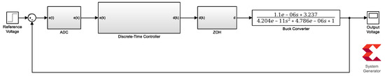 Figure 11. Closed loop representing hardware/software co-simulation.
 - 5.
- The overall model was compiled and the corresponding bitstream generated after the synthesis of VHDL code was downloaded into the FPGA. The situation of programming the FPGA is depicted in Figure 12.
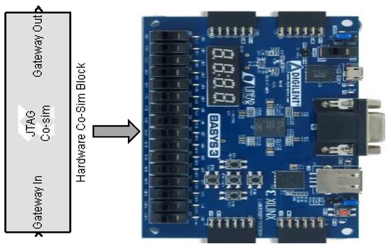 Figure 12. Bitstream to program the Xilinx Artix-7 FPGA board.
 - 6.
- Now, the output regulation of the controlled buck converter in a hardware/software co-simulation setting was analyzed. The regulation performance is depicted in Figure 13. It can be seen that the XSG-based controller exhibited a performance comparable to what was obtained during the simulations.
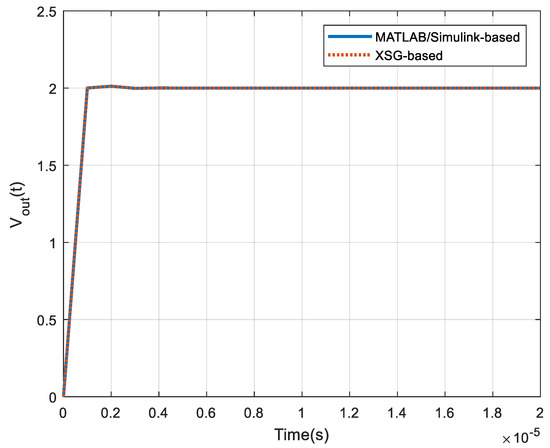 Figure 13. Response shown by the Simulink and XSG-based compensated system.
7. Conclusions
The paper suggests the application of the derivative-free Nelder–Mead simplex algorithm to the deadbeat control theory-based digital controller to ameliorate the performance. The nominally computed digital controller parameters were readjusted through the N–M algorithm. The optimized digital controller offered a superior load transient response, disturbance rejection, setpoint tracking and so on, compared to its unoptimized counterpart. While optimizing the controller, the deadbeat characteristics remained the same, but presented improved time-domain characteristics. Usually, an improvement in response times introduces overshoots, but this was not the case here. Like the GA, the N–M method does not involve operators like selection, crossover and mutation and thus was found to exhibit rigorous convergence characteristics. MATLAB/Simulink-based numerical results showed the superiority of the N–M method over the other derivative-free algorithms, like the GA. A system generator-based hardware into the loop implementation was performed to validate the simulation results. Variants of N–M method can be introduced, in the future, for further improvement in performance.
Author Contributions
Conceptualization, G.A. and J.G.; methodology, M.Q.N.; software, M.N.S.; validation, M.M.B. and A.R.; formal analysis, G.A., T.-C.L. and U.F.; investigation, G.A.; resources, V.E.B.; data curation, A.R. and U.F.; writing—original draft preparation, G.A. and M.U.A; writing—review and editing, U.F. and M.N.S.; visualization, M.M.B.; supervision, J.G.; project administration, M.U.A.; funding acquisition, V.E.B.
Funding
This research received no external funding.
Conflicts of Interest
The authors declare no conflict of interest.
References
- Cuoghi, S.; Ntogramatzidis, L.; Padula, F.; Grandi, G. Direct Digital Design of PIDF Controllers with ComPlex Zeros for DC-DC Buck Converters. Energies 2019, 12, 36. [Google Scholar] [CrossRef]
- Abbas, G.; Abid, M.I.; Farooq, U.; Gu, J.; Asad, M.U. Compensation of the Nonlinearities Present in the Digital Control Loop. In Proceedings of the 2016 International Conference on Intelligent Systems Engineering (ICISE), Islamabad, Pakistan, 15–17 January 2016; pp. 293–300. [Google Scholar]
- Chen, Y.-H.; Dincan, C.G.; Kjær, P.; Bak, C.L.; Wang, X.; Imbaquingo, C.E.; Sarrà, E.; Isernia, N.; Tonellotto, A. Model-Based Control Design of Series Resonant Converter Based on the Discrete Time Domain Modelling Approach for DC Wind Turbine. J. Renew. Energy 2018. [Google Scholar] [CrossRef]
- Ahmeid, M.; Armstrong, M.; Gadoue, S.; Al-Greer, M.; Missailidis, P. Real-Time Parameter Estimation of DC–DC Converters Using a Self-Tuned Kalman Filter. IEEE Trans. Power Electron. 2017, 32, 5666–5674. [Google Scholar] [CrossRef]
- Cimini, G.; Ippoliti, G.; Orlando, G.; Longhi, S.; Miceli, R. A Unified Observer for Robust Sensorless Control of DC–DC Converters. Control Eng. Pract. 2017, 61, 21–27. [Google Scholar] [CrossRef]
- Yan, X.; Shu, Z.; Sharkh, S.M.; Wu, Z.; Chen, M.Z.Q. Sampled-Data Control with Adjustable Switching Frequency for DC-DC Converters. IEEE Trans. Ind. Electron. 2018. [Google Scholar] [CrossRef]
- Song, P.; Cui, C.; Bai, Y. Robust Output Voltage Regulation for DC–DC Buck Converters Under Load Variations via Sampled-Data Sensorless Control. IEEE Access 2018, 6, 10688–10698. [Google Scholar] [CrossRef]
- Maher, R.A.; Aljebory, K.M. Design and Implementation of a Discrete Variable Gain Controller Based on a Numerical Approach. In Proceedings of the 2017 14th International Multi-Conference on Systems, Signals Devices (SSD), Marrakech, Morocc, 28–31 March 2017; pp. 566–573. [Google Scholar]
- Vargas, F.J.; Salgado, M.E.; Silva, E.I. Optimal Design of Ripple-Free Deadbeat Controllers Based on an ITSE Index. In Proceedings of the 18th Mediterranean Conference on Control and Automation, MED’10, Marrakech, Morocco, 23–25 June 2010; pp. 401–406. [Google Scholar]
- Veerachary, M.; Taffesse, F. Deadbeat Controller for Double-Boost DC-DC Converter. In Proceedings of the International Conference for Convergence for Technology-2014, Pune, India, 6–8 April 2014; pp. 1–5. [Google Scholar]
- Wang, J.; Song, Y.; Monti, A. Design of a High-Performance Deadbeat-Type Current Controller for LCL-Filtered Grid-Parallel Inverters. In Proceedings of the 2015 IEEE 6th International Symposium on Power Electronics for Distributed Generation Systems (PEDG), Aachen, Germany, 22–25 June 2015; pp. 1–8. [Google Scholar]
- Abbas, G.; Gu, J.; Farooq, U.; Abid, M.I.; Raza, A.; Asad, M.U.; Balas, V.E.; Balas, M.E. Optimized Digital Controllers for Switching-Mode DC-DC Step-Down Converter. Electronics 2018, 7, 412. [Google Scholar] [CrossRef]
- Khubalkar, S.; Chopade, A.; Junghare, A.; Aware, M.; Das, S. Design and Realization of Stand-Alone Digital Fractional Order PID Controller for Buck Converter Fed DC Motor. Circuits Syst. Signal Process. 2016, 35, 2189–2211. [Google Scholar] [CrossRef]
- Ranjani, M.; Murugesan, P. Optimal Fuzzy Controller Parameters Using PSO for Speed Control of Quasi-Z Source DC/DC Converter Fed Drive. Appl. Soft Comput. 2015, 27, 332–356. [Google Scholar] [CrossRef]
- De Moura Oliveira, P.B. Design of Digital PID Controllers Using Particle Swarm Optimization: A Video Based Teaching Experiment. IFAC Pap. OnLine 2018, 51, 298–303. [Google Scholar] [CrossRef]
- Papadopoulos, K.G.; Yadav, P.K.; Margaris, N.I. Explicit Analytical Tuning Rules for Digital PID Controllers via the Magnitude Optimum Criterion. ISA Trans. 2017, 70, 357–377. [Google Scholar] [CrossRef] [PubMed]
- Yuan, Y.; Chang, C.; Zhou, Z.; Huang, X.; Xu, Y. Design of a Single-Input Fuzzy PID Controller Based on Genetic Optimization Scheme for DC-DC Buck Converter. In Proceedings of the 2015 International Symposium on Next-Generation Electronics (ISNE), Taipei, Taiwan, 4–6 May 2015; pp. 1–4. [Google Scholar]
- Wenge, L.; Deyuan, L.; Siyuan, C.; Shaoming, L.; Zeyu, C. Tuning Digital PID Controllers for Discrete-Time System by Election Campaign Optimization Algorithm. In Proceedings of the 2010 International Conference on Mechanic Automation and Control Engineering, Wuhan, China, 26–28 June 2010; pp. 2559–2562. [Google Scholar]
- Zhang, W.; Feng, G.; Liu, Y.F.; Wu, B. New Digital Control Method for Power Factor Correction. IEEE Trans. Ind. Electron. 2006, 53, 987–990. [Google Scholar] [CrossRef]
- Ahmed, J.; Salam, Z. An Enhanced Adaptive P&O MPPT for Fast and Efficient Tracking Under Varying Environmental Conditions. IEEE Trans. Sustain. Energy 2018, 9, 1487–1496. [Google Scholar]
- Forouzesh, M.; Siwakoti, Y.P.; Blaabjerg, F.; Hasanpour, S. Small-Signal Modeling and Comprehensive Analysis of Magnetically Coupled Impedance-Source Converters. IEEE Trans. Power Electron. 2016, 31, 7621–7641. [Google Scholar] [CrossRef]
- Middlebrook, R.D.; Cuk, S. A General Unified Approach to Modelling Switching-Converter Power Stages. In Proceedings of the 1976 IEEE Power Electronics Specialists Conference, Cleveland, OH, USA, 8–10 June 1976; pp. 18–34. [Google Scholar]
- Tian, S.; Lee, F.C.; Li, Q.; Yan, Y. Unified Equivalent Circuit Model and Optimal Design of V2 Controlled Buck Converters. IEEE Trans. Power Electron. 2016, 31, 1734–1744. [Google Scholar] [CrossRef]
- Ogata, K. Discrete-Time Control Systems; Prentice Hall: Upper Saddle River, NJ, USA, 2012. [Google Scholar]
- Lagarias, J.; Reeds, J.; Wright, M.; Wright, P. Convergence Properties of the Nelder--Mead Simplex Method in Low Dimensions. SIAM J. Optim. 1998, 9, 112–147. [Google Scholar] [CrossRef]
- Xilinx Inc. System Generator for DSP. December 2014. Available online: http://www.xilinx.com/tools/sysgen.htm (accessed on 25 March 2019).
- Chakraborty, S. Analysis and Design of a Digitally Controlled Current Source Based Multi-Output Converter; University of Minnesota: Minneapolis, MN, USA, 2006; p. 318. [Google Scholar]
© 2019 by the authors. Licensee MDPI, Basel, Switzerland. This article is an open access article distributed under the terms and conditions of the Creative Commons Attribution (CC BY) license (http://creativecommons.org/licenses/by/4.0/).