1. Introduction
Measurement of partial discharges (PD) is nowadays conventionally used as the diagnostic method for medium and high voltage electrical devices [
1]. The method is primarily intended for the measurement of insulation quality and localization of isolation defects in MV and HV cables, instrument transformers and rotating machines. However, research in this field is still ongoing and the full use of PD diagnostic methods is a matter of the future [
2]. The most commonly used method of partial discharge measurement is the galvanic method according IEC 60270, which is very accurate and sensitive in comparison with other options [
1]. However, the accuracy of this method depends heavily on the level of interferences from the surroundings, the quality of the pulse discrimination system (PDS), input filter settings and last but not least on well performed calibration [
3,
4]. Most modern systems for PD measurement are equipped with a PDS. The suppression of interference from the surroundings is allowed by the PDSs, which are based on eliminating signals not coming from the tested objects. An example may be our Haefely DDX 8003 PD system (Haefely Hipotronics, Brewster, NY, USA), which can use two measuring channels and the antenna for the elimination of external influences. The piezo ultrasonic microphone may be an alternative to external corona elimination for other systems. Internal partial discharges occur in all tested objects from the initial voltage value and they are the most often created at sites of mechanical isolation faults, in the areas of material impurities, mechanical cracks and gas bubbles [
4]. PD calibrators are used for the purpose of the calibration process, which is described in
Section 2. In addition, physical calibrators can also be used to replace a test object with a defined failure. The defined fault in the test object causes a PD with a certain charge value, amplitude symmetry and phase spectrum depending on the applied voltage value. Knowledge of the PD amplitude and phase spectrum of predefined faults is the basis for its diagnostics in real objects. The aim of this research is to create a database of MV and HV cable faults simulated by physical calibrators and their verification. The verification of simulated faults was performed using the circuit calculation. The circuit is simulated in the Electronic Workbench software and the static state calculations before and during the fault are performed in Matlab Simulink software.
2. Calibration Process
The calibration process must be performed before each PD measurement. Each change of the measured circuit (change of the measured object, interconnecting conductors, input filter settings) leads to a change in the conditions of RF current pulses propagation that are generated by the failure in the test object [
4]. The calibration process involves injection of a known amount of charge into the test object electrodes with the use of standard external calibrators. The value of charge is an order of magnitude consistent with the expected value of the measured object. One or more pulses are generated by these calibrators within one period of the power grid signal and their amplitude is related to the size of the set charge level of partial discharge and capacity of coupling capacitor of PD measuring system. Calibration impulses can be also generated synchronously with the power line frequency. This feature is provided by advanced calibrators, such as the Tettex 9520 (Haefely Test AG, Basel, Switzerland). The calibration is always based on the creation of pulses predefined by the calibrator, which is parallel connected to the tested object. The principle of the calibration process is the assignment of the absolute value of the PD charge
QP or
QIES by the measuring system to the set charge value generated by the calibrator.
Calibrators can be realized as external devices or may be formed by impulse generators and the HV injection capacitors. For the PD system, these impulses are identical to the impulses formed inside of the tested object. Unfortunately, the creation of impulses by test objects is significantly more complex. PD within the test objects causes charge flows from the space charge of the dielectric to the point of failure. The part of the charge is also compensated from the power supply, or from the PD system coupling capacity. Moreover, only this part of the charge is expressed as the high frequency current impulses, which are measured by the system [
1].
However, most of external calibrators are able to calibrate only the charge level, but without consideration of fault location inside the test object. Flows of charges inside the test object are influenced by the location of the fault. The level of asymmetry of charge value within the positive and negative polarity is generally caused due to unbalanced faults with respect to the electrodes (ground electrode and HV out electrode). The measured PD charge value of real objects is changed depending on the position of the discharge location relative to the input electrodes. An example may also be medium or high voltage cables according to IEC 62067:2001. The measured value of the charge is also dependent on the position of the calibrator at the beginning or the end of the cable. The value can vary by approximately 20% at 20 m MV cable. Overall, the accuracy and sensitivity of the measurement is influenced by the asymmetry and complexity of the measured object structure. The asymmetric localization of a partial discharge in the measured object affects the symmetry of the phase spectrum in the positive and negative polarity parts. Simulation of these phenomena is impossible by standard low voltage calibrators. That is also why our calibrator was developed, which allows setting the PD charge value, producing more different pulses within one period and operating at the nominal voltage level of the test objects. Asymmetrical failures can be simulated as well. In the paper, a design and implementation of extended external galvanic calibration systems for the PD measurement is described. The proposed calibrators are based on numerical models of partial discharge inside the solid dielectric materials, but they are also designed as the physical models represented by the capacity networks and mechanically modified solid dielectric materials. Tested MV cable samples were mechanically damaged to form faults. The position of faults in damaged cables coincided with the fault position simulated by the calibrator. Also, more than 10 used cables with failures were tested and analyzed. These disorders originated naturally—by local mechanical and thermal degradation and aging of the insulation material. The test results at different voltage levels have proved the ability of the calibrated measuring system to locate insulation defects.
2.1. Currently Used PD Calibrators
All currently used calibrators are based on a simple low voltage generator of impulse or saw-tooth voltage waveform with a defined polarity and the voltage level. Examples are the Tettex 9520 calibrator and the Robinson Miniature Discharge 753US-1PD simulator (Haefely Test AG, Basel, Switzerland). Most of these calibrators are supplied from the internal accumulators. Therefore, they are implemented with galvanic separation. The principle of these modern calibrators is described in [
5]. Generating asymmetrical or partially symmetrical pulses and the value of the charge in the PD depending on the supplied voltage is not possible by none of the commercially offered calibrators. Moreover, normal laboratory calibrators cannot work as a reference, with exact dependencies of the PD value on certain HV voltage level. PD calibrators developed in our laboratory meet the following parameters. These calibrators can also be connected in parallel to the test object at nominal voltage or they can be used separately for collecting information into a failure knowledge database.
2.2. Physical Calibrator Requirements
The aim of the physical calibrator is the simulation of charge caused by the failure on real test objects. The calibrator must be designed for the same test voltage as the test object (nominal voltage of power distribution networks components, e.g., 10 kV or 22 kV). The range of the produced charge should be from units of pC for insulators and HV cables, up to tens or hundreds of nC for power transformers and mechanically more complex objects. Requirements for the calibrator are summarized in the following points:
The operating voltage difference potential from 0 V to approximately 30 kV AC.
The option to choose the location of the fault (symmetrical or asymmetrical).
Setting the charge value of PD in the range of 0.1 to 1000 pC depending on the applied voltage.
Low corona design and easy reconfigurability of charge value parameters or fault position.
3. Schematic and Numerical Model of Calibrator
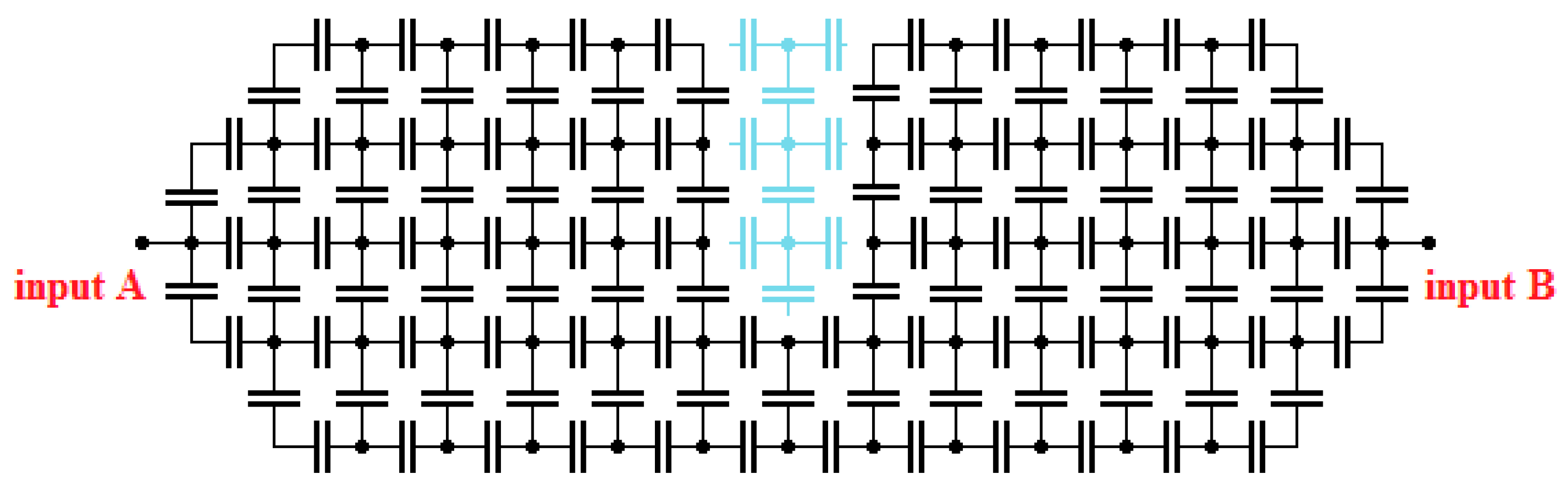
The new calibrators are based on the capacitor network. Electrical parameters (dissipation factor, permittivity) of commonly used ceramic or PP high voltage capacitors are approximately identical with the properties of solid PE, XLPE dielectrics. We suppose that the model dielectrics can be implemented as a flat (2D) or three-dimensional (3D) arrangement of electronic elements. The 3D model corresponds more to the reality of the measured objects parameters, however, the possibilities of its implementation and parameters settings are more complicated for users. The flat model is a sufficient solution for PD simulation and testing of measurement systems. In addition, rotationally symmetric objects can be satisfactorily replaced by this 2D model. The capacitor network is realized with a certain step that corresponds to the physical dimensions of the real dielectric in the order of several tenths or units of mm.
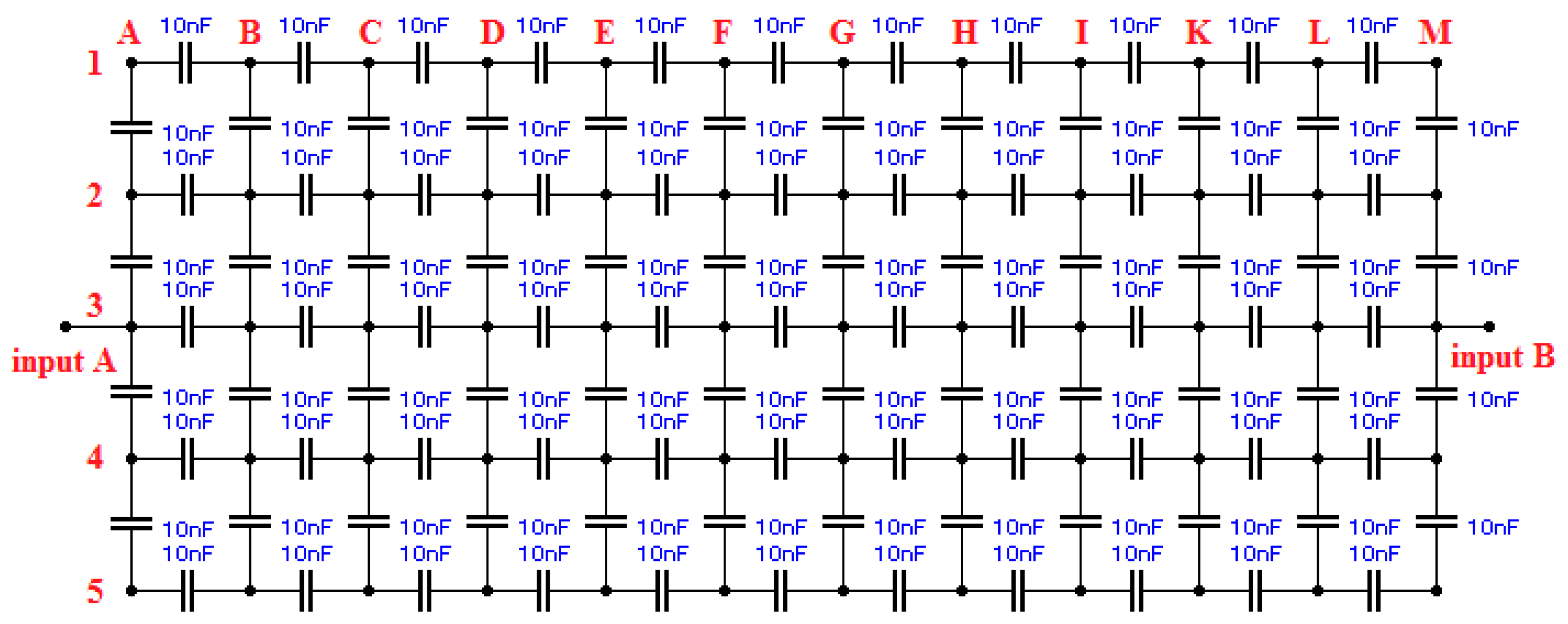
The network of our Calibrator “Model A” is implemented as flat model with 5 × 12 partition steps. PD, breakdowns or short circuits between the junctions can be implemented with an external circuit, which can be connected between any junctions of the circuit. Schematic of this network for simulating is shown in
Figure 1. The numerical calculation of individual model nodes is performed in Matlab software, Matlab Simulink is used to calculate steady state.
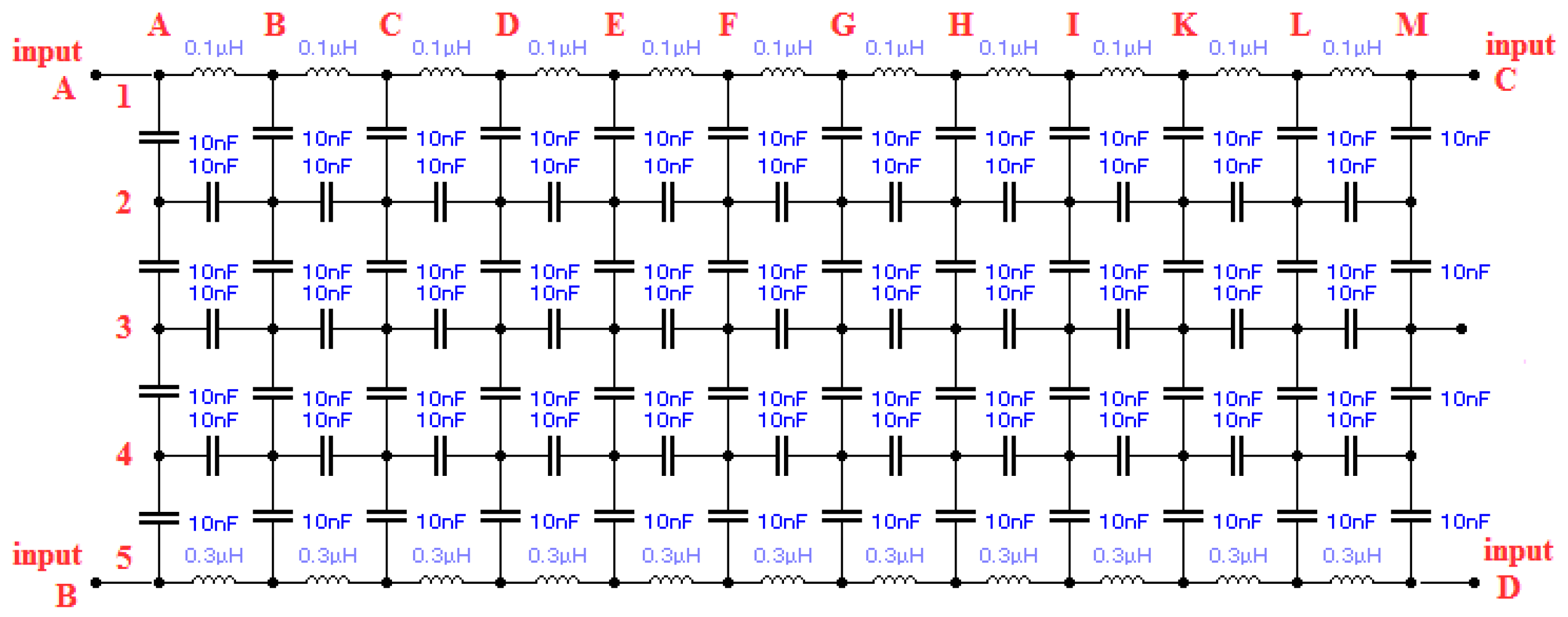
The second calibrator “Model B” is designed and implemented as a three-dimensional device. This model is made of transparent solid PMMC dielectric material. Part of the circuit between input electrodes is removed and can be replaced by other solid, liquid or gaseous dielectrics. The last calibrator “Model C” is the latest and most sophisticated. This calibrator is a flat model of MV cable and its scheme is shown in
Figure 2. The design of “Model A” and “Model C” calibrators was based on knowledge of [
6,
7,
8] and the physical dimensions of the MV cable faults.
Capacitance and inductance values are selected based on the experience, physical properties of PE and XLPE used dielectrics and applicable simulation values. The one step capacity corresponds to the order of about 0.3 mm of a XLPE material. Values of partial inductances are determined by experimental measurement of core and shielding inductance of 20 kV 185 mm2 MV cables.
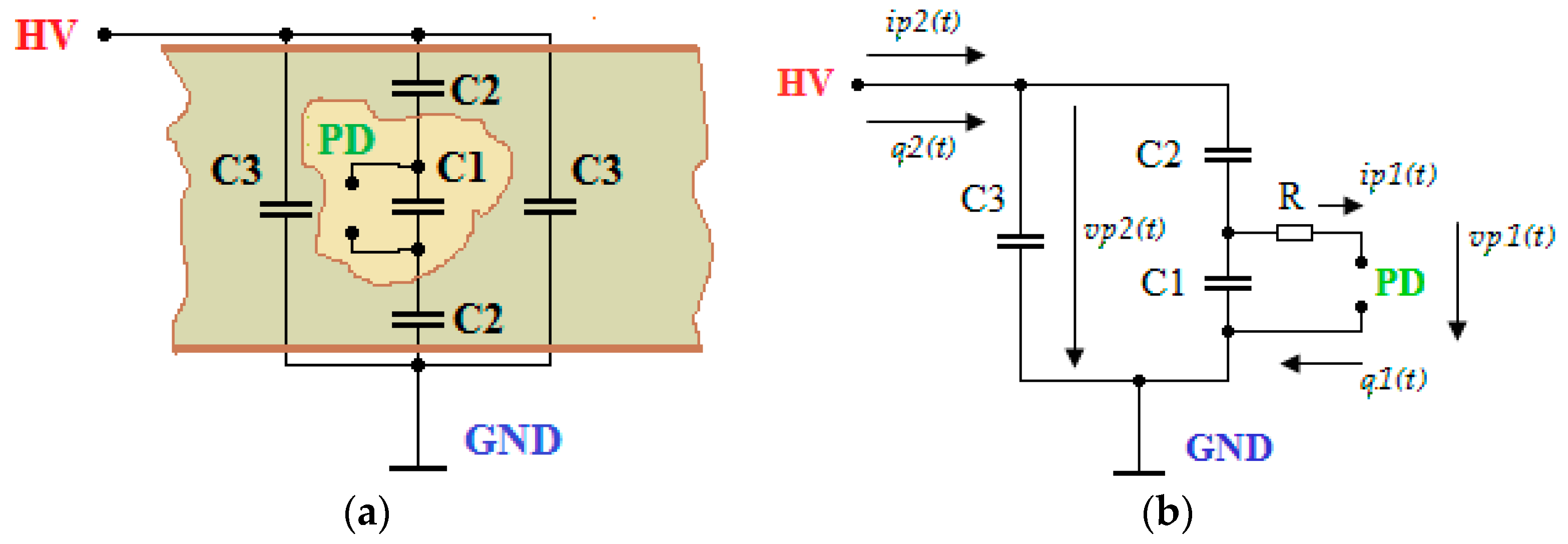
The simulation of PDs is performed by a fast change of part capacity between two junctions. The behavior of the circuit is based on the Gemant and Philippoff model [
9]—three capacitance circuit schematically illustrated in
Figure 3. More precise models can be based on Böning [
3,
10]—five capacitance model or Eberhard Lemke dipole model based on Paderson assumptions [
2].
The part of the charge is then quickly transferred in the calibrator components. Thus the fast current impulse is flowing from the supply circuit to compensate the change of capacitance charge. These impulses can be created several times during one period. This type of PD can be simulated numerically by quickly short connecting two junctions in the capacitor model for a short time period. This connection can be synchronized with the phase of the applied voltage period. The practical implementation of a fast, lossless switch is complicated. In a physical model, using fast, voltage controlled semiconductor elements or gas filled overvoltage protections is recommended.
At present, “Models A” and “C” were designed, simulated, implemented and laboratory tested. The first “Model A” is formed by a network of capacitors and allows simulating the partial discharge in one or more places between junctions at the same time or within one period. The model allows creation of a partial discharge q2(t) with a set value from 0.1 to 1000 pC. This PD can be created in a variety of locations nearby the input electrodes, in the central part of the model or on its sides. The calculation of overall charge q2(t) change is possible by the simulation software (e.g., Electronic Workbench software). The external circuit can be turned on at the set value of voltage vp1(t). The value of the voltage is proportional to the parameters of the impurities in the material, to the physical size of the inclusions and the mechanical failures and their chemical composition. Thus the real behavior of dielectric material is simulated in this way.
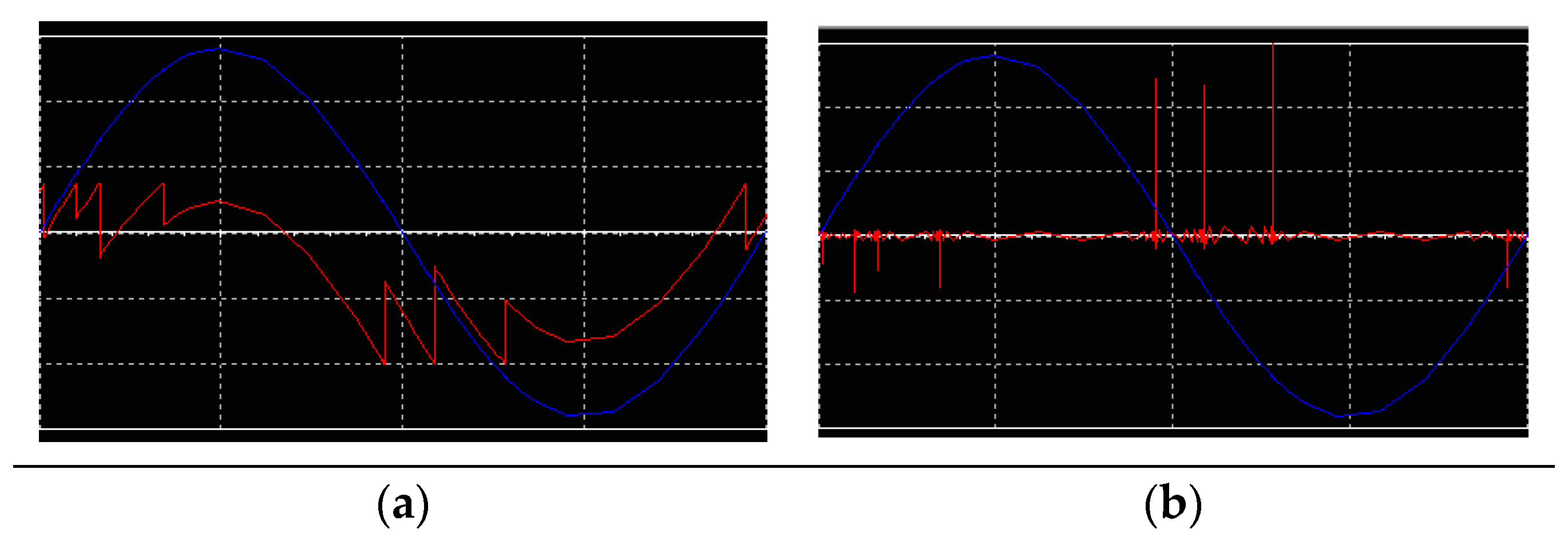
Most of the faults in real objects are not symmetrical. Typically, they are not located in the vicinity of the axis of the object or its central part. They can be also located at its edges or near the input electrodes. The voltage drop on the fault or the current taken from the power supply is not symmetrical. An example may be the connection of external circuit between 2B and 2C junctions. The set peak value of PD
q2(
t) is 10 pC. The voltage drop on the external circuit
vp1(
t) and the impulse current
ip2(
t) taken from the power supply is shown graphically in
Figure 4. Red curve—voltage drop waveform on fault and current pulses, blue curve—waveform of applied voltage.
The rotationally symmetrical 3D “Model B” is implemented purely from a dielectric material. The electrical diagram of this model in the flat section is shown in
Figure 5. Also, it is possible to use the ANSYS software simulator to determine the approximate values of transferred PD charge. However, this model is mainly experimental for verification and comparison of the different dielectric and composite material properties. The model is partially based on the experience of [
11].
4. Implementation of a Physical Model
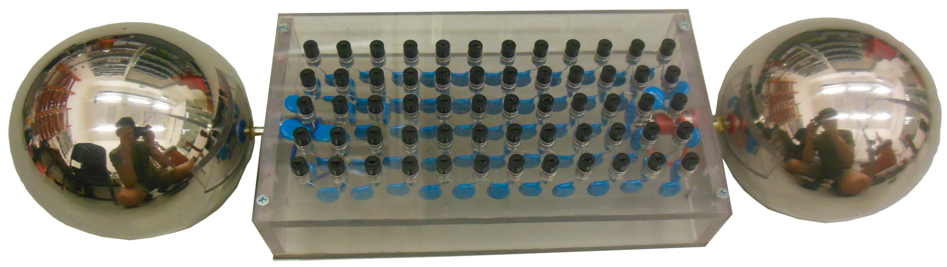
“Model A” is made of 10 nF ceramic capacitors type CC81 with a low dissipation factor < 0.5%. The maximum voltage of the “Model A” is 30 kV and the maximum voltage drop
Vp1 between two junctions is about 3 kV in the idle state. However, the simulations showed that the impulse voltage drop
vp1(
t) on the capacitor at current impulse of PD can reach up to 7.5 kV. Therefore, capacitors with a nominal voltage of 10 kV were chosen. The value of the transferred charge
q2(
t) is dependent on the choice of PD location and the settings of the threshold voltage
vt1(
t) of the ignition system. The model is designed for a wide range of transferred charge
q2(
t) from 0.1 to 1000 pC. Low corona connection is provided by the external spherical electrodes. And this model offers an easy option of reconfiguration and setting the correct value of pC with the help of software simulators. All 60 junctions are available for connecting the ignition system. The model also allows for creation of asymmetric faults. The physical realization of the “Model A” is shown in
Figure 6.
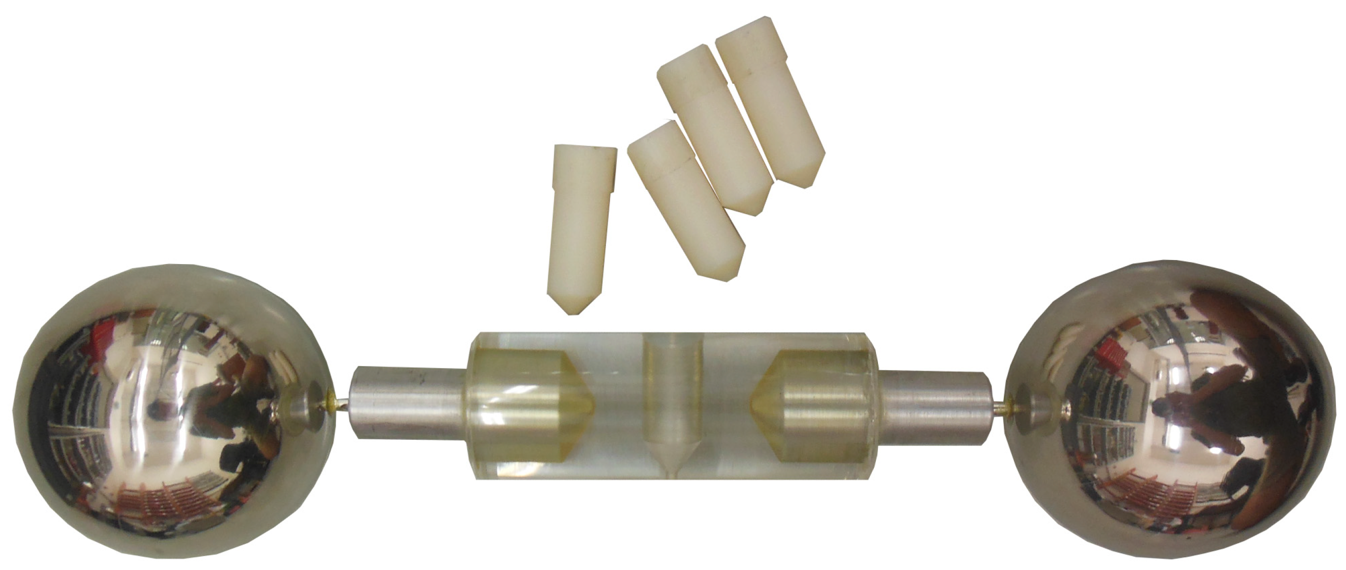
Physical Calibrator “Model B” is designed for voltages up to 50 kV AC (100 kV with external electrodes). However this model is less sensitive in comparison with “Model A” and “C”. Overall, the “Model B” is designed and implemented as a rotationally symmetric capacitor with a small radial cavity in the middle. It is possible to insert test materials into the cavity (homogeneous materials, inhomogeneous, porous, with air or gas bubbles etc.). The photo of the latest version of “Model B” is presented in
Figure 7.
The input electrodes of “Model B” are made of aluminum in conical design. The construct material is a homogeneous cylinder of PMMC. Into the radial cavity located in the middle of the cylinder, it is possible to insert other kinds of solid or porous materials. Inhomogeneous electric field is produced in the vicinity of the input electrode. However, the electric field becomes uniform in the direction to the cavity. The formation of PD is minimized inside a homogeneous part of cylinder and discharged are appearing only in the cavity. Mineral oil or petroleum jelly can be used to prevent the formation of undesirable PD in the transition of the air gaps between the cylinder material and the tested material. The design of the model prevents the formation of the external corona of up to 100 kV between the external electrodes. Corona is eliminated by the smooth design of the model. For very accurate measurement with very low PD background noise of 150–200 fC at 100 kV in frequency range of 50 to 500 kHz, it is possible to use the external spherical input electrodes.
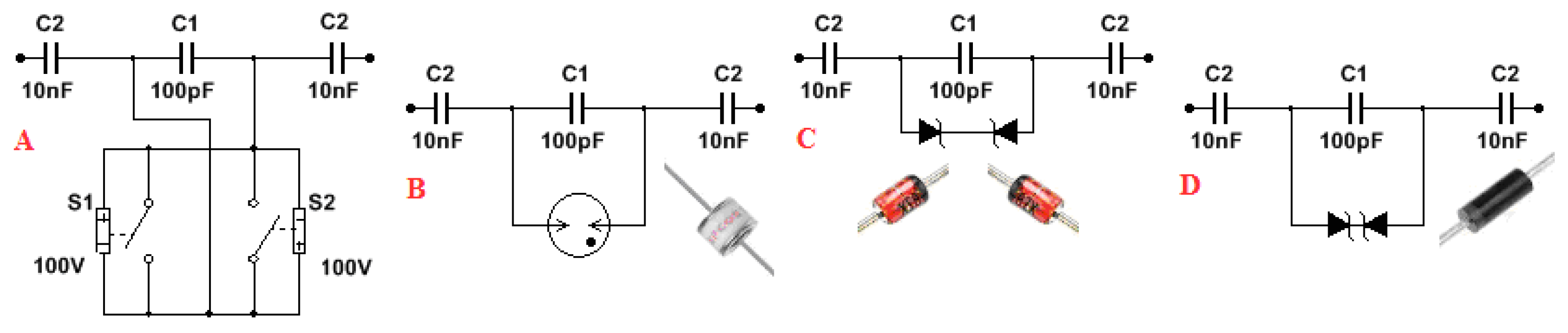
Ingnition System of the External Circuit
The ignition system is designed for the “Models A” and “C”. The purpose of this ignition system is to ensure the relocation of the charge
q1(
t) within the test object. The charge
q1(
t) is determined by the ignition voltage and the value of the capacity C
1, which can be shorted. The ignition voltage can be set from the units of Volts to the hundreds of Volts. Coupling capacity can be chosen from pF to tens of nF. It is possible to drive the ignition system by fast electronic circuit. However, a simpler solution is to use same of different Zener diodes “C”, transils “D” or gas surge protections “B”. The disadvantage of this solution is only one set value of the ignition voltage. For the change of charge or ignition voltage values, it is necessary to change the electronic component coupling capacitors C
2 or value of working capacitor C
1. All electronic schematics of the tested ignition system are shown in
Figure 8. In all cases the value of the transferred charge
q1(
t) it is possible to determine for one ignition of the PD (one current pulse
ip1(
t)) or for all the impulses within one period. The charge change value
q1(
t) at the fault location or the charge change value
q2(
t) of the whole calibrator circuit can be determined by calculation or SW simulation.
Capacitors C
2 are coupling and capacitor C
1 is a working one. Only this capacitor is shorted by the ignition system and the shorted differential charge
q1(
t) is compensated by an external circuit. The part of differential charge
q2(
t) is also compensated by power supply circuit with coupling capacitor and this part of charge is measured by PD meas. systems. Therefore, there are also differences between the ignition value set of charge
q1(
t) and the charge
q2(
t) measured by the PD meter in external circuit. The first Circuit “A” in
Figure 8 is a theoretical circuit, which is used for the purpose of simulation. This circuit is implemented with two fast electronic relays, which are set to a threshold voltage level
vp1(
t) =
vt1(
t) in both polarities. Unfortunately, mechanical relays are not fast enough for practical use. Gas discharge tube surge arresters or neon tubes are used in the circuit “B”. This solution proves to be the most reliable, fastest, and most similar to the actual partial discharges. Alternative circuits are the circuits “C” and “D” that use symmetrical or asymmetrical fast semiconductor components with a fixed value of the ignition voltage
vt1(
t). In our case—mainly fast and powerful 600 W or 1.2 kW transils are used for most practical measurements.
5. Laboratory Verification of Simulators Function
Verification of functionality, parameters settings and determination of deviation from simulated parameters of all calibrator models were carried out using:
Haefely Hipotronics DDX 7000 with internal calibrator, 1 nF coupling capacitor CB and 100 pF injection capacitor CI. Measurements were performed in the frequency range 20–200 kHz with a background of approx. 0.8 pC.
Haefely Hipotronics DDX 8003 with pulse discrimination system PDS and external calibrator Tettex 9520 in frequency range 20–200 kHz with background of approx. 0.5 pC.
Tettex DDX 9121b with coupling impedance AKV 9310 and external calibrator Tettex 9520 in frequency range 50–500 kHz with background of 0.15 pC.
Calibrator “Model A” has been validated on the accuracy of setting the level of the measured charge
q2(
t) by Tettex DDX 9121b. The value of pulse
q2IEC(
t) charge taken from the power supply circuit was set by the ignition system. The value of the charge has been determined by simulation. For simplicity, only one pulse per period or two pulses per period in the symmetric partial discharges have been used. The value of maximum error is 30% for DDX 8003 and 20% for DDX 9121b. The results of simulation and measurement are described in
Table 1. All these values are for two pulses per one period. The generated pulses by “Model A” and “C” pulses are very similar to PD of MV cables. The pulse width at 50% amplitude is between 5 and 10 µs, thus they are easily detectable by PD detectors with a frequency range of 20 to 500 kHz.
The charge value PD is given either as a peak value Qpeak (QP) or as a QIEC value according the IEC standards, which is the largest repeatedly occurring PD magnitude. The QIEC value is the most commonly reported value in simulations or measured in measuring devices.
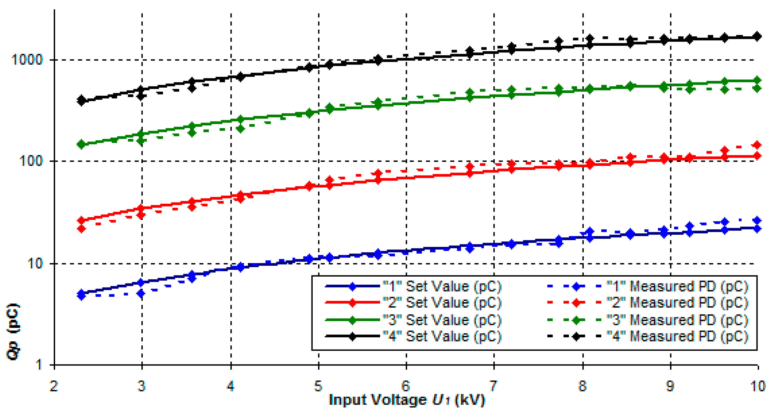
Simulated PD values are calculated for voltage range 2.3 to 10 kV of input voltage
V1. All practical measurements were performed on “Model A” and measured by DDX 8003. The result of the measurement is the verification of the correct function of the physical calibrator “Model A” in the whole range of simulated charges from pC to nC. The measurement results are shown graphically in
Figure 9. The test also included a withstand voltage test and a corona test at a maximum voltage of 30 kV. Corona did not appear in practical measurements.
The differences between the set PD values by calibrator simulation and the measured values by PD meas. systems are small (deviation max. 30% for DDX 8003). The identification of individual simulations corresponds to
Table 1. The measurements made by the PD meter DDX 9121b are even more accurate. Calculated deviations are in the order of several percent or tens of percent. These laboratory measurements demonstrated the functionality of the “Model A” in a wide range of configurations and different voltage levels.
Simulation of symmetric and asymmetric faults on “Model C” has also been successful. Malfunctions of insulation condition of MV cables were simulated in the range of 0.5 to 5 pC. The deviations between the simulation and the measured values are about 10%. The data obtained from this model will be used as samples of standardized MV cable faults in the database system.
The Calibrator “Model B” is designed for the measurement of tested material properties. Four different solid materials were selected for testing in the Calibrator “Model B”. The measured values for the individual materials are shown in
Table 2.
Measurements of Calibrator Model B have shown that this device is sensitive enough to measure inhomogeneities, cracks and gas cavities in homogeneous solid insulating materials. This calibrator is therefore mainly suitable as a demonstration tool for simulating partial discharges in solid dielectric materials, for example, used in MV and HV power cables. Again, data for material samples can be stored in the database system for future comparison of measured samples or mutual comparison of different samples.
6. Discussion and Conclusions
This article summarizes the basic information of our long-term research activities in the design, implementation and practical measurement of PD using non-traditional partial discharge calibrators. The purpose of these calibrators is to imitate real test objects more accurately than electronic calibrators. For the time being, the measurements of very low PD values (below 5 pC) in MV cables by these calibrators have also proved to be beneficial. Also, collecting the examples of amplitude and phase spectra for predefined faults of MV cables is of great benefit.
Above all, the possibility to use this type of calibrators for mutual relative comparison of different systems makes it a unique tool for laboratory use, further research in MV and HV cables, new dielectric materials and sensitive PD measurement systems. The simulation possibilities of individual processes in the insulation dielectric materials are a suitable tool for final student’s thesis (bachelor’s, master’s or dissertation thesis). Also in addition, it is possible to use these calibrators for practical laboratory exercises and precise measurement for simulations and practical verification of set parameters and PD on voltage dependences.
The features and options of the Calibrators “Model A” and “Model C” allow the simulation of all possible faults as in the real objects, especially MV cables and instrument transformers. One or more symmetrical or asymmetrical partial discharges can be simulated at the same time, within one period. The “Model B” allows testing the real materials and measuring their properties. Calibrator “Model B” can be used to measure other electrical parameters such as permittivity and dissipation factor in combination with an electronic bridge. And the main measured parameter is a partial discharge depending on the applied voltage. The sensitivity of the “Model B” is sufficient for measurements from 100 fC.
Further development of these calibrators will be directed to increasing the sensitivity, the elimination of external influences and the option settings. Another goal is to reduce the errors between the software simulations and the practical settings of the calibrators.
Author Contributions
Conceptualization, M.K.; Data curation, L.P., J.S. and J.O.; Formal analysis, L.P.; Investigation, L.P.; Methodology, M.K. and J.S.; Project administration, J.O.; Validation, L.P.; Resources, I.K.; Supervision, J.O.; Writing-original draft, M.K. and L.P.; Writing-review & editing, J.O. and I.K.
Funding
This research was funded by the Ministry of Education, Youth and Sports of the Czech Republic under OP VVV Programme (project No. CZ.02.1.01/0.0/0.0/16_013/0001638 CVVOZE Power Laboratories—Modernization of Research Infrastructure).
Acknowledgments
Authors gratefully acknowledge the Centre for Research and Utilization of Renewable Energy (CVVOZE) in the research infrastructure CVVOZEPowerLab.
Conflicts of Interest
The authors declare no conflict of interest.
References
- IEC 60270: High-Voltage Test Techniques, Partial Discharge Measurements, Consolidated Version with Amendment 1, Ed. 3.1; IEC: Geneva, Switzerland, 2015.
- Lemke, E. A critical review of partial-discharge models. Electr. Insul. Mag. 2012, 28, 11–16. [Google Scholar] [CrossRef]
- Mentlik, V.; Pihera, J.; Polansky, R.; Prosr, P.; Trnka, P. Diagnostika elektrických zařízení; BEN—Technicka Literatuta: Prague, Czech Republic; 439p, ISBN 978-80-7300-232-9.
- Heller, R. Aspects of Partial Discharge Measurement; University of West Bohemia: Pilsen, Czech Republic, 2007. [Google Scholar]
- Fidan, M.; Ismailoglu, H. A Novel Partial Discharge Calibrator Design via Dual Microcontroller and High Speed DAC. In Proceedings of the ELECO’2007 5th International Conference on Electrical and Electronics Engineering, Bursa, Turkey, 5–9 December 2007. [Google Scholar]
- Gunnarsson, O.; Bergman, A.; Rydler, K.E. A Method for Calibration of Partial Discharge Calibrators. IEEE Trans. Instrum. Meas. 1999, 48, 453–456. [Google Scholar] [CrossRef]
- Gupta, A.K.; Ray, S. Modeling of Calibration Circuit for Partial Discharge Measurement. Bacherol’s Thesis, Department of Electrical Engineering, National Institute of Technology Rourkela, Odisha, India, 2013. [Google Scholar]
- Kimt, K.H.; Yi, S.H.; Lee, H.J.; Kang, D.S. Setup of standard PD calibrator and its uncertainties. J. Electr. Eng. Technol. 2011, 6, 677–683. [Google Scholar] [CrossRef] [Green Version]
- Gemat, A.; Philippoff, W. Die Funkenstrecke mit Vorkondensator. Z. Für Tech. Phys. 1932, 13, 425–430. [Google Scholar]
- Böning, W. Luftgehalt und Luftspaltverteilung geschichteter Dielektrika I. In Electrical Engineering (Archive fur Elektrotechnik); Springer: Berlin, Germany, 1963; Volume 48, ISSN 0948-7921, online ISSN 1432-0487. [Google Scholar]
- Chen, G.; Baharudin, F. Partial Discharge Modeling Based on Cylindrical Model in Solid Dielectrics. In Proceedings of the International Conference on Condition Monitoring and Diagnosis, Beijing, China, 21–24 April 2008; IEEE: Pisctaway, NJ, USA, 2008. ISBN 978-14-2441-621-9. [Google Scholar]
© 2019 by the authors. Licensee MDPI, Basel, Switzerland. This article is an open access article distributed under the terms and conditions of the Creative Commons Attribution (CC BY) license (http://creativecommons.org/licenses/by/4.0/).

 ,
, 
