Article

A Comparative Study of S-S and LCCL-S Compensation Topologies in Inductive Power Transfer Systems for Electric Vehicles

Department of Electrical Engineering, Chonnam National University, 77, Yongbong-ro, Buk-gu, Gwangju 61186, Korea
*
Author to whom correspondence should be addressed.
Energies 2019, 12(10), 1913; https://doi.org/10.3390/en12101913
Submission received: 8 April 2019 / Revised: 26 April 2019 / Accepted: 16 May 2019 / Published: 18 May 2019
(This article belongs to the Special Issue Wireless Power for Electric Vehicles)

Abstract

:
In inductive power transfer (IPT) systems, series–series (S-S) and double capacitances and inductances–series (LCCL-S) compensation topologies are widely utilized. In this study, the basic characteristics of S-S and LCCL-S are analyzed and compared in the tuning state. In addition, considering the universality of detuning, and because the two topologies have the same secondary structures, the voltage and current stress on components, input impedances, voltage gains, and output powers of S-S and LCCL-S are mainly analyzed and compared in the detuning state, which is caused by variations in the secondary compensation capacitance. To compare the efficiency of the two topologies and verify the comparative analysis, comparative experiments based on a 2.4-kW IPT experimental prototype are conducted. The comparative result shows that the S-S compensation topology is more sensitive to load variations and less sensitive to secondary compensation capacitance variations than LCCL-S. Both in the tuning and detuning states, the efficiency of the S-S topology is higher in high-power electric vehicle (EV) applications, and the efficiency of LCCL-S is higher in low-power.

1. Introduction

To solve the environmental pollution problems and ensure the continuous reduction of traditional energy usage, new energy industries have emerged, and are being developed rapidly, especially in the electric vehicle (EV) industry [1,2,3]. As the core technology of EVs, there have been constant breakthroughs in inductive power transfer (IPT) technology [4]. IPT technology can be employed to realize power transmission from a power source to load devices in a non-contact way via the coupling magnetic field between the primary and secondary coils [
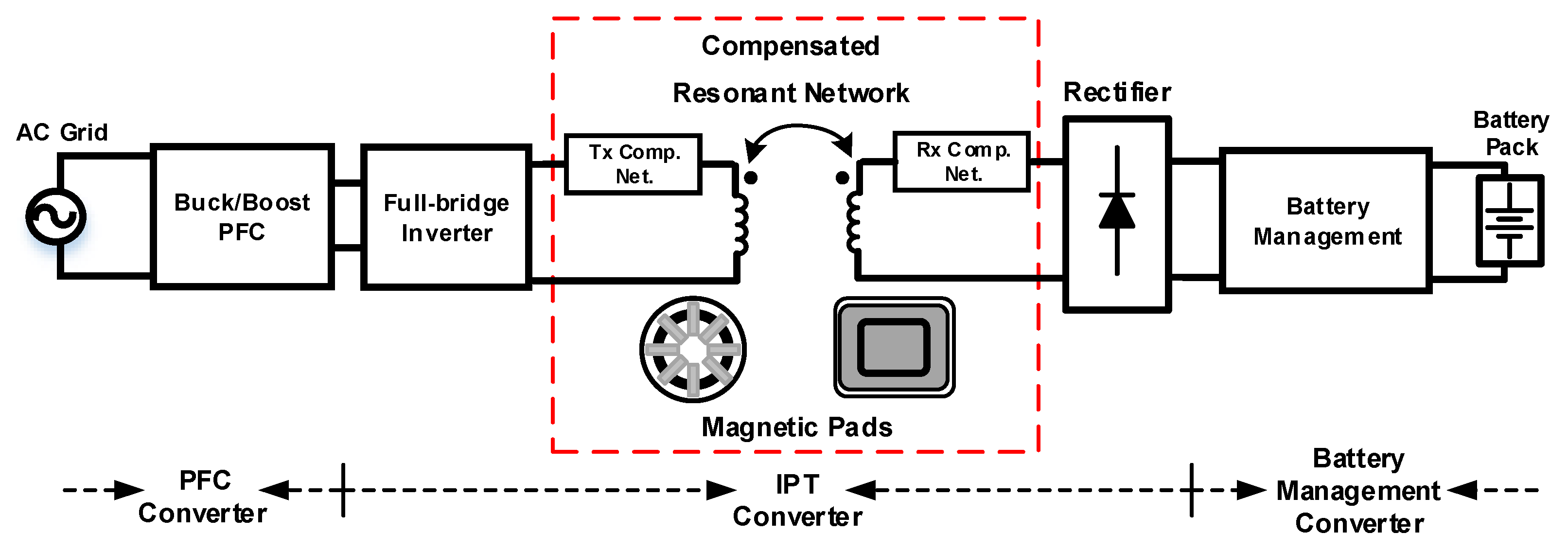
5]. A typical IPT system diagram is shown in Figure 1. Without the need for direct electrical contact between the primary and secondary sides, IPT technology has the advantages of good environmental adaptability, safety, convenience, and smaller size [6,7]. Thus, it largely compensates for the shortcomings associated with conventional cable charging [8].
In IPT systems, resonance compensation topology is a key component that directly affects the system performance and charging quality [9,10]. Conventional basic resonance compensation topologies include series-series (S-S), series-parallel (S-P), parallel-parallel (P-P), and parallel-series (P-S) [11]. Recently, there have been several studies and analyses on these four resonance topologies, and researchers have begun to try some new topological combinations and analyze some high-order resonance topologies.
In [12], a new resonant topology called S-CLC are proposed, which has advantages, such as constant output voltage, ease of implementation of zero phase angle (ZPA) [13], and zero voltage switching (ZVS). In [14], the design procedure of an optimized parameter for LCCL-S resonant topology is reported. Using the optimized design, high efficiency ZVS operation over an entire load range can be achieved. Meanwhile, comparative studies of different resonance topologies have been reported in some literature. In [15], under the condition of mutual inductance variations that are caused by misalignment, the S-S and double-sided LCC topologies are compared in terms of output power, efficiency, voltage, and current stress. Based on the analysis and experiments, although the conclusion is that S-S has a higher sensitivity and component stress than double-sided LCC as mutual inductance varies, only double-sided LCC experiments are performed. In [16], using a varying coupling coefficient k (0.18–0.26), the design methods, volumes, costs, complexities, and efficiencies of series LC (SLC) and hybrid series parallel (LCL) topologies are compared, and the results prove that the LCL topology has higher efficiency, lower capacitance stress, and control complexity than the SLC topology.
During the application of IPT technology, detuning is a universal issue [17,18]. Although an ideal charging efficiency can be obtained near the ZPA frequency, the resonance state can easily be broken because of detuning. In both detuning and tuning states, the characteristics and performances of the topology vary significantly [19]. Detuning is mainly caused by two factors. First, owing to the improper parking of EVs, there are usually misalignments between transmitting and receiving coils, leading to a large drop in the mutual inductance (coupling coefficient) and minor variations in the self-inductances. Secondly, during actual operation, because of high temperatures, oscillations, device manufacturing errors, and some other physical factors, actual parameters (compensation capacitances and inductances) may differ from designed parameters. Both detuning reasons may cause ZPA frequency deviations. Although the compensation topologies may be under the same detuning condition, there are often differences in the actual impacts caused by detuning on different compensation topologies. Therefore, the analysis and comparison of the characteristics of different topologies in the case of detuning not only has practical significances, but can also help to optimize the parameter design of compensation topologies.
In terms of the detuning studies, most of the studies are concerned with detuning that is caused by misalignment between primary and secondary coils. However, there are few studies on detuning that is caused by deviations in compensation components. Therefore, in this study, because S-S and LCCL-S have the same series structures in a secondary loop, the characteristics of S-S and LCCL-S are not only compared in the tuning state, but also compared in the detuning state, which is caused by variations in the secondary compensation capacitances. The deviation factor of the secondary compensation capacitance is defined. The related equations of S-S and LCCL-S in the detuning state are then derived. Next, similarities and differences between the two topologies are compared and summarized based on the excel calculation results. In addition, because it is difficult to compare the efficiencies of S-S and LCCL-S by performing calculations and simulations, a 2.4-kW experimental prototype is configured to compare the efficiencies of S-S and LCCL-S compensation topologies.

2. Theoretical Analysis of Compensation Topologies

2.1. Basic Characteristics and Analysis of the S-S Topology

Figure 2 illustrates the circuit analysis topology model of the S-S compensation topology. Us is the equivalent AC input voltage (output voltage of the Full-bridge (FB) inverter) of the compensation topology, and according to Fourier theory, the relational expression between Us and UDC (DC-link voltage of IPT system) can be defined as:
U s = 4 U D C π n = 1 , 3 , 5 sin ( n ϕ ) n
In (1), n is the label of the odd harmonic, and ϕ is the frequency corresponding angle of Us. During the analysis of this study, only the fundamental harmonic (n = 1) is considered. Rac is the equivalent AC load resistance. According to [20], when the output low-pass filter only consists of capacitors, the relationship between Rac and the rectifier output resistance (RL) can be defined as:
R a c = 8 π 2 R L
For the primary and secondary coils, Rp and Rs are the equivalent AC loop resistances, and their values are not constants owing to the skin and proximity effect of the coils [21]. Lp and Ls are self-inductances of the coils, and may generate a slight change when misalignment occurs [22]. Vp and Vs are the voltages of the coils. To enhance the power transfer capacity and decrease the VA rating of the AC grid [8], the compensation capacitances Cp and Cs are added to the primary and secondary loops respectively. The equivalent impedances Zp and Zs in both loops can be defined as Z p   =   j ω L p   + 1 j ω C p + R p and Z s = j ω L s + 1 j ω C s + R s + R a c . In Figure 2b, according to Kirchhoff’s law, the following equations can be obtained simply:
Z r = j ω M I s = ( ω M ) 2 Z s
I p = U s Z p + Z r = Z s U s Z p Z s + ( ω M ) 2
I s = j ω M I p Z s = j ω M U s Z p Z s + ( ω M ) 2
U o , a c = I s R a c = j ω M U s R a c Z p Z s + ( ω M ) 2
When the operation frequency ω of the FB inverter is equal to the ZPA frequency ωo, which is ω = ω o = 1 L p C p = 1 L s C s   [23]. If the equivalent resistances Rp and Rs are very small, (4)–(6) can be changed as follows:
I p = U s ( R s + R a c ) R p ( R s + R a c ) + ( ω o M ) 2 U s R a c ( ω o M ) 2
I s = j ω o M U s R p ( R s + R a c ) + ( ω o M ) 2 j U s ω o M
U o , a c = j ω o M U s R a c R p ( R s + R a c ) + ( ω o M ) 2 j R a c U s ω o M
When the S-S topology operates in the tuning state (ω = ωo), from (7)–(9), it can be found that the secondary current Is is nearly a constant that is not affected by load variations, and S-S presents a constant-current source characteristic to the load. Further, the primary loop current Ip and AC output voltage Uo,ac is directly proportional to the AC load Rac and input voltage Us, and they are inversely proportional to the ZPA frequency ωo and mutual inductance M. Thus, the output characteristic of the S-S compensation topology is sensitive to the load variation and coil misalignment.

2.2. Basic Characteristics and Analysis of the LCCL-S Topology

Figure 3 shows the circuit analysis topology model of the LCCL-S compensation topology. Because the secondary topology structure of LCCL-S is the same as S-S, the resonance conditions of the secondary loop have no differences with respect to the S-S and LCCL-S compensation topologies.
However, in the primary loop of the LCCL-S topology, a series inductance and a shunt capacitance are supplied. The resonance conditions of the primary loop can be given as:
{ ω = ω o = 1 L i n C p L i n = ( C f C f + C p ) L p
Using the mutual inductive topology model as shown in Figure 3b, and combining it with (3), the input impedance and coil currents of LCCL-S can be modified from the equations in [24]:
Z i n = 1 1 / ( j ω L p + 1 / j ω C f + Z r + R p ) + j ω C p + j ω L i n
I p = I i n I C p = U s Z i n [ 1 + j ω C p ( j ω L p + 1 / j ω C f + Z r + R p ) ]
I s = j ω M I p Z s = j ω M U s Z s Z i n [ 1 + j ω C p ( j ω L p + 1 / j ω C f + Z r + R p ) ]
Considering Cp, Lp, and Zr as an overall equivalent impedance Zx, there is Z x = j ω L p + 1 j ω C f +   Z r + R p , and the primary loop circuit of LCCL-S, as shown in Figure 3b, can be converted to Figure 4.
Based on Kirchhoff’s law, the voltage and current equations of the circuit can be derived as follows:
{ U s = j ω L i n I i n + Z x I p I i n = ( j ω C p Z x + 1 ) I p
By solving (14), the expression of Ip, which is derived in (12), can be changed to:
I p = U s j ω L i n
From (15), the primary current of the LCCL-S compensation topology is always a constant, and Ip is not affected by the load variation, and is only associated with the AC input voltage Us, operation frequency ω, and compensation inductance Lin. Even if the resonance condition is not met ( ω     ω o ), (15) is established. On the contrary, when ω   =   ω o and the equivalent resistance Rs is very small, to substitute (15) into (13), the AC output voltage of LCCL-S can be derived as:
U o , a c = I s R a c = M U s R a c ( R s + R a c ) L i n M U s L i n
From (16), it can be clearly seen that the LCCS-S compensation topology has the characteristics of a constant output voltage, and is independent of load variations. In addition, the output voltage of LCCL-S can be adjusted independently via compensation inductance Lin. This feature allows the battery management (BM) converter to be saved during the practical battery charging process, and it can help to reduce the system cost and volume as well as to improve the charging efficiency.

2.3. Frequency Variation Characteristics of S-S and LCCL-S Compensation Topologies

In IPT systems, the frequency is a crucial parameter that influences the system characteristics to a large extent, this influence is mainly reflected in the voltage gain and input phase angle. In terms of the voltage gain, because the DC-link voltage is almost unchanged during operation, a relatively stable output voltage is related to the safety of the charging process and battery life. In addition, the implementation of ZVS can reduce the switching loss of the FB inverter and ensure safe operation, and the input impedance angle can directly reflect the ZVS region. Therefore, frequency control is the primary means of adjusting the voltage ratio and ZVS region in IPT systems. According to the previous mathematical analysis, the following equations can be derived:
G v _ S S = | U o , a c U s | = | j ω M R a c Z p Z s + ( ω M ) 2 |
G v _ L C C L = | U o , a c U s | = | j ω M R a c Z s Z i n [ 1 + j ω C p ( j ω L p + 1 / j ω C f + Z r ) ] |
θ i n _ S S ( L C C L ) = 18 0 ° π t a n 1 I m ( Z i n _ S S ( L C C L ) ) R e ( Z i n _ S S ( L C C L ) )
In the above equations, the LCCL-S input impedance Zin_LCCL is defined in (11), and the S-S input impedance Zin_SS can be easily obtained based on previous analyses, where Zin_SS = jωLp + 1/jωCp + Rp + Zr. Gv_SS and Gv_LCCL are the voltage gains, and θin_SS and θin_LCCL are the input impedance angles of S-S and LCCL-S compensation topologies, respectively. The parameters that are shared between S-S and LCCL-S are shown in Table 1. Figure 5 shows the voltage gains and input impedance angles of the S-S and LCCL-S compensation topologies with frequency variation under different load conditions.
From Figure 5, it can be seen that both in the S-S and LCCL-S compensation topologies, the ZPA frequency bifurcation occurs in the case of small loads (RL = 1 Ω), and except for fo, two additional ZPA frequencies fL and fH are generated on both sides of fo. Bifurcation often occurs in the condition of high coupling coefficient or small load [24]. In the S-S compensation topology, when the system operation frequency f < fL_SS or f > fH_SS, although the load RL varies significantly, the voltage gain Gv_SS is almost a constant. The Gv_SS significantly increases as RL increases near fo, and the maximum Gv_SS is obtained at fo. The input impedance angle θin_SS is negative (capacitive) when f < fo and positive (inductive) when f > fo. In LCCL-S, Gv_LCC increases as the frequency increases when RL is large. However, when RL is small, Gv_LCCL first rises and then falls as the frequency increases. Gv_LCCL is the constant at fo regardless of the load variations, which is consistent with the constant-voltage source characteristics obtained from the previous analysis. The θin_LCCL is positive (inductive) when f < fo, and negative (capacitive) when f > fo.

3. Comparative Analysis between the S-S and LCCL-S Compensation Topologies

3.1. Comparison between the S-S and LCCL-S Compensation Topologies in the Tuning Situation

According to the previous analysis and comparisons, it can be found that because the secondary loop has the same resonance compensation topology in S-S and LCCL-S, both topologies are similar in some respects, and these similarities are mainly reflected in two ways. The first one is that both topologies have the same resonant frequency ( ω o   =   1 L s C s ) in the secondary loop. Although the resonance conditions of the primary loop are different, the resonant frequencies of the two topologies are not affected by parameters such as the load and coupling coefficient, and they are only determined by the compensation topology itself. Another similarity is that ZPA frequency bifurcation occurs under the condition of small load both in the S-S and LCCL-S compensation topologies.
However, because of the difference in the primary loop compensation topology, there are more differences between S-S and LCCL-S. First, when the system operates at ZPA frequency ωo, the secondary loop current of S-S does not change with load variations, presents constant-current source characteristics, and the output power increases dramatically as the load increases. However, in LCCL-S, the primary current remains constant even if ω     ω o , the output voltage is a constant at the ZPA frequency, presents constant voltage source characteristics, and the output power gradually decreases as the load increases. With respect to the output characteristic, S-S is more sensitive to load variations than LCCL-S. Secondly, because the ZPA frequency bifurcation occurs under the condition of small load both in S-S and LCCL-S, it is difficult for S-S to achieve low output power and for LCCL-S to achieve high output power without frequency control. Thirdly, the input impedance of S-S is inductive when f > fo; however, the input impedance of LCCL-S is inductive when f < fo. Although an inductive input impedance can guarantee the ZVS operation, operating in a deep inductive region may generate a large reactive current, which decreases the system efficiency. Thus, in order to ensure that the system operates safely and without significantly compromising the efficiency, the operating frequency of S-S should be slightly higher than fo, and the operating frequency of LCCL-S should be slightly less than fo. Finally, during the process of designing the compensation network, for the S-S topology, the output voltage cannot be adjusted by selecting the compensation parameters, and the compensation parameters are only determined by the designed ZPA frequency and the self-inductances of coils. However, in LCCL-S, the desired output voltage can be obtained by designing the compensation inductance Lin; in this way, the DC-DC converter that adjusts the battery charging voltage can be saved.

3.2. Comparison between the S-S and LCCL-S Compensation Topologies in the Detuning Situation

3.2.1. Basic Characteristic Analysis of the Detuning Secondary Loop Circuit Model in S-S and LCCL-S

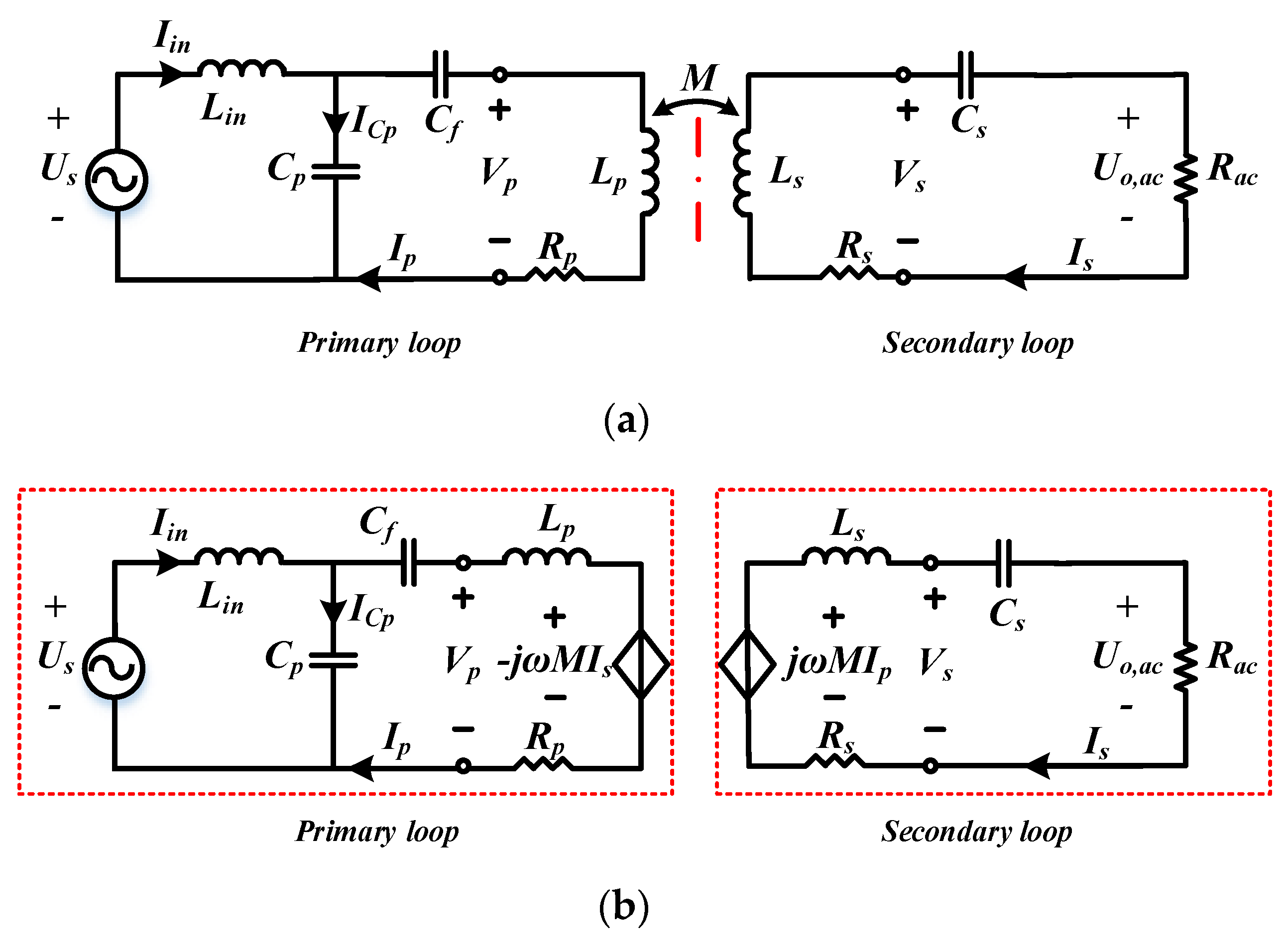
From the previous comparative analysis, it is already possible to recognize the characteristics of S-S and LCCL-S in a tuning situation. However, during the actual charging process, the system often does not operate in the tuning state because of misalignment or deviations in the compensation parameter. Therefore, the comparisons between S-S and LCCL-S topologies in a detuning situation have a greater practical significance. When compared with the compensation parameters of the primary loop, the LCCL-S topology is more sensitive to the compensation parameter variations of the secondary loop [25]. In addition, because S-S and LCCL-S have the same secondary loop structures, for fairness of comparison, only variations in the secondary loop compensation capacitance Cs are considered in this paper.
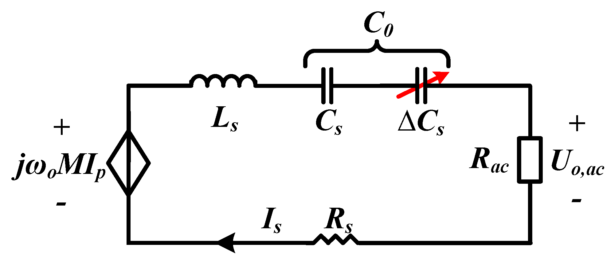
Figure 6 shows the equivalent circuit model of the secondary loop in S-S and LCCL-S compensation topologies in a detuning situation. In Figure 6, oMIp is the equivalent controlled voltage source from the primary loop to the secondary loop. Because the primary loop operates at the ZPA frequency ωo, and the mutual inductance M is nearly constant under the alignment condition, the amplitude of the controlled voltage source is only proportional to the primary current Ip, and the phase is 90° ahead of Ip. Ls is the self-inductance of the secondary coil, and Cs is the resonant compensation capacitance that matches Ls. The relationship can be shown as follows:
j ω o L s + 1 j ω o C s = 0
ΔCs represents the deviation of Cs, and C0 is the equivalent resonant compensation capacitance of the secondary loop under the detuning situation. C0, Cs, and ΔCs satisfy the following relationship:
C 0 = C s + Δ C s
In order to concisely express the effect of the Cs variation on the topology characteristics, a definition is introduced here:
δ = Δ C s C s
Here, δ indicates the degree to which Cs deviates from its original value. If C0 is larger than the standard value Cs, δ is positive. Conversely, if C0 is less than the standard value Cs, δ is negative. In Figure 6, Rs and Rac are the secondary coil resistance and equivalent AC load resistance, respectively, and R0 = Rs + Rac. From (20)–(22), the equivalent impedance of the secondary loop under the detuning situation can be defined as follows:
Z 0 = j ω o L s + 1 j ω o C 0 + R s + R a c = j δ ω o C s ( 1 + δ ) + R 0
Meanwhile, if substituting (23) into (3), the reflection impedance from the primary loop to the secondary loop under the detuning situation can be derived as follows:
Z r 0 = ( ω o M ) 2 Z 0 = ω o 3 M 2 C s ( 1 + δ ) j δ + ω o C s R 0 ( 1 + δ )

3.2.2. Voltage and Current Stresses on Components

In IPT systems, the voltage and current stress on system components is an important index [15]. Excessive stress may cause power losses and affect safe operation. It is difficult to comprehensively compare the stresses of all devices in S-S and LCCL-S because of the different primary circuit structure. However, in this study, the coil parameters of S-S and LCCL-S topologies are identical, furthermore, among the system power losses, the loss caused by the voltage and current stress on the primary and secondary coils is dominant. Thus, a comparison and analysis of the voltage and current stress of coils in S-S and LCCL-S is a reasonable choice under the detuning situation.
Although the system operates under the detuning situation based on the analysis in Section 2, the primary coil current of LCCL-S also remains the same (Ip_LCCL = Us/oLin). The primary coil current of S-S can be obtained by substituting (24) into (4):
I p _ S S = U s R p + Z r 0 = Z 0 U s R p Z 0 + ( ω o M ) 2
Similarly, by substituting (23) into (5) and (13), respectively, the secondary coil currents of S-S and LCCL-S can be derived as follows:
I s _ S S = j ω o M I p _ S S Z 0 = j ω o M U s R p Z 0 + ( ω o M ) 2
I s _ L C C L = j ω o M I p _ L C C L Z 0 = M U s Z 0 L i n
According to the analyses in Section 2, using Kirchhoff’s law and in combination with the above current equations, the voltage of the primary and secondary coils in S-S and LCCL-S compensation topologies can be derived as follows:
V p _ S S = j ω o ( L p I p _ S S M I s _ S S ) = ω o U s ( j Z 0 L p + ω o M 2 ) R p Z 0 + ( ω o M ) 2
V s _ S S = j ω o ( M I p _ S S L s I s _ S S ) = ω o M U s ( j Z 0 + ω o M L s ) R p Z 0 + ( ω o M ) 2
V p _ L C C L = j ω o ( L p I p _ L C C L M I s _ L C C L ) = U s ( Z 0 L p j ω o M 2 ) Z 0 L i n
V s _ L C C L = j ω o ( M I p _ L C C L L s I s _ L C C L ) = M U s ( Z 0 j ω o L s ) Z 0 L i n
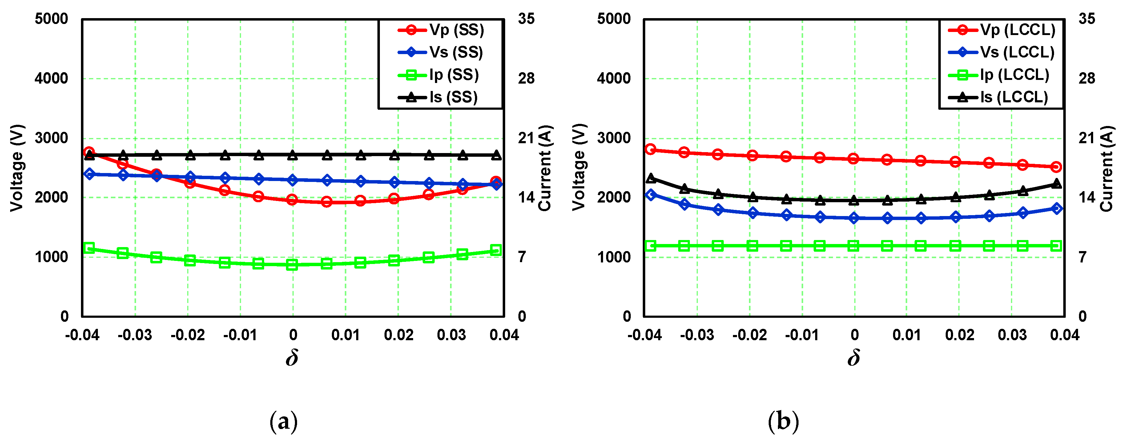
The parameters listed in Table 1 are incorporated into the above voltage and current equations for the calculations. To keep the output power constant (2 kW) when δ varies from −0.04 to 0.04, the calculation results are as shown in Figure 7.
From Figure 7, it can be clearly seen that when the output power is 2 kW under tuning conditions (δ = 0), the values of Vp and Ip of the S-S topology are less than those for the LCCL-S topology. However, the values of Vs and Is of the S-S topology are higher than those for LCCL-S, hence, it is difficult to know which topology incurs a smaller loss in loosely coupled transformers (coils and magnetic pads), and the efficiency comparison of the resonance point requires more analysis and experimental verifications. When δ varies from −0.04 to 0.04 and the output power is fixed at 2 kW, in the primary loop of the S-S topology, Vp and Ip both increase as δ varies. In particular, Vp rises rapidly when δ decreases. However, in the secondary loop, Vs and Is are almost constants, and are independent of δ, and present a constant-power output characteristic. In the LCCL-S topology, according to the previous analysis, Ip remains the same, regardless of variations in δ. Vp shows a slight rise as δ decreases, and decreases slightly as δ increases; these variations are not obvious. However, in the secondary loop, both Vs and Is increase as δ varies, and the growth is approximately symmetrical on both sides of δ = 0. It can be concluded that the voltage and current stress on the primary loop of the LCCL-S topology is more insensitive to variations in δ; however, in the secondary loop, the S-S topology is more stable than the LCCL-S topology under the detuning situation.

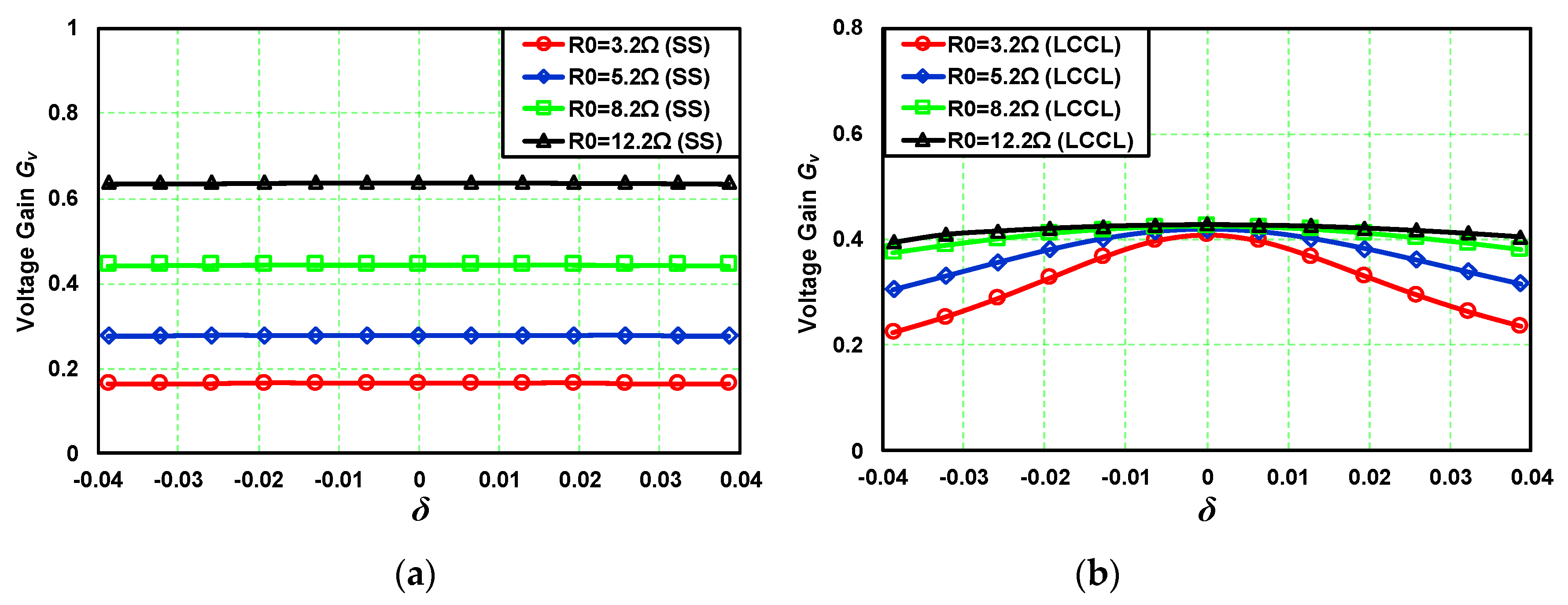
3.2.3. Voltage Gains

As analyzed in Section 2, in IPT systems, a relatively stable output voltage can help to increase efficiency, save cost, and decrease control difficulty. Under tuning conditions, the voltage gains of S-S and LCCL-S are mainly affected by frequency when the system load remains the same. However, under the detuning condition caused by Cs, the operation frequency is fixed at the ZPA frequency, and remains the same. In this section, the influences of the variation in Cs on the voltage gain are analyzed and compared. The voltage gain of S-S topology under the detuning condition can be calculated by substituting (23) into (17):
G v 0 _ S S = | U o , a c _ S S U s | = | j ω M R a c R p Z 0 + ( ω o M ) 2 | = | j ω o 2 C s M R a c ( 1 + δ ) j δ R p + ω o C s ( 1 + δ ) [ R p R 0 + ( ω o M ) 2 ] |  
The voltage gain of the LCCL-S topology under the detuning condition can be calculated by employing (27):
G v 0 _ L C C L = | I s _ L C C L R a c U s | = | M R a c Z 0 L i n | = | ω o M R a c C s ( 1 + δ ) j δ L i n + ω o R 0 C s L i n ( 1 + δ ) |
Using the parameters listed in Table 1, the voltage gains of the S-S and LCCL-S topologies can be calculated by using (32) and (33) when δ changes from -0.04 to 0.04; the calculation results are as shown in Figure 8.
Figure 8 clearly shows that under the premise that the input voltage is fixed at 380 V, in the S-S compensation topology, under the tuning condition (δ = 0), Gv0_SS varies significantly with even small changes in load; this confirms the constant-current source output characteristics of S-S, which is analyzed in Section 2. However, if the loads remain the same, Gv0_SS is a constant that is independent of δ changes. With respect to the voltage gain in the LCCL-S topology, under tuning conditions, Gv0_LCCL is a constant regardless of the load variations. This also confirms the constant-voltage source output characteristics of LCCL-S, which is previously analyzed. However, under the constant-load condition, on both sides of the δ = 0 point, Gv0_LCCL decreases gradually with an increasing deviation of δ. Furthermore, when the load is relatively large, Gv0_LCCL is almost unchanged. As shown in Figure 8b, when R0 = 12.2 Ω, Gv0_LCCL decreased only by 4% in comparison with the tuning point (δ = 0), thus, the LCCL-S topology exhibits an almost constant-voltage source output characteristic under large load conditions. Summarizing the above analysis, under the detuning condition caused by Cs variations, if the load remains the same, the output voltage of the S-S topology is always insensitive to Cs variations in the entire load range. However, with respect to the LCCL-S topology, the output voltage is insensitive to Cs variations, only in the case of large loads.

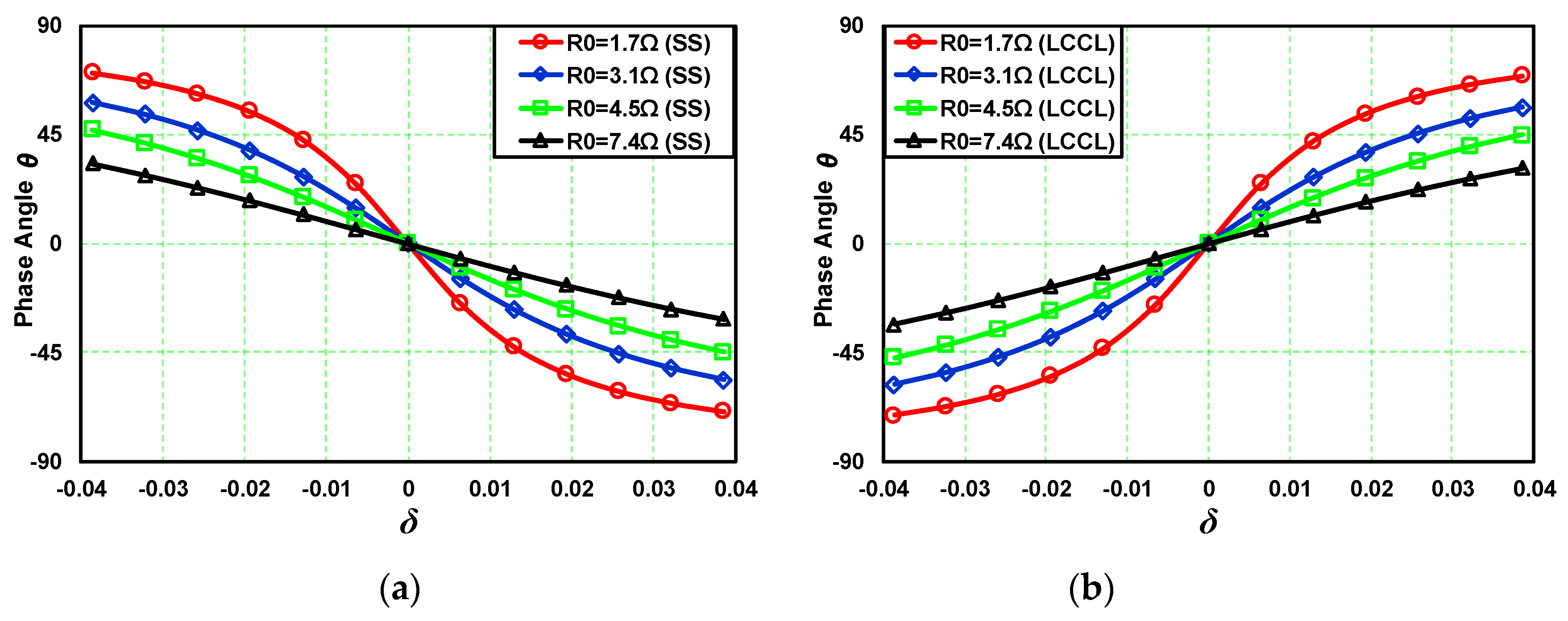
3.2.4. Input Impedances

Similar to the voltage and current stress, the input impedance is closely related to the efficiency and safe operation. As discussed in Section 2, operating under a capacitive input impedance may result in a large switching loss, and may even damage the switch components. Although operating under an inductive input impedance can avoid these problems, an excessive inductive impedance may increase the reactive current and decrease the efficiency. Generally, near the ZPA frequency point, operating under a light inductive impedance can help to obtain the desired efficiency. Under the detuning condition, even if the frequencies, loads, and other parameters remain the same, the variations in Cs may cause the input impedance to be changed.
In the S-S compensation topology, when the primary loop operates at the ZPA frequency and the secondary loop operates in the detuning state caused by Cs variations, according to the previously derived equations, and together with (24), the input impedance of the S-S compensation topology under the detuning condition can be derived as:
Z i n _ S S = Z r 0 + R p = j δ R p + ω o C s ( R p R 0 + ω o 2 M 2 ) ( 1 + δ ) j δ + ω o C s R 0 ( 1 + δ )
By substituting (24) into (11), the input impedance of the LCCL-S compensation topology under the detuning condition can also be derived as:
Z i n _ L C C L = ω o 2 L i n 2 Z r 0 + R p = j δ ( ω o L i n ) 2 + ω o 3 L i n 2 C s R 0 ( 1 + δ ) j δ R p + ω o C s ( R p R 0 + ω o 2 M 2 ) ( 1 + δ )
When δ changes from −0.04 to 0.04, with the parameters listed in Table 1, after substituting (34) and (35) into (19), the phase angle of the input impedances in the S-S and LCCL-S compensation topologies with different loads are as shown in Figure 9.
From Figure 9, it can be clearly seen that, in the S-S compensation topology, when δ is negative (ΔCs < 0), the input impedance from the resistive impedance in δ = 0 to an inductive impedance, when δ is positive (ΔCs > 0), the input impedance from the resistive impedance in δ = 0 to a capacitive impedance. The farther δ deviates from the standard value, the larger is the phase angle. However, this trend is reversed in the LCCL-S compensation topology. The input impedance becomes a capacitive impedance when δ is negative, and becomes an inductive impedance when δ is positive. Similarly, the phase angle increases with the degree of deviation of δ.
According to the previous analysis, during the process of wireless power transfer, a light inductive input impedance can implement ZVS operation; in this way, the switching loss can be reduced and the device safety can be protected. Thus, under the premise of ensuring fairness and for a reasonable comparison, in order to make the following assumptions in subsequent analyses and experiments, in the S-S topology, Cs only varies within the margin for which δ < 0. In the LCCL-S topology, Cs only varies within the margin for which δ > 0. |δ| is used to uniformly indicate the deviation of Cs both in the S-S and LCCL-S compensation topologies.

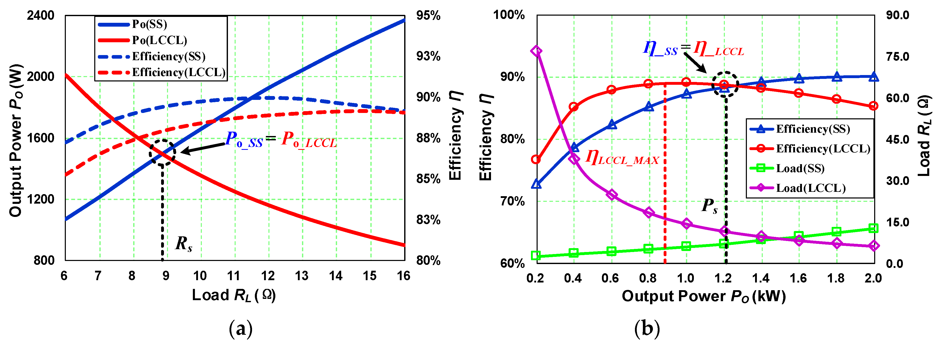
3.2.5. Output Powers

As analyzed in Section 2, under the tuning condition, when the resonance topology parameters of S-S and LCCL-S remain the same, the output power is related only to the loads. The output power of the S-S topology increases as the load increases, but in the LCCL-S topology, the output power increases as the load decreases. According to (26) and (27), under the detuning condition discussed in this paper, the AC output power equations of S-S and LCCL-S can be easily derived as follows:
P o _ S S = | I s _ S S | 2 R a c = ω o 2 M 2 U s 2 R a c | R p Z 0 + ( ω o M ) 2 |
P o _ L C C L = | I s _ L C C L | 2 R a c = M 2 U s 2 R a c | Z 0 | 2 L i n 2
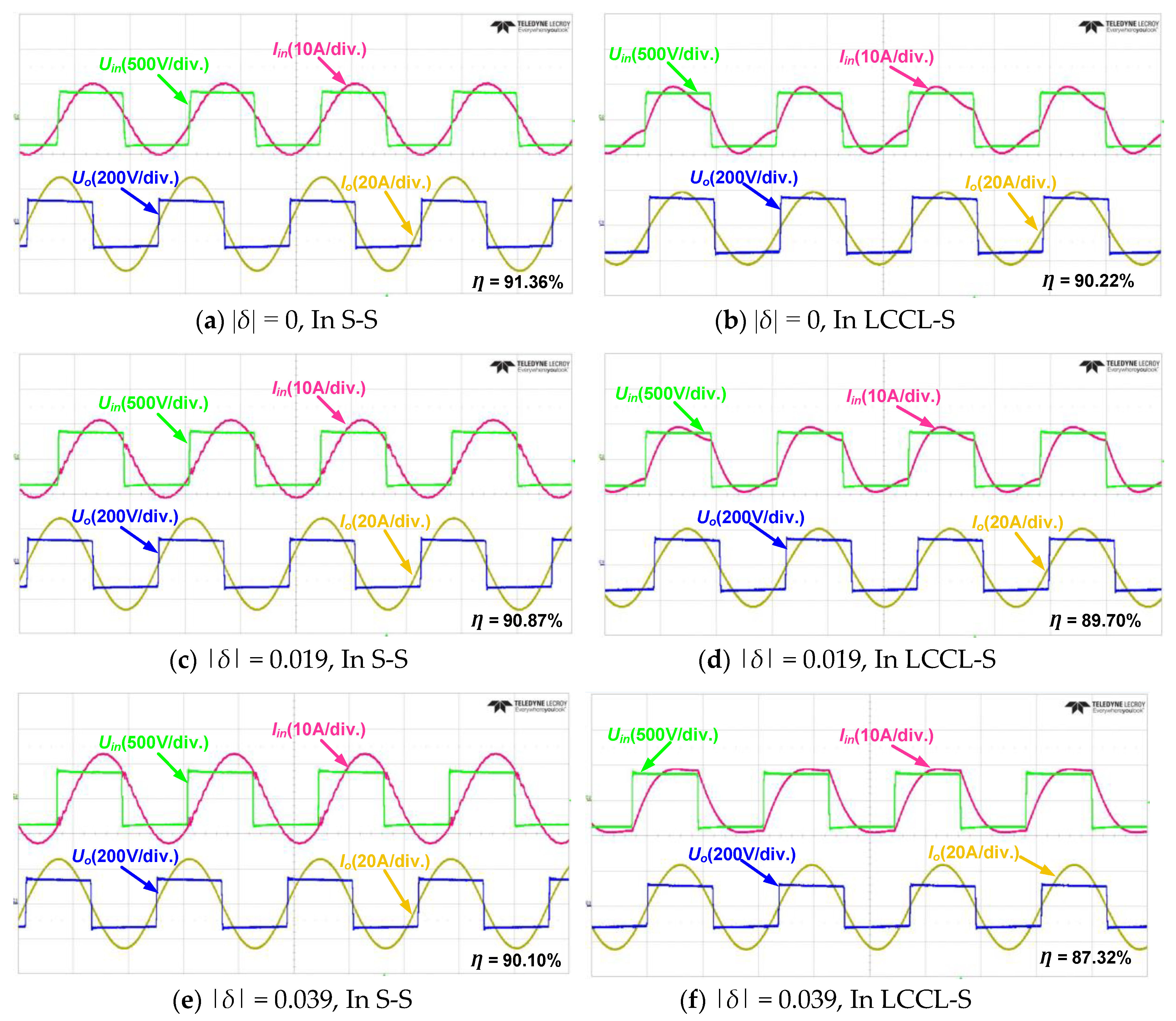
According to the earlier analysis in this section, it can be seen that in the case of constant loads, the output voltage of the S-S topology remains the same, so the output power of the S-S topology is also a constant. However, in the LCCL-S topology, the output voltage decreases as the deviation of Cs increases when the load is small; only under the premise of a large load, the output voltage almost does not vary with variations in Cs. Thus, it can be concluded that for the S-S topology, within the entire power range, the output power does not change with variations in Cs. However, for the LCCL-S topology, the output power decreases with variations in Cs at high-power applications, and is almost unaffected by variations in Cs only in low-power applications.
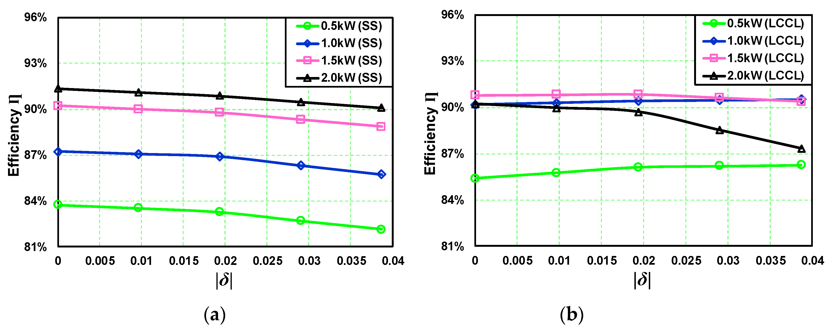
4. Comparative Experiments

4.1. Experimental Setup

In IPT systems, the efficiency is the most important index, and the focus of most related studies has been on improving the efficiency of IPT systems [7,10]. However, owing to the equivalent series resistance (ESR) of the capacitances, iron loss and copper loss of compensation inductances and transmission coils, switching loss, and rectifier loss [15], the efficiency analysis is a complicated task. Furthermore, it is difficult to estimate the efficiency theoretically, and the use of experiments is an effective way of acquiring accurate efficiency data.
In order to compare and analyze the efficiencies of S-S and LCCL-S compensation topologies, a 2.4-kW IPT experimental prototype is configured, and the experimental parameters of the S-S and LCCL-S compensation topologies are the same as the parameters listed in Table 1, The relevant parameters of other experimental equipment are as shown in Table 2, and the 2.4-kW IPT experimental prototype is as shown in Figure 10.

4.2. Comparative Experiment under Tuning Conditons

In order to compare and analyze the efficiency of the S-S and LCCL-S compensation topologies, using the experimental parameters shown in Table 1, comparative experiments under tuning conditions. are performed. The input DC-link voltage is set to 300 V, and the ZPA frequency is designed as 85 kHz. In order to achieve ZVS operation, the operating frequency is set to 85.3 kHz (in S-S) and 84.8 kHz (in LCCL-S). According to the previous analysis, it can be known that the characteristics of the topologies at these frequency points are almost the same as the characteristics of the ZPA frequency points.
Figure 11a shows the comparative experiment results of S-S and LCCL-S under the condition of similar load variations. As the DC load RL increases from 6 Ω to 16 Ω, the output power of S-S (Po_SS) increases and the output power of LCCL-S (Po_LCCL) decreases continuously; the output powers of S-S and LCCL-S are the same (1519 W) at the RL = 8.9 Ω point. Within this load variation range, the efficiency of S-S is always a little higher than the efficiency of LCCL-S; both efficiencies first increase and then decline, and they are almost the same when RL = 16 Ω.
Figure 11b shows the comparative experimental results of S-S and LCCL-S in the case involving similar power variations. When the output powers of S-S and LCCL-S increase from 200 W to 2000 W, the efficiency of LCCL-S (Ƞ_LCCL) increases first and then declines; it reaches a maximum (89.24%) when the output power is 910 W. However, within the same range of output power variations, the efficiency of S-S (Ƞ_SS) increases continuously, and it increases rapidly in the low-power range. The rate of increase of the efficiency dropped significantly after 1400 W, and the maximum efficiency is 91.34% when Po = 2000 W. At the point of Ps = 1278 W, there is Ƞ_LCCL = Ƞ_SS (88.58%). The efficiency of LCCL-S is higher when Po < Ps, and the efficiency of S-S is higher when Po > Ps. It can also be seen from Figure 11b that as Po varies from 200 W to 2000 W, the load variation range of LCCL-S is 6.07 Ω–77 Ω. However, the load variation range of S-S is only 2.4 Ω–12.5 Ω, the output power of S-S is more sensitive to the load variation than LCCL-S under tuning conditions.

4.3. Comparative Experiment under Detuning Conditions

In order to compare and analyze the efficiencies of S-S and LCCL-S under detuning conditions, a comparative experiment is performed with variations in Cs. The experimental parameters are consistent with Table 1, and the standard Cs value that corresponds to |δ| = 0 is 15.51 nF. According to the instructions in Section 3.2.4, the Cs value of S-S is decreased from 15.51 nF, and that of LCCL-S is increased from 15.51 nF, giving the same deviation of Cs to make the two topologies operate at the ZVS region. It also uses |δ| to indicate the same deviation of Cs in S-S and LCCL-S. As |δ| changes from 0–0.39, comparative experiments are performed when the output power values are 0.5 kW, 1 kW, 1.5 kW, and 2 kW. In each set of comparative experiments, the output power is kept constant by slightly adjusting the loads. The efficiency variations in each set were measured.
Figure 12 shows the efficiencies of S-S and LCCL-S when |δ| varies from 0–0.39. It can be seen from Figure 12a that at different output power levels (0.5 kW–2 kW), the efficiencies of the S-S topology all continuously decrease with the increase of |δ|. However, in the S-S topology, as the output power increases, there is a slower decreasing trend of the efficiencies. As |δ| increases from 0–0.39, the total efficiency decreases by 1.61% when the output power is 0.5 kW, and it decreased by 1.26% when the output power is 2 kW. Figure 13a,c,e show the input and output AC voltage and current waveforms of the S-S topology at different values of |δ| when the output power is 2 kW; when other parameters and the output power remain the same, with the increase in |δ|, the phase angle of the input impedance increases rapidly; thus, the power factor (PF) of the input voltage and current decreases. The output voltage and current are almost unchanged, and the power loss of the secondary loop in the S-S topology is therefore constant, and is independent with the increase of |δ|. Although the input current shows a slight increase, the increase in the loss is not obvious in the primary loop of the S-S topology with fewer power devices. Hence, as the power increases, the ratio of the power increase is much greater than the increase in the loss, even if the deviation |δ| is obvious. S-S still has a high efficiency in high-power applications.
From Figure 12b, it can be found that for the LCCL-S topology, in the case of a low output power, such as 0.5-kW and 1-kW curves shown in Figure 12b, although the efficiencies increase as |δ| increases, the increase trend is not obvious. When |δ| increases from 0–0.39, the total efficiency increased by 0.868% when the output power is 0.5 kW, and it increased by 0.343% when the output power is 1 kW. However, in the case of a high output power, similar to the S-S topology, the efficiencies of LCCL-S decrease as the |δ| increase. Although the efficiency only decreased by 0.4% at the 1.5-kW point, when the output power is 2 kW, the efficiency suddenly decreased by 2.9%. As the output power increases, the decreasing trend of the efficiency may continue to increase. The result waveforms of LCCL-S under the condition of |δ| variations when the output power is 2 kW are as shown in Figure 13b,d,f.
With the increase of |δ|, the phase angle of the input impedance also increased rapidly, and the PF decreases. The input current increases slightly, but the waveforms fluctuate significantly. According to the previous analysis that the current of the primary coil is constant, the loss of the primary loop in LCCL-S is relatively stable. However, in the secondary loop, the output voltage drops dramatically with the increase of |δ|. Therefore, under the premise of keeping the same output power, the output current needs to be significantly improved, so the loss of the secondary loop in LCCL-S is increased as the |δ| increase, especially in high-power applications.

5. Conclusions

In this study, the electrical characteristics of S-S and LCCL-S compensation topologies are analyzed and compared in both tuning and detuning states. In particular, under the detuning conditions caused by Cs variations, the voltage and current stresses on components, input impedances, voltage gains, and output powers are analyzed and compared using δ. A 2.4-kW experimental prototype is configured to obtain an efficiency comparison between S-S and LCCL-S topologies. According to the comparative results, it can be concluded that in the tuning state, S-S presents a constant-current source characteristic to the load, and the maximum efficiency is achieved under the high-output-power condition. However, LCCL-S presents a constant-voltage source characteristic to the load, and the maximum efficiency is achieved under the low-output-power condition. The output characteristic of S-S is more sensitive to load variations than LCCL-S. In the detuning state, under the premise that the remaining parameters are the same and that only Cs, changes, the output characteristic of S-S is almost not affected by the variations of Cs within the entire load range. Although the efficiency of S-S decreases with the deviation of Cs, the downtrend is not obvious in high-power situations. However, in the LCCL-S topology, the output characteristic of LCCL-S is not affected by the variations of Cs only in low-output-power (light load) situations. The efficiency of LCCL-S decreases rapidly in high-power situations. S-S is less sensitive to Cs variations than LCCL-S in high-power applications. In conclusion, S-S is more suitable in high-power EV applications and LCCL-S is more suitable in low-power EV applications. The presented analysis method in this study also can be adopted to other applications such as mobile phones and unmanned aerial vehicles (UAVs).

Author Contributions

Conceptualization, Y.C., H.Z. and D.-H.K.; Data curation, Y.C. and H.Z.; Formal analysis, Y.C. and H.Z.; Funding acquisition, D.-H.K.; Investigation, Y.C. and S.-J.P.; Project administration, D.-H.K.; Writing—original draft, Y.C.; Writing—review & editing, D.-H.K.

Funding

This research was supported by Korea Electric Power Corporation (Grant number: R18XA04) and the National Research Foundation of Korea (NRF) grant funded by the Korea government (MSIT) (No. NRF-2017R1C1B2010057).

Conflicts of Interest

The authors declare no conflicts of interest.

Nomenclature

UsEquivalent AC input voltage of the IPT system
UDCDC-link voltage of IPT system
nThe Fourier odd harmonic label of Us
φFrequency corresponding angle of Us
RacEquivalent AC load resistance
RpEquivalent resistance of the primary loop
RsEquivalent resistance of the secondary loop
LpSelf-inductance of the primary coil
LsSelf-inductance of the secondary coil
ZpEquivalent impedance of the primary loop
ZsEquivalent impedance of the secondary loop
ZinEquivalent input impedance of the IPT system
ZrReflection impedance of the secondary loop
ωOperation frequency of the IPT system
ωoZero phase angle frequency of the IPT system
kCoupling coefficient
MMutual inductance of the coils
Uo,acEquivalent AC output voltage of the IPT system
GvVoltage gain of the IPT system
θinInput impedance angles of the IPT system
C0Equivalent resonant compensation capacitance of the secondary loop under the detuning situation
ΔCsDeviation of the secondary compensation capacitance
δIndex of secondary compensation capacitance deviation

References

  1. Patil, D.; McDonough, M.K.; Miller, J.M.; Fahimi, B.; Balsara, P.T. Wireless power transfer for vehicular applications: Overview and challenges. IEEE Trans. Transp. Electrif. 2018, 4, 3–37. [Google Scholar] [CrossRef]
  2. Kim, S.; Covic, G.A.; Boys, J.T. Tripolar pad for inductive power transfer systems for EV charging. IEEE Trans. Power Electron. 2017, 32, 5045–5057. [Google Scholar] [CrossRef]
  3. Bosshard, R.; Kolar, J.W. Inductive power transfer for electric vehicle charging: Technical challenges and tradeoffs. IEEE Power Electron. Mag. 2016, 3, 22–30. [Google Scholar] [CrossRef]
  4. Mai, R.; Lu, L.; Li, Y.; He, Z. Dynamic Resonant Compensation Approach Based on Minimum Voltage and Maximum Current Tracking for IPT System. Trans. China Electrotech. Soc. 2015, 30, 32–38. [Google Scholar]
  5. Madawala, U.K.; Thrimawithana, D.J. A bidirectional inductive power interface for electric vehicles in V2G systems. IEEE Trans. Ind. Electron. 2011, 58, 4789–4796. [Google Scholar] [CrossRef]
  6. Covic, G.A.; Boys, J.T. Modern trends in inductive power transfer for transportation applications. IEEE J. Emerg. Sel. Top. Power Electron. 2013, 1, 28–41. [Google Scholar] [CrossRef]
  7. Del Toro, T.G.X.; Vázquez, J.; Roncero-Sanchez, P. Design, implementation issues and performance of an inductive power transfer system for electric vehicle chargers with series-series compensation. IET Power Electron. 2015, 8, 1920–1930. [Google Scholar]
  8. Li, S.; Mi, C.C. Wireless Power Transfer for Electric Vehicle Applications. IEEE J. Emerg. Sel. Top. Power Electron. 2015, 3, 4–17. [Google Scholar]
  9. Villa, J.L.; Sallan, J.; Sanz Osorio, J.F.; Llombart, A. High-Misalignment Tolerant Compensation Topology for ICPT Systems. IEEE Trans. Ind. Electron. 2012, 59, 945–951. [Google Scholar] [CrossRef]
  10. Zhang, W.; Mi, C. Compensation Topologies of High Power Wireless Power Transfer Systems. IEEE Trans. Veh. Technol. 2016, 65, 4768–4778. [Google Scholar] [CrossRef]
  11. Kan, T.Z.; Nguyen, T.D.; White, J.C.; Malhan, R.K.; Mi, C.T. A New Integration Method for an Electric Vehicle Wireless Charging System Using LCC Compensation Topology: Analysis and Design. IEEE Trans. Power Electron. 2017, 32, 1638–1650. [Google Scholar] [CrossRef]
  12. Wang, Y.; Yao, Y.; Liu, X.; Xu, D. S/CLC compensation topology analysis and circular coil design for wireless power transfer. IEEE Trans. Transp. Electrif. 2017, 3, 496–507. [Google Scholar] [CrossRef]
  13. Kim, M.; Joo, D.M.; Woo, D.G.; Lee, B.K. Design and control of inductive power transfer system for electric vehicles considering wide variation of output voltage and coupling coefficient. In Proceedings of the 2017 IEEE Applied Power Electronics Conference and Exposition (APEC), Tampa, FL, USA, 26–30 March 2017. [Google Scholar]
  14. Ali, R.; Shahrokh, F.; Hossein, I.E.; Babak, F.; Ramin, R.; Gholam, R.M. Optimized LCC-Series Compensated Resonant Network for Stationary Wireless EV Chargers. IEEE Trans. Ind. Electron. 2019, 66, 2756–2765. [Google Scholar]
  15. Li, W.; Zhao, H.; Deng, J.; Li, S.; Mi, C.C. Comparison Study on SS and double-sided LCC compensation topologies for EV/PHEV Wireless Chargers. IEEE Trans. Veh. Technol. 2016, 65, 4429–4439. [Google Scholar] [CrossRef]
  16. Esteban, B.; Sid-Ahmed, M.; Kar, N.C. A Comparative Study of Power Supply Architectures in Wireless EV Charging Systems. IEEE Trans. Power Electron. 2015, 30, 6408–6422. [Google Scholar] [CrossRef]
  17. Konrad, W.; Alireza, S. A practical approach to inductive power transfer systems for transportation applications using boucherot bridge method. In Proceedings of the 2014 IEEE Transportation Electrification Conference and Expo (ITEC), Dearborn, MI, USA, 15–18 June 2014. [Google Scholar]
  18. Mai, R.; Yue, P.; Liu, Y.; Zhang, Y.; He, Z. A Dynamic Tuning Method Utilizing Inductor Paralleled with Load for Inductive Power Transfer. IEEE Trans. Power Electron. 2018, 33, 10924–10934. [Google Scholar] [CrossRef]
  19. William, J.W.; Hu, A.P.; Swain, A. A Wireless Power Pickup Based on Directional Tuning Control of Magnetic Amplifier. IEEE Trans. Ind. Electron. 2009, 56, 2771–2781. [Google Scholar]
  20. Igarashi, H. Semi-analytical approach for finite-element analysis of multi-turn coil considering skin and proximity effects. IEEE Trans. Power Magn. 2016, 53, 1–7. [Google Scholar] [CrossRef]
  21. Steigerwald, R.L. A comparison of half-bridge resonant converter topologies. IEEE Trans. Power Electron. 1988, 3, 174–182. [Google Scholar] [CrossRef]
  22. Zhao, L.; Thrimawithana, D.J.; Madawala, U.K. Hybrid Bidirectional Wireless EV Charging System Tolerant to Pad Misalignment. IEEE Trans. Ind. Electron. 2017, 64, 7079–7086. [Google Scholar] [CrossRef]
  23. Zhang, W.; Wong, S.C.; Tse, C.K. Design for Efficiency Optimization and Voltage Controllability of Series–Series Compensated Inductive Power Transfer Systems. IEEE Trans. Power Electron. 2014, 29, 191–200. [Google Scholar] [CrossRef]
  24. Byeon, J.; Kang, M.; Kim, M.; Joo, D.M.; Lee, B.K. Hybrid control of inductive power transfer charger for electric vehicles using LCCL-S resonant network in limited operating frequency range. In Proceedings of the 2016 IEEE Energy Conversion Congress and Exposition (ECCE), Milwaukee, WI, USA, 18–22 September 2016. [Google Scholar]
  25. Zhou, S.; Mi, C.C. Multi-Paralleled LCC Reactive Power Compensation Networks and Their Tuning Method for Electric Vehicle Dynamic Wireless Charging. IEEE Trans. Ind. Electron. 2016, 63, 6546–6556. [Google Scholar] [CrossRef]
Figure 1. Schematic of the IPT system for EVs.
Energies 12 01913 g001
Figure 2. Circuit analysis model of S-S. (a) Mutual inductive topology model; (b) Decoupling independent voltage source model.
Energies 12 01913 g002
Figure 3. Circuit analysis model of LCCL-S. (a) Mutual inductive topology model; (b) Decoupling independent voltage source model.
Energies 12 01913 g003
Figure 4. Equivalent circuit of primary loop in LCCL-S.
Energies 12 01913 g004
Figure 5. Bode diagrams of S-S and LCCL-S compensation topologies. (a) Amplitude-frequency characteristic of S-S; (b) Phase-frequency characteristic of S-S; (c) Amplitude-frequency characteristic of LCCL-S; (d) Phase-frequency characteristic of LCCL-S.
Energies 12 01913 g005
Figure 6. Equivalent detuning circuit model of secondary loop in S-S and LCCL-S compensation topologies.
Energies 12 01913 g006
Figure 7. Under the condition of δ variations, the voltage and current stresses (RMS values) on both coils in S-S and LCCL-S compensation topologies when output power is fixed at 2 kW. (a) In S-S topology; (b) In LCCL-S topology.
Energies 12 01913 g007
Figure 8. Graph showing variations in δ, the voltage gains of the S-S and LCCL-S compensation topologies in the case of load variations. (a) In the S-S topology; (b) In the LCCL-S topology.
Energies 12 01913 g008
Figure 9. Under the condition of varying δ, the phase angle of the input impedances in S-S and the LCCL-S compensation topologies in the case of load variations. (a) In S-S topology; (b) In LCCL-S topology.
Energies 12 01913 g009
Figure 10. 2.4-kW IPT experimental prototype. (a) Compensation devices; (b) Main instruments.
Energies 12 01913 g010
Figure 11. Comparative experiment results of S-S and LCCL-S compensation topologies under tuning condition. (a) Load variation experiment; (b) Output power variation experiment.
Energies 12 01913 g011
Figure 12. Comparative experiment results of S-S and LCCL-S compensation topologies under detuning condition. (a) Efficiency of S-S topology; (b) Efficiency of LCCL-S topology.
Energies 12 01913 g012
Figure 13. Experimental waveforms of S-S and LCCL-S compensation topologies under detuning condition when output power is 2 kW.
Energies 12 01913 g013
Table 1. Specifications and parameters of the IPT system.
NoteSymbol Value
DC-link voltageUDC380 V
ZPA frequencyfo85 kHz
Coupling coefficientk0.0916 1
Primary coil self-inductanceLp595.37 μH 1
Secondary coil self-inductanceLs226.22 μH 1
Primary coil resistanceRp0.13 Ω 1
Secondary coil resistanceRs0.18 Ω 1
Primary loop compensation inductanceLin77.42 μH 1
Primary loop series compensation capacitance (S-S)Cp5.89 nF 1
Primary loop shunt compensation capacitance (LCCL-S)Cp45.33 nF 1
Primary loop series compensation capacitanceCf6.78 nF 1
Secondary loop series compensation capacitanceCs15.51 nF 1
1 Actually measured parameter values.
Table 2. Specifications of the experimental setup.
ParameterDescription
Digital signal processorTMS320F28335
MOSFETs of FB inverter(S1–S4)IPW60R075CP (650 V/39 A)
Diodes of rectifier (D1–D4)IDW20G120C5B(1200 V/20 A)
DC power supplyKEYSIGHT N8955A (15,000 W)
Power analyzerHIOKI PW6001(1500 V/50 kA)
DC electronic loadChroma 63205A-600-350 (5 kW)

