Article

ZVS Auxiliary Circuit for a 10 kW Unregulated LLC Full-Bridge Operating at Resonant Frequency for Aircraft Application

1
Centro de Electrónica Industrial, Universidad Politécnica de Madrid, Madrid 28006, Spain
2
Indra Sistemas, S.A., Indra Sistemas, Calle de Joaquín Rodrigo, 11, 28300 Aranjuez, Madrid, Spain
*
Author to whom correspondence should be addressed.
Energies 2019, 12(10), 1850; https://doi.org/10.3390/en12101850
Submission received: 12 April 2019 / Revised: 10 May 2019 / Accepted: 13 May 2019 / Published: 15 May 2019
(This article belongs to the Special Issue Advances in High-Efficiency LLC Resonant Converters)

Abstract

:
In modern aircraft designs, following the More Electrical Aircraft (MEA) philosophy, there is a growing need for new high-power converters. In this context, innovative solutions to provide high efficiency and power density are required. This paper proposes an unregulated LLC full-bridge operating at resonant frequency to obtain a constant gain at all loads. The first harmonic approximation (FHA) model is not accurate enough to estimate the voltage gain in converters with high parasitic resistance. A modified FHA model is proposed for voltage gain analysis, and time-based models are used to calculate the instantaneous current required for the ZVS transition analysis. A method using charge instead of current is proposed and used for this ZVS analysis. Using this method, an auxiliary circuit is proposed to achieve complete ZVS within the whole load range, avoiding a gapped transformer design and increasing the efficiency and power density. A 28 Vdc output voltage prototype, with 10 kW peak output power, has been developed to validate the theoretical analysis and the proposed auxiliary circuit. The maximum efficiency (96.3%) is achieved at the nominal power of 5 kW.

1. Introduction

In the field of the More Electrical Aircraft (MEA) philosophy, there is a tendency to substitute mechanical, hydraulic and pneumatic systems with their electrical equivalents in order to increase efficiency and reduce cost and fuel consumption [1,2,3]. As a result, the electrical power demand of modern aircraft has increased and new power conversion solutions are needed.
Aircraft generators typically supply electrical power in AC at variable frequency (360 Hz/800 Hz; see Figure 1); however, aircraft loads require 28 Vdc [4]. Traditional aircraft rectifiers are based on passive solutions, with low-frequency transformers and diode rectifications. This approach is very robust, but the power density is low and offers limited regulation capabilities. Following the MEA philosophy, active rectifier solutions are being developed. These active solutions can be more efficient, with an optimized volume and weight, and can also reduce the harmonic content in the AC grid, which increases the lifecycle of the generators. Active aircraft rectifier systems are typically composed of three stages, as shown in Figure 1: an EMI filter, AC/DC rectifier and isolated DC/DC converter.
This article will focus on the DC/DC stage following the specifications in Table 1; a previous publication on the design can be found in [5]. Additional information on the rectifier stage can be found in [6]. The output voltage is fed and controlled by the rectifier, as depicted in Figure 1. Therefore, the DC/DC converter needs a constant gain ( K = 1 / 14 ) for all loads.
For a high-power isolated converter, full-bridge based topologies are known to be the most adequate solution in terms of volume and losses [7]. High-frequency operation is desirable to decrease the magnetic component volume and weight; however, switching losses in the devices will increase. That is why soft-switched topologies offer a good trade-off between efficiency and volume, such as with LLC converters, which are widely used in different applications [8,9].
The topology selected for this application is the LLC full-bridge operating at resonant frequency [10,11,12], at which the maximum efficiency is reached. However, this operation point is at the crossroad between zero voltage switching (ZVS) and zero current switching (ZCS) for primary devices. ZCS and ZVS are mutually exclusive soft switching techniques and, in high-current converters, ZCS achieves a higher loss reduction than ZVS. However, aircraft noise standards are restrictive. Therefore, ZVS operation must be achieved in high-voltage converters to avoid voltage spikes and ensure robust operation and low emitted noise. The ZVS capabilities within the whole load range have been analyzed extensively in the literature [13,14]. However, since operation at resonant frequency is between the ZCS and ZVS regions, time-based (TB) simulations are needed to estimate the range of ZVS depending on different LLC design parameters. Additionally, in LLC converters, the current is not constant along the ZVS transition and must be analyzed in terms of charge rather than current using time-based models. This is not considered in previous publications.
To achieve complete ZVS within the whole load range in unregulated LLC converters, the design leads to high circulating currents and a gapped transformer. However, auxiliary circuits can be used to increase the ZVS range in full-bridge converters; some are active [15] and others are passive [16,17,18], and they consist typically of two inductive circuits connected to the middle point of each leg. This work proposes a new configuration for the ZVS auxiliary circuit, specific to LLC full-bridge topology, with a single inductor connected between both middle points, reducing the circuit to a single inductor. With this circuit, ZVS can be achieved for the whole load range with an optimized transformer design without gaps and with LLC parameters optimized to reduce circulating currents.
First harmonic approximation (FHA) is an analytical method to estimate the voltage gain in resonant converters [19]. There are modifications of the FHA method in the literature, to account for higher harmonics [20,21]. However, these methods do not consider load-dependent behavior. In regulated LLC converters, the control loop can compensate for the error in gain. In unregulated LLC converters, an accurate estimation of the voltage gain mismatch is required. The unregulated LLC converter in this work has an external control loop to compensate the voltage gain error. However, an accurate voltage gain is required to estimate the components maximum voltage for the DC/DC and AC/DC stages from Figure 1.
Two modified FHA methods for voltage gain estimation are proposed in this paper and compared with their time-based equivalents. The first method includes a series resistance to account for the load-dependent voltage drop and the second method includes the distributed impedance model of the transformer.
Using the ZVS analysis and the modified FHA method, this work proposes an unregulated LLC full-bridge operating at resonant frequency with an auxiliary circuit to achieve complete ZVS within the whole load range. A 10 kW prototype is constructed to validate the topology and the models.

2. LLC Full-Bridge Topology: Operation Principle and Accurate Modeling

In this article, the considered topology is an unregulated LLC full-bridge with full-bridge rectifier, as shown in Figure 2. The duty cycle is constant and close to 50%, allowing a constant dead-time to achieve the ZVS transitions.
Normalization is performed with the parameters defined in Table 2.
In Table 2, f s is the switching frequency and f r is the resonant frequency of the series tank, and R O * is the reflected load AC-equivalent resistance for the output full-bridge rectifier. The rest of the parameters are defined in Figure 2.
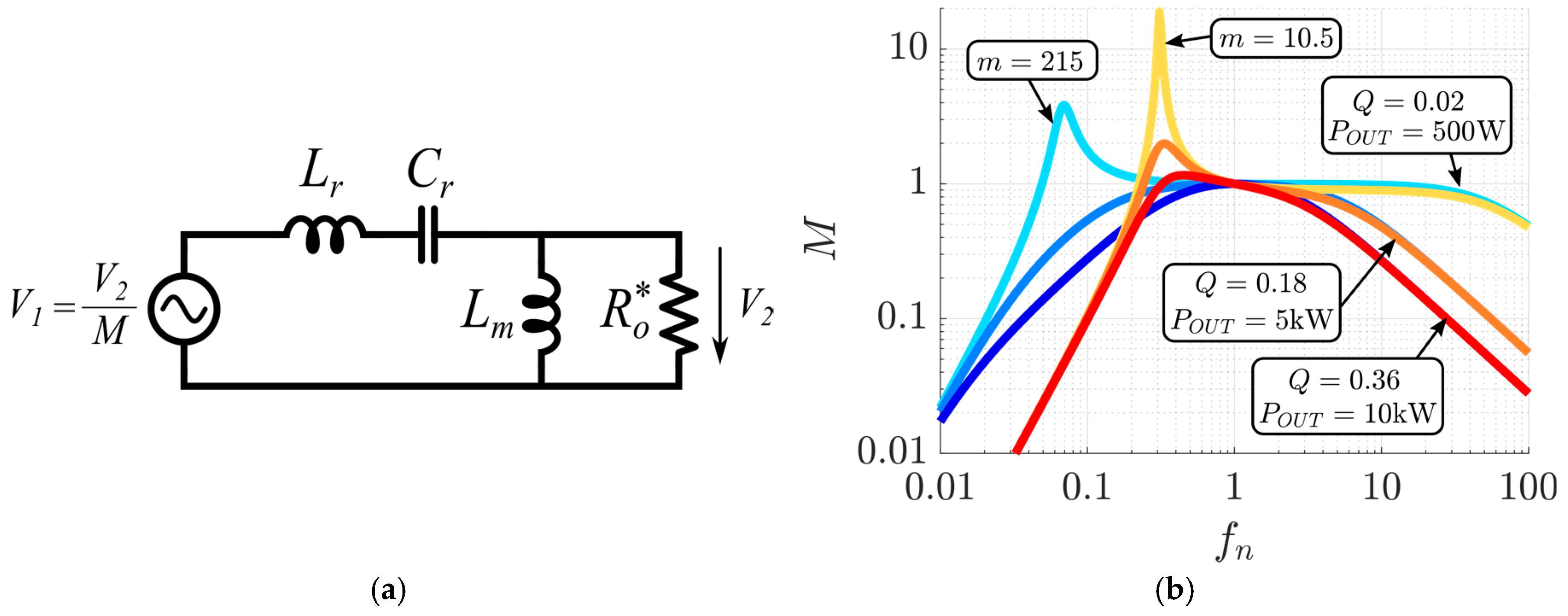
The analytical equation for the gain is derived from the equivalent circuit shown in Figure 3a using the conventional first harmonic approximation (FHA) [19]:
M = V 2 V 1 = n · V O U T V I N = 1 ( 1 + 1 m 1 ( 1 1 f n 2 ) ) 2 + Q 2 ( f n 1 f n ) 2
Figure 3b shows the gain ( M ) at different quality factors ( Q ) and inductance ratios ( m ) within a range of normalized frequencies ( 0.5 < f n < 2 ).
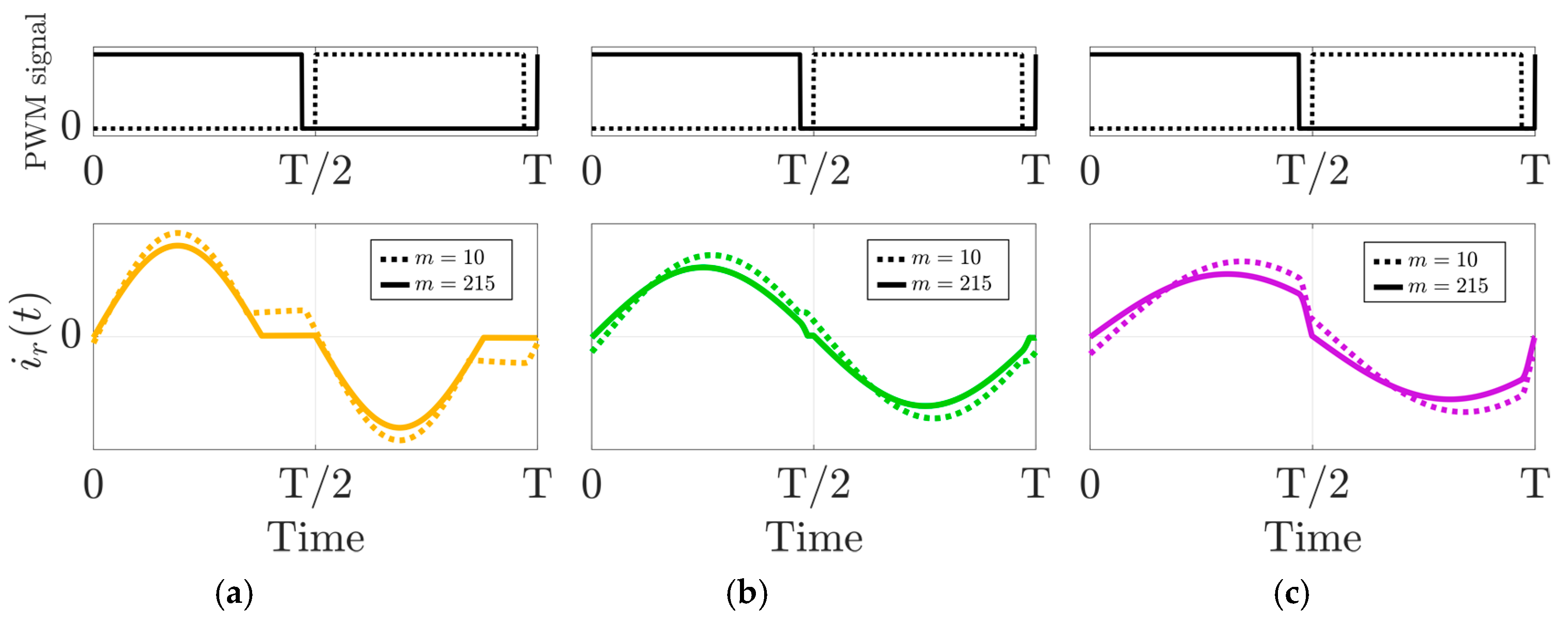
Three different modes can be defined for the operation of the LLC converter: below resonance ( f n < 1 ), at resonance ( f n = 1 ) and above resonance ( f n > 1 ). The current shapes of each mode are shown in Figure 4 at two different inductance ratios ( m ).

2.1. Unregulated LLC Optimum Design and Power Loss Model

In regulated LLC converters, the minimum and maximum operating frequencies are selected to achieve the desired voltage gain. However, in unregulated LLC converters, to achieve a constant gain at all loads, the frequency is kept constant. A constant gain is only possible when operating at resonant frequency. Additionally, operation at resonant frequency achieves the best trade-off of power losses, as depicted in Figure 5. The model used for the MOSFET power loss can be found in the Infineon application note [22]. The conduction losses for a full-bridge configuration of MOSFET are calculated with the following equation:
P C = 4 R D S o n ( 100   ° C ) N M O S I R M S _ M 2
where R D S o n ( 100   ° C ) is the drain-source resistance of the MOSFET with a junction temperature of 100 °C as a worst case, N M O S is the number of devices in parallel for a switch position, and I R M S _ M is the switch total RMS current:
P s = f s N M O S V D S M A X ( I D O N t r i + t f u 2 + Q r r + I D O F F t r u + t f i 2 ) ,
where V D S M A X is V I N for primary-side and V O U T for secondary-side devices, I D O N and I D O F F are the turn-on and turn-off drain currents, t r i , t f u , t r u , t f i are the rise and fall times of current and voltage, respectively, and finally Q r r is the reverse recovery charge.
To calculate the winding losses, the following equation is used:
P w i n d i n g = R A C ( 100   kHz )   I R M S T 2
where I R M S _ T is the transformer RMS current and R A C ( 100   kHz ) is the AC resistance of the winding estimated using FEA analysis, using Pemag–Maxwell.
Finally, the core losses are estimated using the improved generalized Steinmetz equation (iGSE) [23]:
P c o r e = 1 T 0 T k i | d B d t | α ( Δ B ) β α d t
where B is the flux in the core, α , β are the Steinmetz coefficients, and k i is the improved Steinmetz coefficient. The components used can be found in Table 6 in Section 5. To summarize the total losses from breakdown in Figure 5 and Figure 6, the losses are merged into three main categories of conduction losses,
P C o n d = P C 1 + P C 2 + P w i n d i n g + P P a r a s i t i c s ,
consisting of the sum of the transistor conduction losses from primary and secondary sources, the winding losses of the transformer and the conduction losses of the parasitic resistances across the converter. Then, the switching losses consist of the sum of primary and secondary transistor switching losses, using Equation (3), and the core losses using Equation (5).
In Figure 5, for high inductance ratios ( m ), minimum losses are not reached at f n = 1 but at f n = 1 t d · f r , where complete ZCS is achieved. When comparing the behavior between high and low inductance ratios with the LLC converter, we can see in Figure 5a,b that m = 215 has lower power losses. This is caused by the high circulating currents and high turn-off currents of the m = 10 case.
These high circulating currents can be noticed at low load, as depicted in Figure 6, where the conduction losses are negligible for m = 215 but are considerable for m = 10 .
The voltage gain is M = 1 , when neglecting the load-dependent voltage drop and the effects of undesired parasitic elements. These effects are usually neglected in regulated LLC converters, because the feedback loop adjusts the voltage gain to the desired value. However, in unregulated LLC converters, the frequency is constant and the gain varies as a function of the load. In the system depicted in Figure 1, the DC/DC stage input voltage will be adjusted by the AC/DC stage. However, the input voltage range is required for the design of the AC/DC stage.
Because the converter is unregulated, the resonant frequency of the tank changes with the component value drift. If the switching frequency is not changed to match the new resonant frequency, the converter will not operate at the optimum efficiency. This issue can be solved by measuring the input and output voltage and implementing an algorithm to search for the maximum gain, which will also be the point of maximum efficiency. This is not a control loop, and it can be performed only once during the startup process. As explained before, the voltage gain varies with the output load and the conventional FHA does not consider this load influence and other parasitics. Therefore, more accurate modified models are needed to design unregulated LLC converters.
The next sections describe two FHA models with modified circuits with different parasitic elements added.

2.2. FHA and TB Models Considering the Series Resistance

As discussed previously, the effect of the load-dependent voltage drop cannot be neglected to estimate the gain. To consider this effect, series resistance is added to the equivalent circuit in in Figure 3a, as shown in Figure 7. The modified FHA model in Figure 7a is compared to the time-based (TB) model of Figure 7b. The addition of the resistance dampens the series resonance of the LLC tank, so higher harmonics are introduced in the current and non-linearities are no longer negligible. Therefore, the conventional FHA circuit is not accurate when the harmonic content is high.
The analytical equation for the gain is derived from the modified FHA circuit, as illustrated in Figure 7a:
M = 1 ( 1 + 1 ( m 1 ) ( 1 1 f n 2 ) Q Q s ) 2 + Q 2 · ( f n 1 f n 1 f n 2 · ( 1 ( m 1 ) Q Q s ) ) 2  
This equation is the same as Equation (1) with additional terms in bold. These terms contain a new parameter, the quality factor of the series resonant tank, which is defined as follows:
Q s = 1 R s L r C r
This parameter includes the series resistance R s , as depicted in Figure 7. It consists of all the resistances in series between the primary and secondary voltage bridges, including the resistances of the primary and secondary switches.
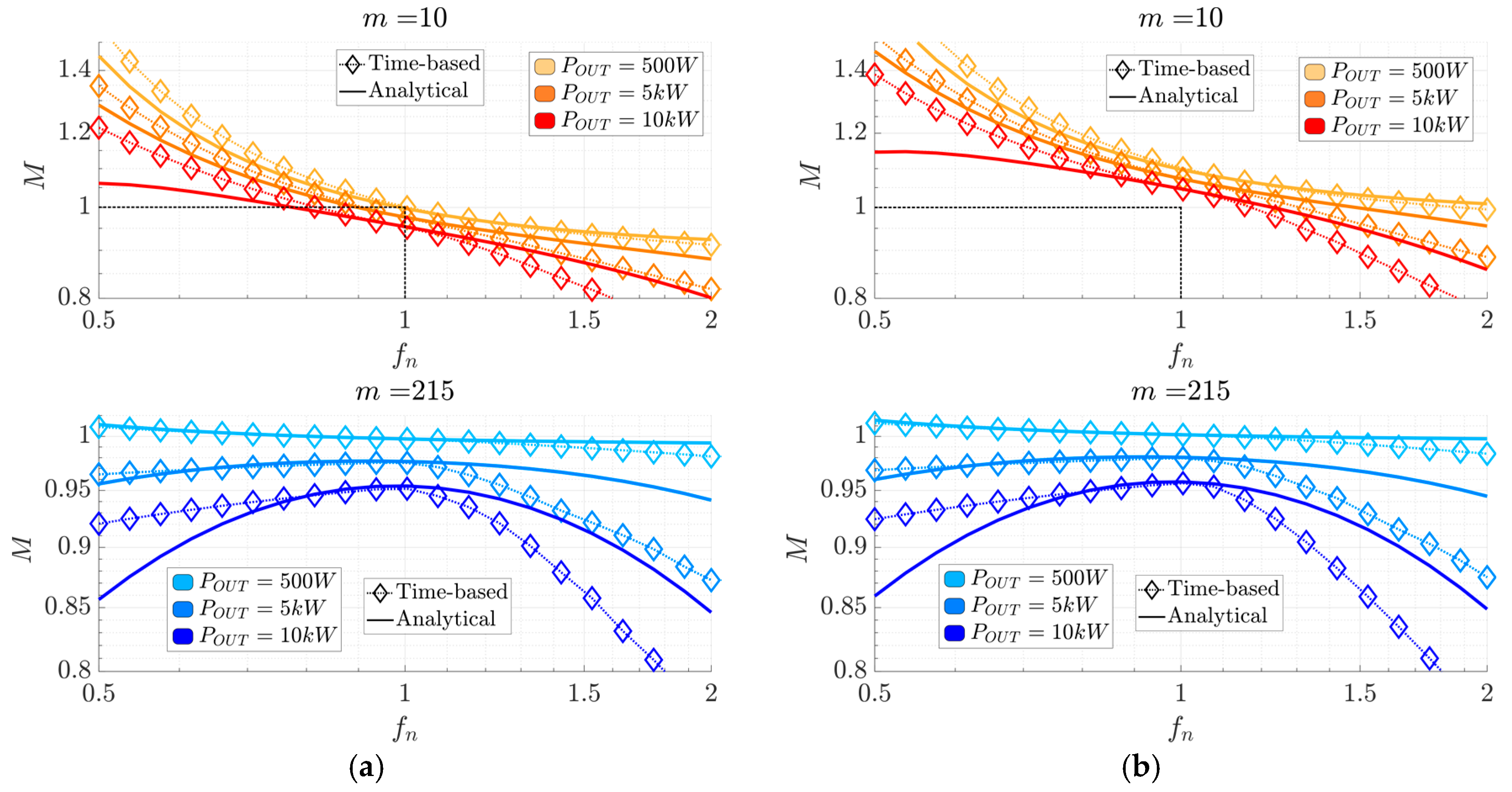
A comparison between the modified FHA and the TB models is depicted in Figure 8. The effect of the voltage drop is visible, as the gain at different power loads does not converge to one point at the resonant frequency. There is a good match between the modified FHA and TB models within the range of 0.75 < f n < 1 . Outside this range, the harmonic content of the resonant current is high enough so that the FHA approach is not valid, especially at high power. Therefore, outside this range, the TB models should be used over the modified FHA for higher accuracy.

2.3. FHA and TB Models Considering Distributed Impedance Model

The use of magnetic integration is widespread in LLC converters in the literature [24,25,26]. With magnetic integration, the two inductors of the LLC converter can be integrated in the transformer as a single magnetic component, where the magnetizing inductance operates as the parallel inductor L m and the leakage inductance as the series resonant inductor L r . However, the equivalent circuit of the transformer is more accurate with distributed leakage inductance if the inductance ratio ( m ) is low, as depicted in Figure 9. Considering external connections, stray inductances and resistances from the PCB and other parasitics, the equivalent model of the distributed LLC can be summarized as the circuit depicted in Figure 10 and Figure 11.
The values of the distributed inductors and resistances are as follows:
( a )   R 1 = ρ R s     ( b )   R 2 = ( 1 ρ ) R s       ( c )   L 1 = λ L r       ( d )   L 2 = ( 1 λ ) L r
where ρ and λ are expressed as numbers between 0 and 1 that establish the distribution between the primary and total series resistance and inductance. The analytical expression for the gain M can be calculated as follows:
M = 1 ( 1 + 1 ( m 1 ) ( 1 ( 1 + A 1 ) f n 2 ) Q Q s + A 2 ) 2 + Q 2 ( ( 1 + B 1 ) f n ( 1 + B 2 ) f n 1 f n 2 · ( 1 ( m 1 ) Q Q s ) ) 2
where the coefficients A 1 , A 2 , B 1 and B 2 are as follows:
( a )   A 1 = ( 1 ρ )   Q Q s               ( b )   A 2 = 1 m 1 [ ρ ( 1 λ ) + ( 1 ρ ) λ ] Q Q s ( 1 λ )     ( c )   B 1 = 1 λ m 1                           ( d )   B 2 = 1 m 1 [ ( 1 λ ) + ρ ( 1 ρ ) Q s 2 ( 1 ρ ) Q Q s ]
It can be observed that when ρ = 1 and λ = 1 , the equivalent circuit becomes that shown in Figure 7, the coefficients A 1 , A 2 , B 1 and B 2 are equal to 0, and Equation (9) yields the same results as Equation (6). All of the coefficients in (10) depend on 1 / ( m 1 ) , except for A 1 , because it is already factorized in Equation (9). For this reason, the distributed model only affects the value of the gain for low values of m . This can be observed in Figure 12a,b, where the gain for m = 215 is the same for both models, while for m = 10 , the gain increases by 10% at resonant frequency.
In conclusion, for high values of m , the distributed model is not necessary and the series resistance model can be used as it gives a similar result. However, for low values of m , the distributed impedance model should be used because it is more accurate.

2.4. Time-Based Models for Current Analysis

The FHA models are based on the first harmonic; as such, the currents are purely sinusoidal. In the analysis of the ZVS transition, the instantaneous current is required and the FHA models are not accurate enough. Time-based models (TB) are then required for an accurate estimation of the instantaneous currents.
Two different TB models can be used, as explained in the previous two subsections: the series resistance model and the distributed impedance model, presented in Figure 5. (a) Modified FHA LLC equivalent circuit with series resistance; (b) time-based (TB) LLC circuit with series resistance. Figure 5b and Figure 9, respectively. The distributed impedance model is closer to reality and gives more accurate results for low frequencies and low inductance ratios, as depicted in the next section in Figure 11.
In the next section, the ZVS transition will be analyzed in detail. However, it is necessary to know which of the two models is required for accurate modeling of the current during this transition.

3. ZVS Analysis for the Unregulated LLC Converter

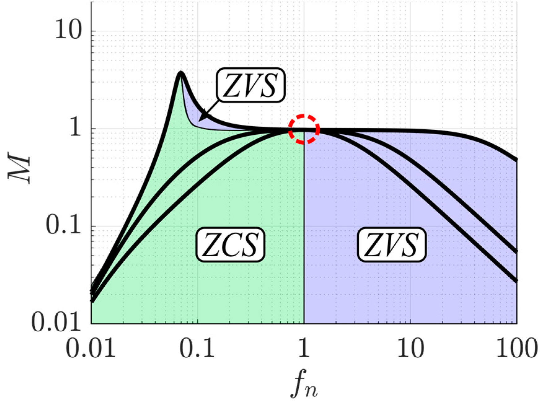
The ZVS and ZCS regions of the LLC converter are depicted in Figure 13. ZVS and ZCS are mutually exclusive, because a turn-off current is needed to achieve a complete ZVS.
The selected topology operates at the resonant frequency where the ZVS regions and the ZCS region meet. In this region, if the turn-off current is small enough, ZCS is not achieved and the ZVS transition will be incomplete (iZVS).
In power converters, ZVS is generally achieved using an inductive current to ensure the charge/discharge transition of the transistor output capacitance ( C o s s ). In the literature [27], this transition is assumed to be at a constant current if the energy stored in the inductor is much higher than the energy in the capacitors:
1 2 L I 2   q o s s _ T o t a l ( V I N ) · V I N
where q o s s _ T o t a l ( V I N ) is the total charge of the output capacitance of a switch. A switch may consist of several transistors in parallel. To avoid confusion with the quality factors, which are traditionally denoted with an uppercase Q , all the charges for the ZVS analysis are denoted with a lowercase q . If the condition in Equation (11) holds, then the turn-off current i o f f ( t ) can be assumed to be constant I o f f and the charge delivered by the inductive current is the following, where t d is the dead-time:
q i = 0 t d i o f f ( t ) · d t
The complete ZVS condition can be derived in terms of available inductive charge ( q i ) compared to the stored charge q o s s _ T o t a l using the following equation:
q i q o s s _ T o t a l .
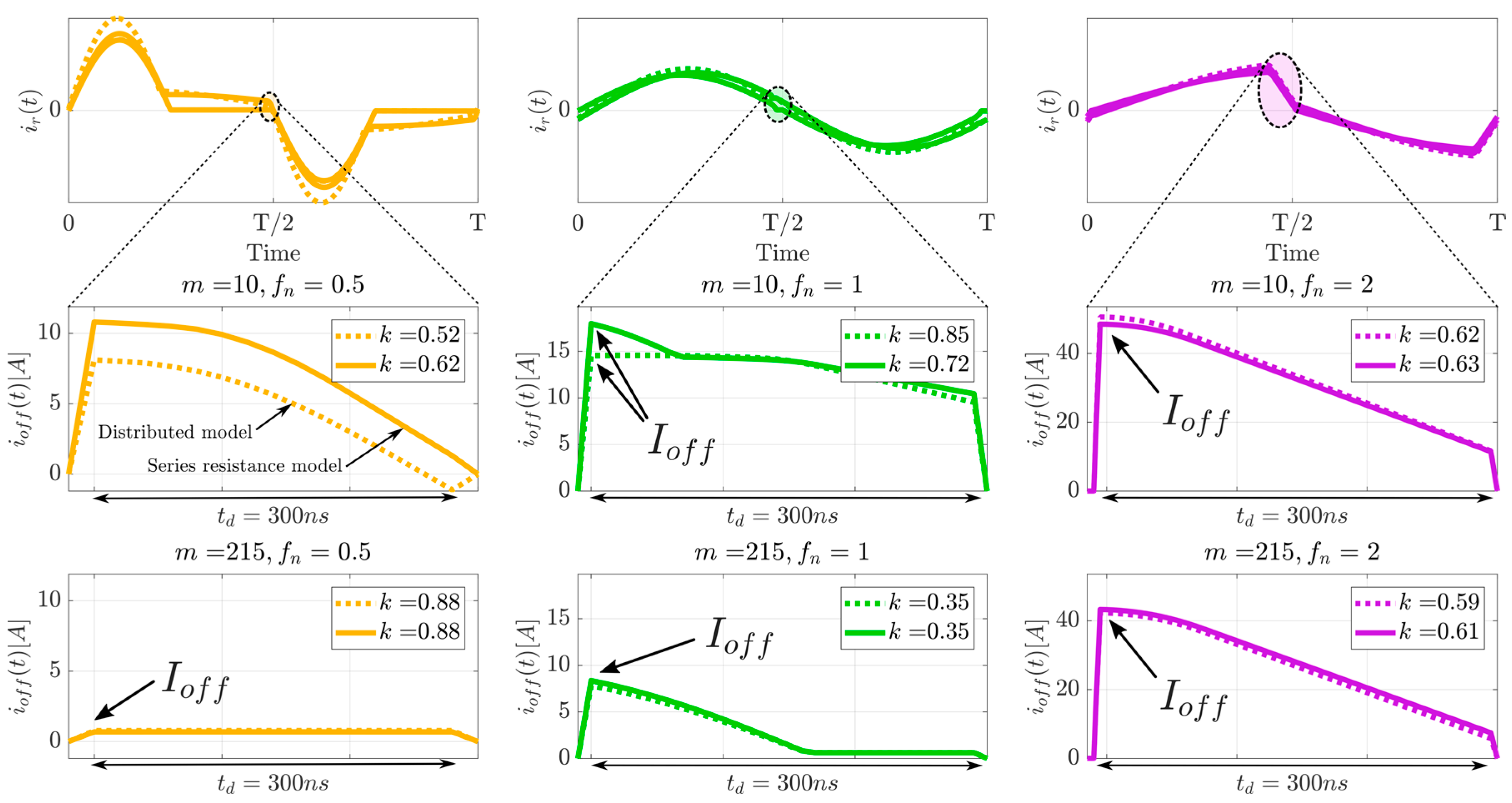
However, in LLC converters, the transition current is not constant, because multiple reactive elements ( L r , L m , C r , ) shape the turn-off current, as illustrated in Figure 14. To account for this, a charge ratio k q can be introduced:
k q = q i I o f f · t d = 0 t d i o f f ( t ) · d t I o f f · t d ,
With this charge ratio, the relation between the initial turn-off current ( I o f f ) and the real charge ( q i ) can be defined for a given dead-time ( t d ). When the turn-off transition occurs at constant current, the charge ratio has a value of k q = 1 . In LLC converters, when the turn-off current has a resonant shape, the value of the charge ratio is k q < 1 , as illustrated in Figure 14.
Complete ZVS transition is achieved when q i is higher than q o s s _ T o t a l (see Equation (13)). For LLC converters, this condition can be estimated using TB models, as depicted in Figure 15. For m = 215 , complete ZVS is achieved above resonance and depends on the output load. However, for m = 10 , the complete ZVS range is greatly improved in the range of 0.6 < f n < 1.5 for the whole load range.
Using the information of Figure 15, it can be concluded that, for LLC converters, complete ZVS can only be achieved for the whole load range at low inductance ratios ( m = 10 ). The best operation point is at resonant frequency, where k q 1 for all loads and the switching losses will be reduced. The low inductance ratio LLC converter can only achieve complete ZVS at heavy loads and operate above resonance when the efficiency is not optimal.

4. Proposed Auxiliary Circuit

An auxiliary circuit is proposed to achieve complete ZVS for the full load range for a high inductance ratio ( m ), where the design of the LLC achieves the highest efficiency and power density. Auxiliary circuits are commonly used in full-bridge converters to improve their ZVS capabilities [16,28], particularly in LLC converters [29].
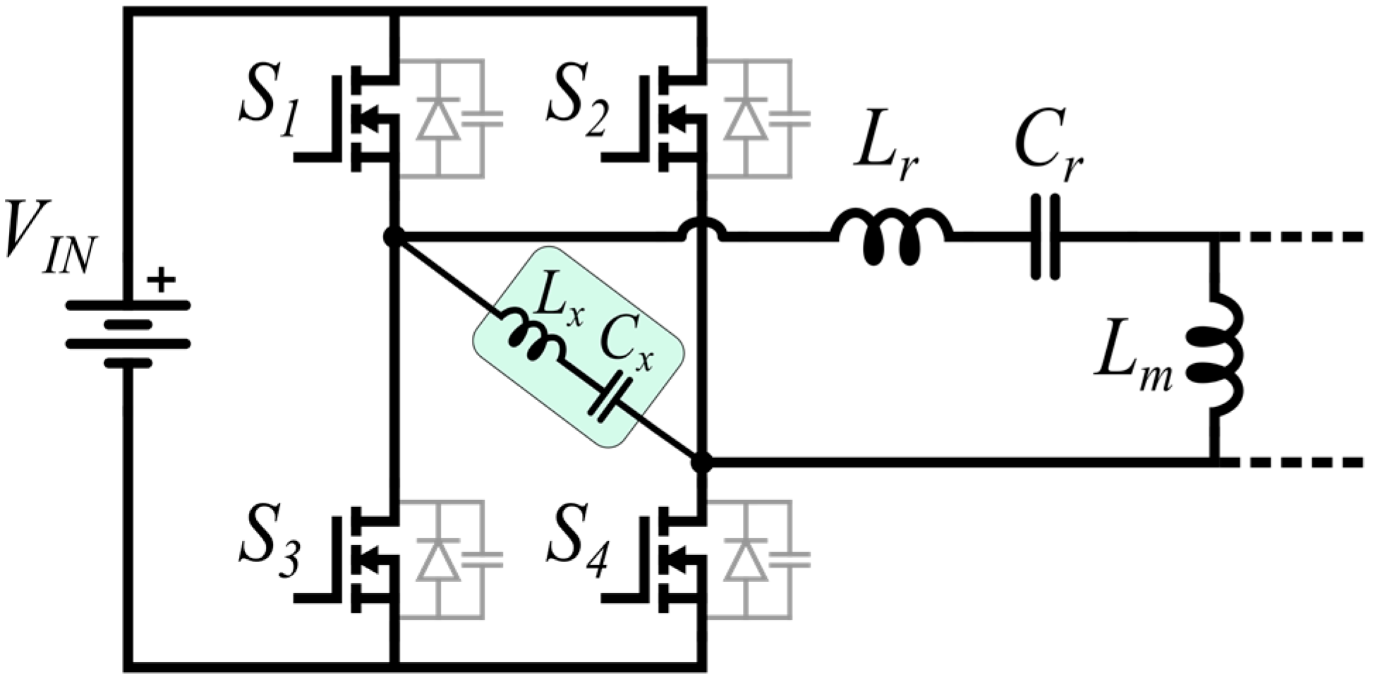
The auxiliary circuit consists of an inductor directly connected to both middle points of the primary full-bridge legs, as depicted in Figure 16. A small-series DC blocking capacitor ( C x ) is added to avoid the core saturation of L x , since the inductor current is not controlled.
The purpose of the auxiliary inductor is to provide a constant current during the ZVS charge/discharge transition, avoiding the issues discussed in the previous section.
The equivalent circuit for FHA analysis is modified as illustrated in Figure 17.
Because the auxiliary circuit is in parallel with the input voltage source, the gain will not be affected by this circuit. Additionally, the resonant frequency of the auxiliary circuit is designed to be much lower than the series resonant tank frequency in order to not affect the series resonant tank frequency. To analyze this circuit, two additional normalized parameters need to be introduced:
  • The normalized auxiliary frequency:
    f x n = f x f r = L r C r L x C x
  • The auxiliary inductance ratio m x :
    m x = L x + L r L r
For simplicity, these parameters are defined similarly to the normalized parameters of the LLC converter.

4.1. Auxiliary Circuit Analysis and Design

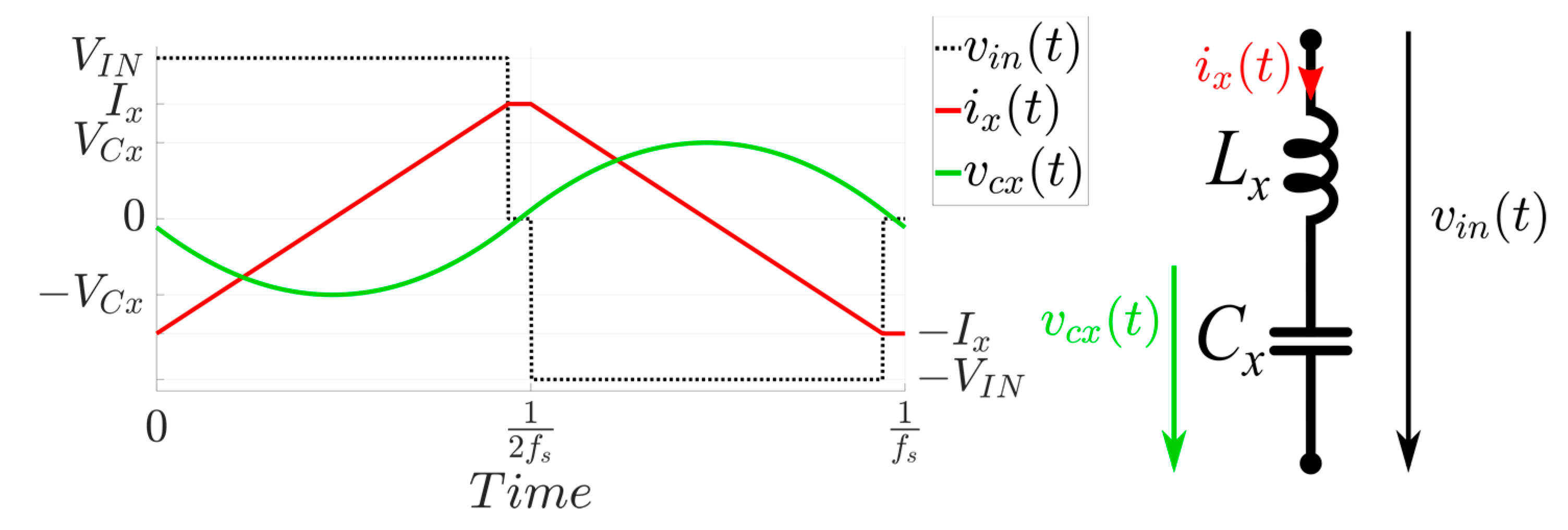
Because the auxiliary circuit is designed to have an inductive behavior at the switching frequency ( f x < f s ), the capacitor voltage ripple can be neglected and the auxiliary inductor voltage is equal to the input bridge square voltage, as depicted in Figure 18.
The triangular inductive peak current can be calculated as follows:
I x = m a x ( i x ( t ) ) = V I N d 2 L x f s = π d n V O U T ( m x 1 ) Z r f n M ,
where d is the duty cycle, and Z r is the equivalent impedance of the series resonant tank.
As explained in the previous section, Equation (13) must hold to achieve complete ZVS. However, with the auxiliary circuit, the total charge is equal to the charge delivered by the LLC tank current and the auxiliary circuit current.
q i = q i x + q i r = k q I o f f t d = k q ( I x + I r ) t d .
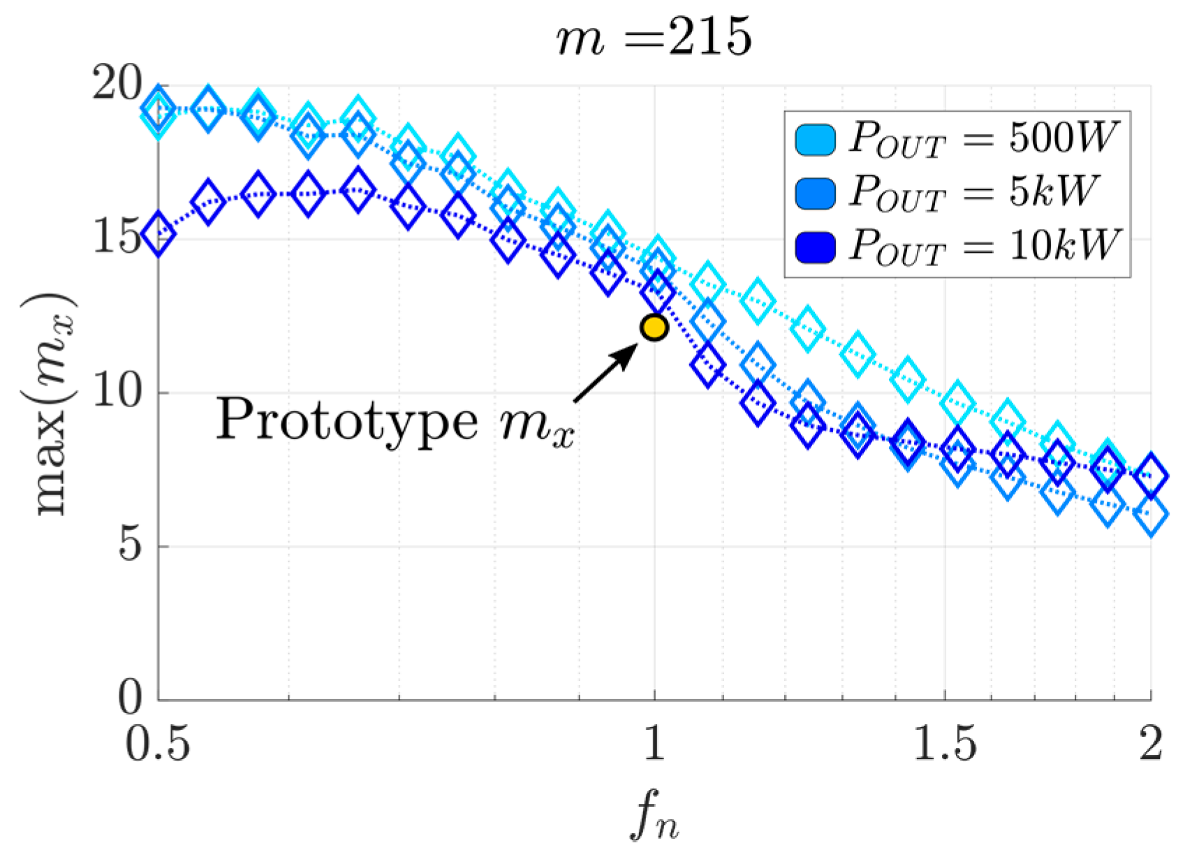
Using Equations (13), (17) and (18), the maximum value for the inductance ratio of the auxiliary circuit m x to ensure complete ZVS for a given t d can be calculated as follows:
m x 1 + π d n V O U T ( q o s s k q · t d I r ) Z r f n M .
As this auxiliary circuit can provide almost all of the charge to achieve complete ZVS, the LLC can be designed with a high magnetizing inductance value to minimize the circulating currents and optimize efficiency, as explained in the first section.
The maximum auxiliary inductance ratio from Equation (19) is plotted at different loads and frequencies in Figure 19. The selected auxiliary inductance ratio for the final prototype is 12.5.
To avoid DC bias in the unregulated inductor, a DC blocking capacitor is added in series. This creates a secondary resonant tank. As explained previously, the auxiliary circuit behavior is inductive. At resonant frequency, where f s = f r , then f x n 1 .
The voltage in the capacitor is negligible compared to the input square waveform. However, the maximum voltage value should be calculated for design purposes. The auxiliary capacitor voltage shape is a parabola, as shown in Figure 18. The ripple in this capacitor can be calculated using the capacitor equation and integrating the triangular current through the auxiliary circuit:
V C x = m a x ( v C x ( t ) ) = v C x ( d 2 f s ) = I x ( 1 3 2 d ) 2 C x f s = ( π ) 2 · d ( 1 3 2 d ) · f x n 2 f n 2 · n V O U T M    
For a value of f x n = 0.1 , the equation yields V C x 0.02 · V I N .

4.2. Transformer Design and Comparison

Using the auxiliary circuit, complete ZVS at a full load range can be achieved without using the magnetizing inductance of the transformer. Therefore, the inductance ratio of the LLC converter can be as high as possible, reducing the circulating currents and improving the efficiency. To show the advantages of a high inductance ratio transformer, two transformers designs are compared.
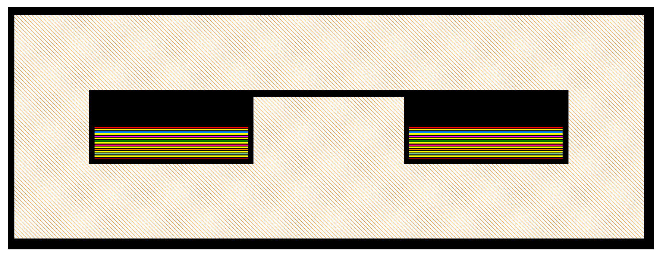
The comparison between the m = 10 transformer design, Figure 20, and the m = 215 transformer with m x = 10 , Figure 21, auxiliary inductor is shown in Table 3. The transformers are divided into two components because a series/parallel configuration is used; this will be explained in the next section.
Transformers with low magnetizing inductance typically use gaps and therefore lead to higher losses and reduced power density [25]. The window utilization of gapped transformers has to be low to avoid the gap proximity effect [30]. The proposed auxiliary circuit increases the magnetic component count but decreases the losses and volume. It can be concluded that the proposed auxiliary circuit is an overall improvement to the power density of the converter and does not add any significant complexity to the control scheme, as it is a passive solution.

5. Prototype

A prototype was built to validate the proposed solution for a 10 kW aircraft application with the parameters shown in Table 4 and Table 5.
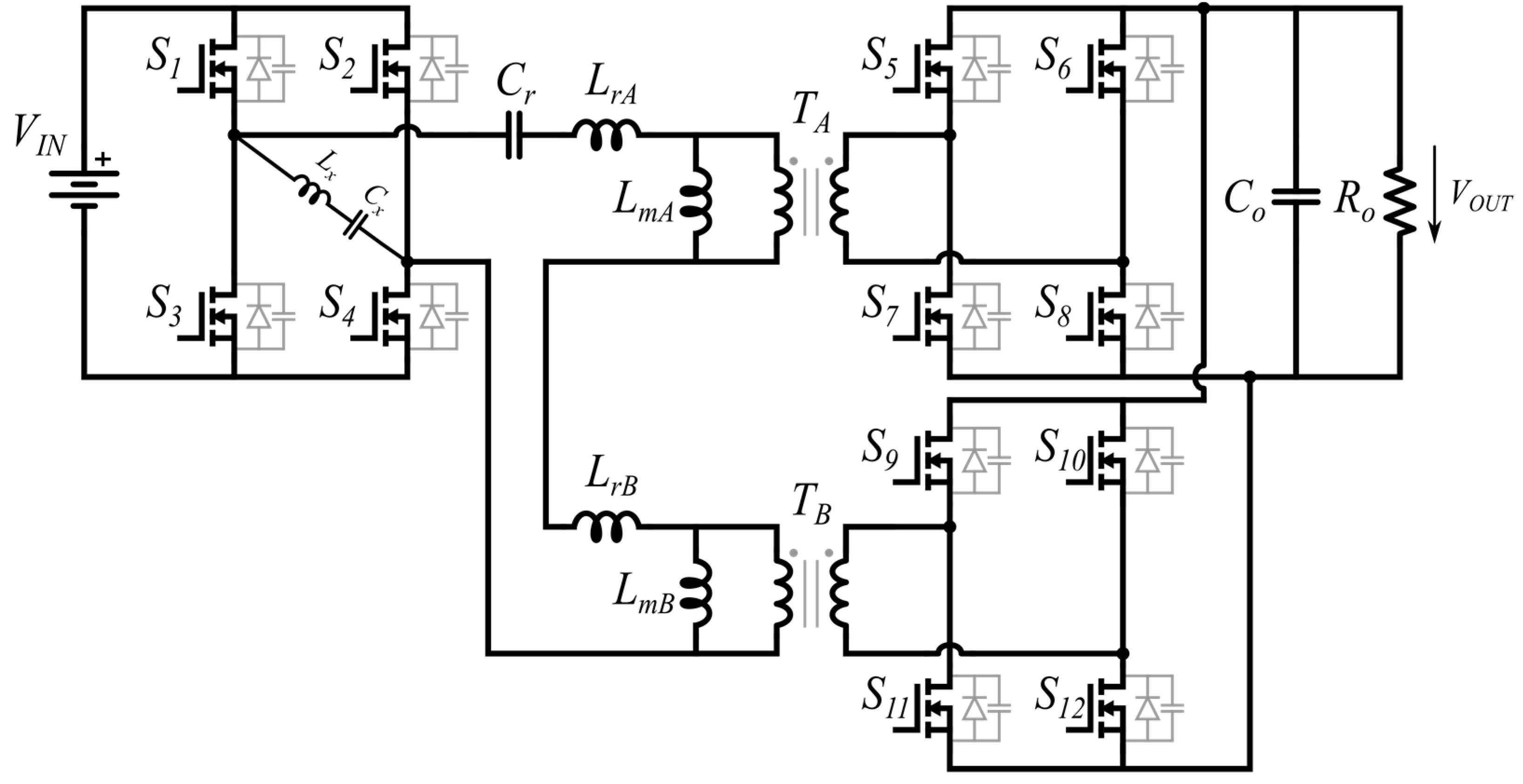
A modified LLC converter topology was used with two series parallel transformers and two output bridges [31], as depicted in Figure 22. This modified structure does not affect the analysis described in previous sections. However, the series inductor L r of the LLC topology consists on the leakage inductances of both transformers in series ( L r A and L r B ), while the parallel inductor L m consists on the two transformers magnetizing inductances in series ( L m A and L m B ). Because the magnetizing inductances of the two transformers are in series in the primary mode, the inductance ratio ( m ) is further increased.
This modified structure is adequate for high-power applications since the two independent output bridges can handle half the load and double the switching devices effectively in parallel. Synchronous output bridges are used to further improve the efficiency. Current sharing in the secondary mode is achieved because of the series connection of the two transformers. Therefore, current measurement or a secondary resonant capacitor are not required. Because the difference in the impedance of each secondary bridge is small, the mismatch in the current sharing will also be small. However, secondary bridge synchronization is important to ensure a balance of DC bias in both transformers; synchronization can occur naturally with higher dead-times and under diode turn-off [5].
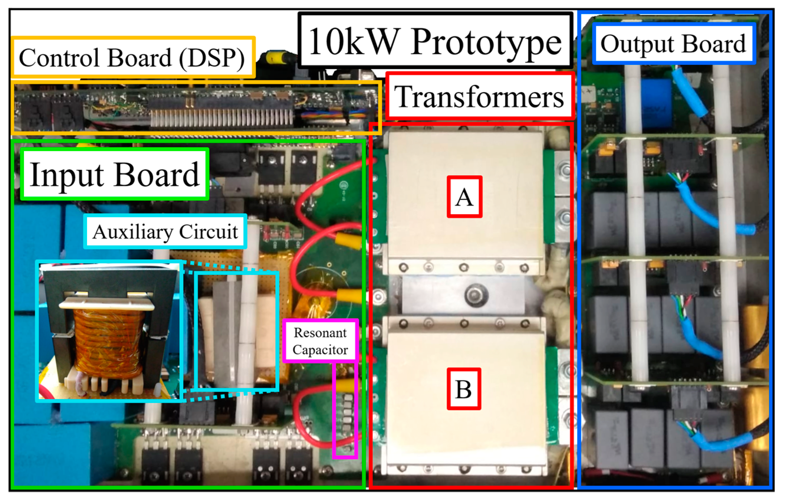
The prototype is depicted in Figure 23 and consists of the input board, the transformers, and the output board, as well as the control board, which provides all transistor signals as well as providing hardware protection.
The components used in the prototype are shown in Table 6. Silicon MOSFET technology is used because it is a robust technology. Because the converter operates with soft-switching, the use of an Si devices does not detract from the efficiency. However, improvements in other types of devices, such as high-voltage GaN technology, could be a candidate for future improvements on the prototype. These devices will further reduce the volume of the auxiliary circuit as they have less output capacitance charge and ZVS is achieved more easily.

6. Experimental Results

Experimental waveforms at the nominal and overload power (5 kW and 10 kW) are depicted in Figure 24. The secondary currents are measured with the inverted polarity of one measurement as they fully overlap and would not otherwise be distinguishable. It can be seen that the current sharing is validated, with a DC mismatch of less than 5% at 10 kW.
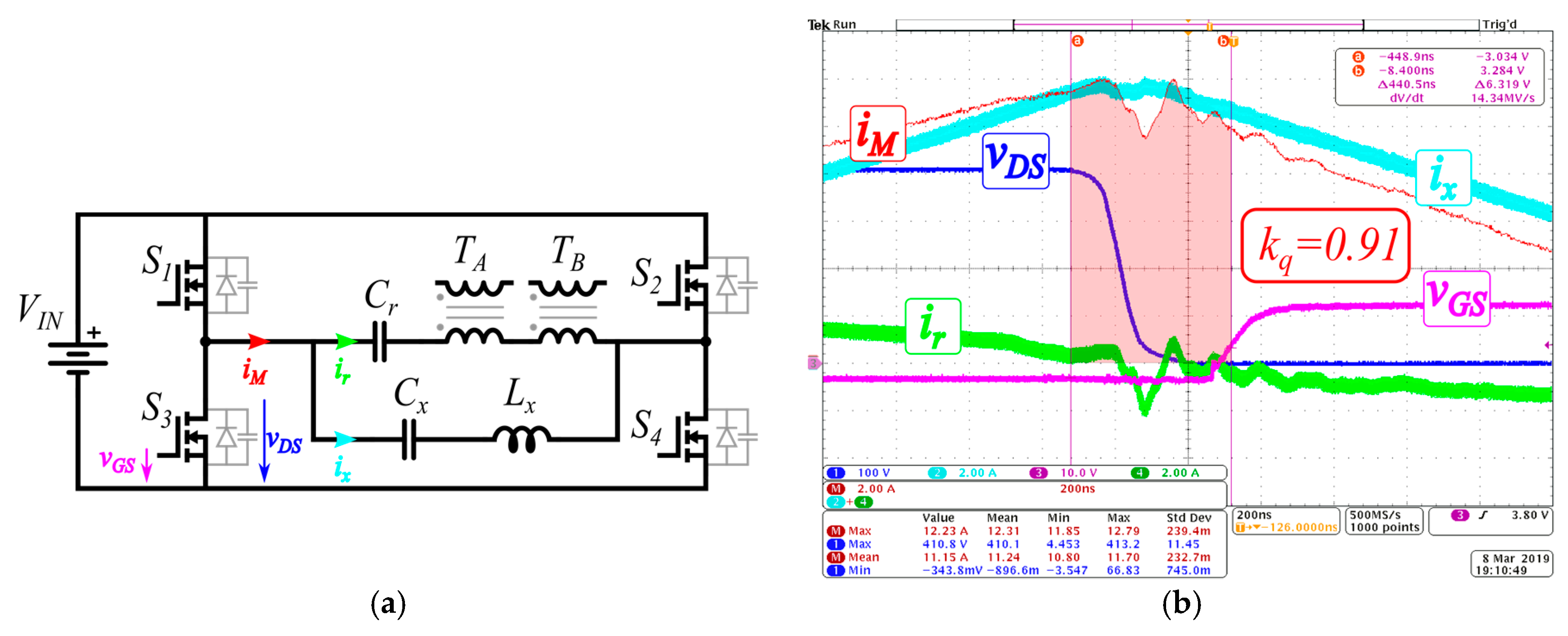
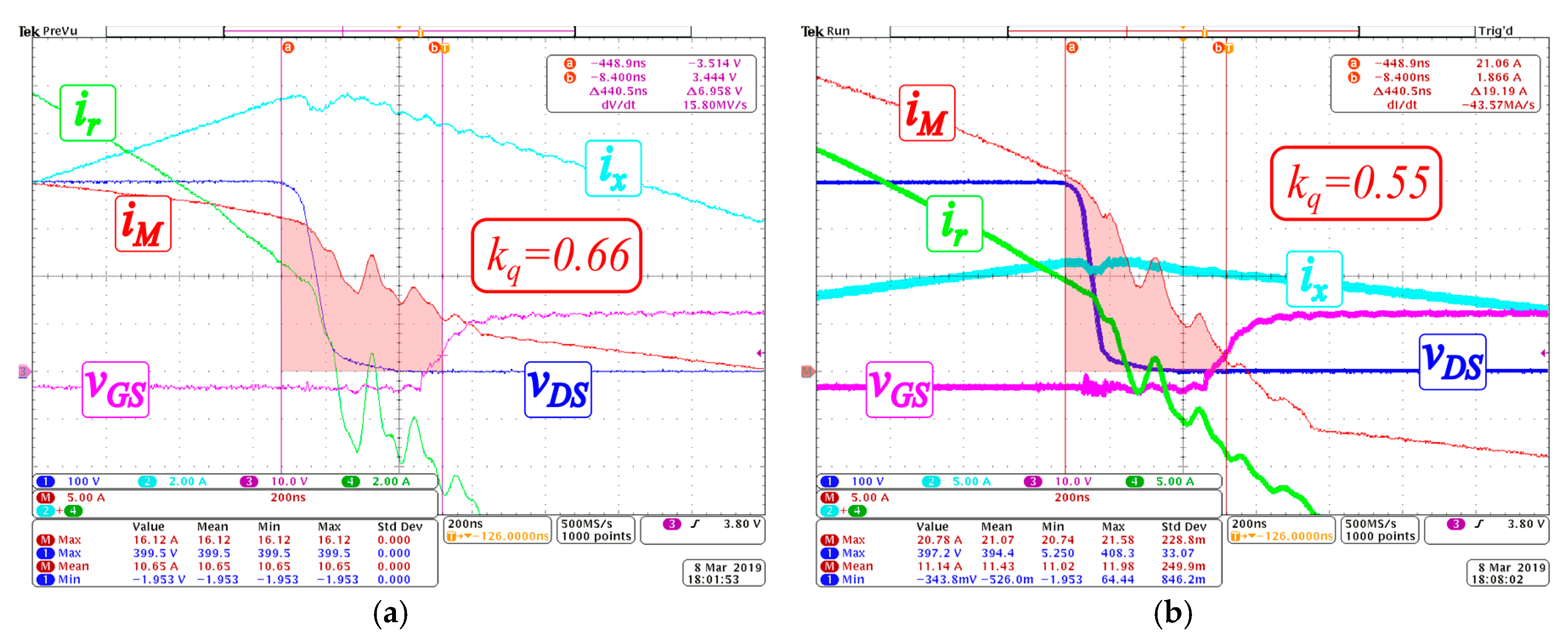
The measurements are depicted in Figure 25a. The experimental results of the ZVS transition are shown in Figure 25b at 500 W (light load), in Figure 26a at 5 kW (nominal load) and in Figure 26b at 10 kW (overload condition). The ZVS transition is achieved completely for all loads as the drain-source voltage of S3 is zero when it is turned on. The charge ratio can be estimated integrating the current between the cursors k q = 0.91 / 0.66 / 0.55 for 500 W, 5 kW and 10 kW, respectively.
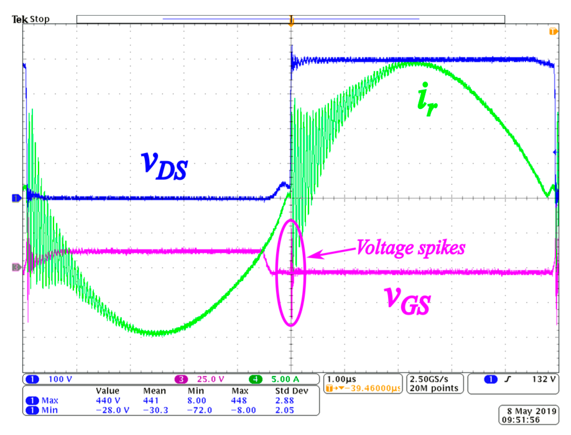
To validate the improvement in efficiency provided by the auxiliary circuit, prototype tests are carried out without the auxiliary circuit. In Figure 27, the resonant current, drain-source and gate-source voltages are shown. ZVS is not achieved and voltages spikes appear in both voltages. The resonant current is distorted by a parasitic resonance between the output capacitor of the MOSFET and the series resonant inductor.
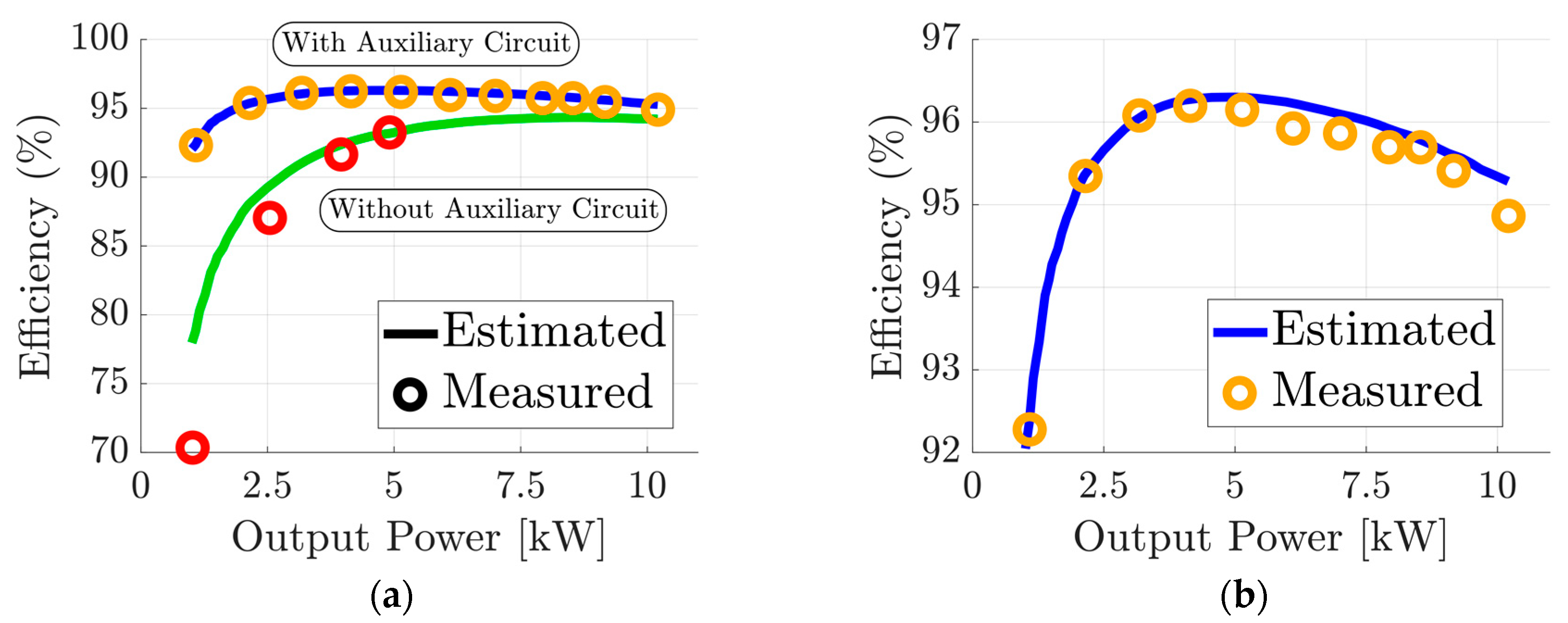
The performance comparison between these two prototype set-ups is depicted in Figure 28a. The efficiency is improved by the inclusion of the auxiliary circuit. Without the auxiliary circuit, ZVS is not achieved and the switching losses are increased.
A close-up of the measured efficiency at different loads is depicted in Figure 28a. The measured efficiency at nominal output power (5 kW) is 96.26% and at the overload power (10 kW) is 94.86%. The estimated efficiency is calculated using the power loss model explained in Section 2. The results show a good match with the estimated values.
The measured load-dependent voltage drop of the gain ( M ) is shown in Figure 28b and follows the modified analytical equation (Equation (6)).

7. Conclusions

This article makes two main contributions: the first is related to the accurate modeling of LLC converters. A series resistance FHA model and a distributed FHA model are proposed and compared with time-based models and are an improvement over the traditional FHA approach. The first model is accurate for high inductance ratio LLC converters, while the second model is more accurate for low inductance ratios. The distributed FHA model has not been experimentally validated, and this can be done as future work. A time-based ZVS analysis is performed using a method based on charge and using time-based models. This analysis considers the variable current along the transition in LLC converters. With this method, the ZVS range is analyzed for different LLC designs. As a conclusion, the most suitable design to achieve ZVS in the whole load range is the low inductance ratio LLC converter, although it is less efficient than the high inductance ratio converter.
As for the second contribution, an auxiliary circuit is proposed to achieve complete ZVS at the whole load range in a high inductance ratio LLC converter. The circuit is analyzed using the charge method proposed. This circuit is designed for an unregulated LLC converter operating at resonant frequency. This solution has higher power density compared with the low inductance ratio LLC converter as it avoids gapped transformer designs.
A 10 kW prototype is designed to validate the auxiliary circuit. The measured efficiency is 96.2% at the 5 kW nominal power and 94.86% at the 10 kW overload power. Experimental results show that complete ZVS is achieved with the auxiliary circuit, at a light load (500 W), nominal load (5 kW) and peak load (10 kW). With the addition of the auxiliary circuit, the efficiency is improved from 93% to 96.2% at 5 kW.

Author Contributions

Conceptualization, Y.E.B. and D.S.; data curation, Y.E.B.; formal analysis, Y.E.B. and D.S.; funding acquisition, J.A.C. and J.C.; investigation, Y.E.B. and P.A.; methodology, Y.E.B., J.A.O. and P.A.; project administration, M.V., J.A.O., P.A. and J.C.; resources, G.M. and J.C.; software, Y.E.B.; supervision, M.V., J.A.O. and P.A.; validation, Y.E.B., U.B. and G.M.; visualization, Y.E.B.; writing—original draft, Y.E.B.; writing—review & editing, Y.E.B., D.S. and P.A.

Funding

This research has been partially supported by the research project DPI2017-88505-C2-1-R (Soluciones optimas para el procesado de la energia de las nuevas plantas solares de 1500V con conexion a la red electrica) funded by the Spanish government (Ministerio de Ciencia, Innovacion y Universidades).

Acknowledgments

The authors thank Isabel Senent and Cheng Li for the help in the review process, and the AIR-Project (E13-0505C-366) for contributing to build the prototype.

Conflicts of Interest

The authors declare no conflict of interest. The funders had no role in the design of the study; in the collection, analyses, or interpretation of data; in the writing of the manuscript, or in the decision to publish the results.

References

  1. Emadi, K.; Ehsani, M. Aircraft power systems: Technology, state of the art, and future trends. IEEE Aerosp. Electron. Syst. Mag. 2000, 15, 28–32. [Google Scholar] [CrossRef]
  2. Rosero, J.A.; Ortega, J.A.; Aldabas, E.; Romeral, L. Moving towards a more electric aircraft. IEEE Aerosp. Electron. Syst. Mag. 2007, 22, 3–9. [Google Scholar] [CrossRef] [Green Version]
  3. Jones, R.I. The more electric aircraft: The past and the future? In Proceedings of the IEE Colloquium Electrical Machines and Systems for the More Electric Aircraft, London, UK, 9 November 1999; p. 1. [Google Scholar]
  4. Zhao, X.; Guerrero, J.M.; Wu, X. Review of aircraft electric power systems and architectures. In Proceedings of the 2014 IEEE International Energy Conference (ENERGYCON), Cavtat, Croatia, 13–16 May 2014; pp. 949–953. [Google Scholar]
  5. Bouvier, Y.E.; Borović, U.; Vasić, M.; Oliver, J.A.; Alou, P.; Cobos, J.A.; Árevalo, F.; García-Tembleque, J.C.; Carmena, J. DC/DC fixed frequency resonant LLC full-bridge converter with series-parallel transformers for 10 kW high efficiency aircraft application. In Proceedings of the 2017 IEEE Energy Conversion Congress and Exposition (ECCE), Cincinnati, OH, USA, 1–5 October 2017; pp. 3788–3795. [Google Scholar]
  6. Borovic, U.; Zhao, S.; Silva, M.; Bouvier, Y.E.; Vasić, M.; Oliver, J.A.; Alou, P.; Cobos, J.A.; Árevalo, F.; García-Tembleque, J.C.; et al. Comparison of three-phase active rectifier solutions for avionic applications: Impact of the avionic standard DO-160 F and failure modes. In Proceedings of the 2016 IEEE Energy Conversion Congress and Exposition (ECCE), Milwaukee, WI, USA, 18–22 September 2016; pp. 1–8. [Google Scholar]
  7. Bell, B.; Hari, A. Topology key to Power Density in Isolated DC-DC Converters. Available online: https://pdfs.semanticscholar.org/fbac/b2391b4df41435779e2c69690ef052db2481.pdf (accessed on 14 May 2019).
  8. Yeon, C.-O.; Park, M.-H.; Ko, S.-H.; Lim, C.-Y.; Jang, Y.-J.; Moon, G.-W.; Kang, F.-S. A new LLC resonant converter with resonant frequency change for high conversion efficiency and high power density. In Proceedings of the 2017 IEEE 3rd International Future Energy Electronics Conference and ECCE Asia (IFEEC 2017-ECCE Asia), Kaohsiung, Taiwan, 3–7 June 2017; pp. 265–269. [Google Scholar]
  9. Fei, C.; Lee, F.C.; Li, Q. High-efficiency high-power-density LLC converter with an integrated planar matrix transformer for high-output current applications. IEEE Trans. Ind. Electron. 2017, 64, 9072–9082. [Google Scholar] [CrossRef]
  10. Pavlovic, Z.; Oliver, J.A.; Alou, P.; Garcia, Ó.; Cobos, J.A. Bidirectional multiple port dc/dc transformer based on a series resonant converter. In Proceedings of the 2013 Twenty-Eighth Annual IEEE Applied Power Electronics Conference and Exposition (APEC), Long Beach, CA, USA, 17–21 March 2013. [Google Scholar]
  11. Tomas-Manez, K.; Zhang, Z.; Ouyang, Z. Unregulated series resonant converter for interlinking DC nanogrids. In Proceedings of the 2017 IEEE 12th International Conference on Power Electronics and Drive Systems (PEDS), Honolulu, HI, USA, 12–25 December 2017; pp. 647–654. [Google Scholar]
  12. Gopiyani, A.; Patel, V.; Shah, M.T. A novel half-bridge LLC resonant converter for high power DC power supply. In Proceedings of the 2010 Conference Proceedings IPEC, Singapore, 27–29 October 2010; pp. 34–39. [Google Scholar]
  13. Hu, S.; Deng, J.; Mi, C.; Zhang, M. LLC resonant converters for PHEV battery chargers. In Proceedings of the 2013 Twenty-Eighth Annual IEEE Applied Power Electronics Conference and Exposition (APEC), Long Beach, CA, USA, 17–21 March 2013; pp. 3051–3054. [Google Scholar]
  14. Fu, D.; Lu, B.; Lee, F.C. 1MHz high efficiency LLC resonant converters with synchronous rectifier. In Proceedings of the 2007 IEEE Power Electronics Specialists Conference, Orlando, FL, USA, 17–21 June 2007; pp. 2404–2410. [Google Scholar]
  15. Zhang, X.; Chen, W.; Ruan, X.; Yao, K. A novel ZVS PWM phase-shifted full-bridge converter with controlled auxiliary circuit. In Proceedings of the 2009 Twenty-Fourth Annual IEEE Applied Power Electronics Conference and Exposition, Washington, DC, USA, 15–19 February 2009; pp. 1067–1072. [Google Scholar]
  16. Safaee, A.; Jain, P.; Bakhshai, A. A robust low-RMS-current passive auxiliary circuit for ZVS operation of both legs in full bridge converters. In Proceedings of the 2015 IEEE Applied Power Electronics Conference and Exposition (APEC), Charlotte, NC, USA, 15–29 March 2015; pp. 21–27. [Google Scholar]
  17. Chen, W.; Ruan, X.; Ge, J. A novel full-bridge converter achieving ZVS over wide load range with a passive auxiliary circuit. In Proceedings of the 2010 IEEE Energy Conversion Congress and Exposition, Atlanta, GA, USA, 12–16 September 2010; pp. 1110–1115. [Google Scholar]
  18. Safaee, A.; Jain, P.K.; Bakhshai, A. An adaptive ZVS full-bridge DC–DC converter with reduced conduction losses and frequency variation range. IEEE Trans. Power Electron. 2015, 30, 4107–4118. [Google Scholar] [CrossRef]
  19. Steigerwald, R.L. A comparison of half-bridge resonant converter topologies. IEEE Trans. Power Electron. 1988, 3, 174–182. [Google Scholar] [CrossRef]
  20. Huang, H. FHA-based voltage gain function with harmonic compensation for LLC resonant converter. In Proceedings of the 2010 Twenty-Fifth Annual IEEE Applied Power Electronics Conference and Exposition (APEC), Palm Springs, CA, USA, 21–25 February 2010; pp. 1770–1777. [Google Scholar]
  21. Liu, J.; Zhang, J.; Zheng, T.Q.; Yang, J. A modified gain model and the corresponding design method for an LLC resonant converter. IEEE Trans. Power Electron. 2017, 32, 6716–6727. [Google Scholar] [CrossRef]
  22. Graovac, D.; Purschel, M.; Andreas, K. MOSFET Power Losses Calculation Using the Data-Sheet Parameters; Infineon Technologies AG: Neubiberg, Germany, 2006. [Google Scholar]
  23. Li, J.; Abdallah, T.; Sullivan, C.R. Improved calculation of core loss with nonsinusoidal waveforms. In Proceedings of the Conference Record of the 2001 IEEE Industry Applications Conference. 36th IAS Annual Meeting (Cat. No.01CH37248), Chicago, IL, USA, 30 September–4 October 2001; Volume 4, pp. 2203–2210. [Google Scholar]
  24. de Simone, S.; Adragna, C.; Spini, C. Design guideline for magnetic integration in LLC resonant converters. In Proceedings of the 2008 International Symposium on Power Electronics, Electrical Drives, Automation and Motion, Ischia, Italy, 11–13 June 2008; pp. 950–957. [Google Scholar]
  25. Zhang, J.; Hurley, W.G.; Wolfle, W.H. Gapped transformer design methodology and implementation for LLC resonant converters. IEEE Trans. Ind. Appl. 2016, 52, 342–350. [Google Scholar] [CrossRef]
  26. Yang, B.; Chen, R.; Lee, F.C. Integrated magnetic for LLC resonant converter. In Proceedings of the APEC. Seventeenth Annual IEEE Applied Power Electronics Conference and Exposition (Cat. No.02CH37335), Dallas, TX, USA, 10–14 March 2002; pp. 346–351. [Google Scholar]
  27. Kasper, M.; Burkat, M.R.; Deboy, G.; Kolar, J.W. ZVS of power MOSFETs revisited. IEEE Trans. Power Electron. 2016, 31, 8063–8067. [Google Scholar] [CrossRef]
  28. Borage, M.; Tiwari, S.; Kotaiah, S. A passive auxiliary circuit achieves zero-voltage-switching in full-bridge converter over entire conversion range. IEEE Power Electron. Lett. 2005, 3, 141–143. [Google Scholar] [CrossRef]
  29. Kim, D.-K.; Moon, S.; Yeon, C.-O.; Moon, G.-W. High efficiency LLC resonant converter with high voltage gain using auxiliary LC resonant circuit. IEEE Trans. Power Electron. 2016, 31, 6901–6909. [Google Scholar] [CrossRef]
  30. Prieto, R.; Cobos, J.A.; Garcia, O.; Alou, P.; Uceda, J. High frequency resistance in flyback type transformers. In Proceedings of the APEC 2000. Fifteenth Annual IEEE Applied Power Electronics Conference and Exposition (Cat. No.00CH37058), New Orleans, LA, USA, 6–10 February 2000; Volume 2, pp. 714–719. [Google Scholar]
  31. Lin, B.R.; Chen, P.L.; Huang, C.L. Analysis of LLC converter with series-parallel connection. In Proceedings of the 2010 5th IEEE Conference on Industrial Electronics and Applications, Taichung, Taiwan, 15–17 June 2010; pp. 346–351. [Google Scholar]
Figure 1. Aircraft active isolated rectifier architecture.
Energies 12 01850 g001
Figure 2. Isolated LLC full-bridge with full-bridge diode rectifier.
Energies 12 01850 g002
Figure 3. (a) LLC equivalent circuit (simplified first harmonic approximation (FHA)), (b) LLC voltage gain ( M ) at different inductance ratios ( m ) and quality factors ( Q ).
Energies 12 01850 g003
Figure 4. LLC converter modes: (a) below resonance; (b) at resonant; (c) above resonance.
Energies 12 01850 g004
Figure 5. LLC converter total normalized power losses ( P L o s s / P O U T ) at 10 kW output power. Including primary and secondary transistors and transformer. (a) for m = 10 ; (b) for m = 215 .
Energies 12 01850 g005
Figure 6. LLC converter total normalized power losses ( P L o s s / P O U T ) at 500 W output power, including primary and secondary transistors and a transformer; (a) for m = 10 ; (b) for m = 215 .
Energies 12 01850 g006
Figure 7. (a) Modified FHA LLC equivalent circuit with series resistance; (b) time-based (TB) LLC circuit with series resistance.
Energies 12 01850 g007
Figure 8. Comparison of the gain ( M ) for the modified FHA and TB models (with simulation) with series resistance at different output powers (a) for m = 10 ; (b) for m = 215 .
Energies 12 01850 g008
Figure 9. Equivalent circuit for transformer and external parasitics.
Energies 12 01850 g009
Figure 10. Modified FHA LLC equivalent circuit with distributed inductances and resistances.
Energies 12 01850 g010
Figure 11. TB LLC circuit with distributed inductances and resistances.
Energies 12 01850 g011
Figure 12. Comparison of the gain ( M ) for the series resistance model (Figure 5a) and distributed model (Figure 5b) with the FHA model and time-based simulations: (a) series resistance model gain at different powers and inductance ratios (Figure 6); (b) distributed model gain at different powers and inductance ratios.
Energies 12 01850 g012
Figure 13. Zero voltage switching (ZVS) regions of the LLC converter.
Energies 12 01850 g013
Figure 14. Time-based (TB) simulated currents of each mode and close-up of the dead-time transition for different LLC converter operation modes.
Energies 12 01850 g014
Figure 15. Time-based model simulations: inductive charge ( q i ) and transistor output capacitor charge ( q o s s _ T o t a l ), where iZVS stands for incomplete ZVS. (a) for m = 10 ; (b) for m = 215 .
Energies 12 01850 g015
Figure 16. Proposed auxiliary circuit.
Energies 12 01850 g016
Figure 17. FHA equivalent circuit with auxiliary circuit.
Energies 12 01850 g017
Figure 18. Auxiliary circuit current and voltage and auxiliary capacitor voltage ripple.
Energies 12 01850 g018
Figure 19. Auxiliary circuit maximum inductance ratio ( m x ) design criteria.
Energies 12 01850 g019
Figure 20. Design II: gapped transformer for m = 10 , with a custom core and the same winding configuration and scale.
Energies 12 01850 g020
Figure 21. Design I: forward-type transformer for m = 215 : planar E-core and 200 μm copper foil.
Energies 12 01850 g021
Figure 22. LLC full-bridge with a series parallel transformer configuration and two output-synchronous full-bridges.
Energies 12 01850 g022
Figure 23. 10 kW prototype.
Energies 12 01850 g023
Figure 24. Experimental results: secondary transformer current (magenta and black), input resonant current (cyan), input voltage bridge (blue); (a) at 5 kW of output power; (b) at 10 kW of output power.
Energies 12 01850 g024
Figure 25. (a) Measurement setup including auxiliary circuit; (b) ZVS experimental results at 500 W.
Energies 12 01850 g025
Figure 26. ZVS experimental results: (a) at 5 kW (b) at 10 kW.
Energies 12 01850 g026
Figure 27. Experimental results without auxiliary circuit at 5 kW.
Energies 12 01850 g027
Figure 28. Experimental results: (a) efficiency at different output powers with (blue and yellow) and without (green and red) the auxiliary circuit, (b) close-up of the efficiency with the auxiliary circuit.
Energies 12 01850 g028
Table 1. Isolated DC/DC converter specification.
Input VoltageOutput VoltageOutput PowerOutput Current
400 V28 V10 kW360 A
Table 2. LLC converter normalized parameters.
Normalized frequencyInductance ratio
f n = f s f r = 2 π f s L r C r m =   L m + L r L r
Load quality factorNormalized voltage gain
Q = 1 R O * L r C r M =   n V O U T V I N
Table 3. Breakdown of losses, volume, and temperature of the two magnetic component designs.
Transformers 1Auxiliary InductorTotal Losses 1Total Volume 1
Power LossΔθVolumePower LossΔθVolume
PCuPFePCuPFe
Design I9.8 W13 W61 °C0.18 dm32.0 W2.2 W55 °C0.13 dm349.8 W0.49 dm3
Design II25.5 W18 W101 °C0.37 dm3----87 W0.74 dm3
1 There are two transformers in the design, as the final prototype uses a series parallel configuration. The total volume and losses include the two transformers.
Table 4. Normalized parameters of the prototype.
Q (500 W)Q (5 kW)Q (10 kW)QSmmxfnfxn
0.020.180.367.521512.50.990.023
Table 5. Parameters of the prototype.
LrCrLmLxCxRsfrfs
7.11 μH349 nF2 × 750 μH74 μH60 μF602 mΩ102 kHz101 kHz
Table 6. Prototype components.
ComponentReferenceTypeQuantity
Input capacitorB32778G8606KFilm5
Primary transistorsIPW65R037C6Coolmos8
Resonant capacitorC4532C0G2E473J320KAMultilayer Ceramic6
C3225C0G2E103J160KA3
Transformer corePlanar E-coreFerrite2
Transformer windingCopper foil200 μm-
Secondary transistorsIPP10004S2L-03Optimos32
Output capacitorsB32774D4226J000Film12
Auxiliary inductor coreE65/32/27Ferrite1