Article

Design Methodology of Tightly Regulated Dual-Output LLC Resonant Converter Using PFM-APWM Hybrid Control Method †

Ulsan National Institute of Science and Technology (UNIST), Ulsan KS017, Korea
*
Author to whom correspondence should be addressed.
This paper is an extended version of our paper published in Park, H.; Kim, M.; Jung, J. Tightly regulated dual-output half-bridge converter using PFM-APWM hybrid control method. In Proceedings of the IEEE Applied Power Electronics Conference and Exposition (APEC), Tampa, FL, USA, 26–30 March 2017; pp. 2022–2026.
Energies 2019, 12(11), 2146; https://doi.org/10.3390/en12112146
Submission received: 15 May 2019 / Revised: 2 June 2019 / Accepted: 3 June 2019 / Published: 4 June 2019
(This article belongs to the Special Issue Advances in High-Efficiency LLC Resonant Converters)

Abstract

:
A dual-output LLC resonant converter using pulse frequency modulation (PFM) and asymmetrical pulse width modulation (APWM) can achieve tight output voltage regulation, high power density, and high cost-effectiveness. However, an improper resonant tank design cannot achieve tight cross regulation of the dual-output channels at the worst-case load conditions. In addition, proper magnetizing inductance is required to achieve zero voltage switching (ZVS) of the power MOSFETs in the LLC resonant converter. In this paper, voltage gain of modulation methods and steady state operations are analyzed to implement the hybrid control method. In addition, the operation of the hybrid control algorithm is analyzed to achieve tight cross regulation performance. From this analysis, the design methodology of the resonant tank and the magnetizing inductance are proposed to compensate the output error of both outputs and to achieve ZVS over the entire load range. The cross regulation performance is verified with simulation and experimental results using a 190 W prototype converter.

1. Introduction

Nowadays, many industry fields require well-regulated multiple output voltages to guarantee the stable operation of products, such as ultra-high-definition (UHD) TVs, computers, and other home appliances. To satisfy this requirement, point-of-use power supplies (PUPS) have been used for multiple output applications. However, this method has disadvantages of bulky size and low cost-effectiveness with many power converter modules [1]. Therefore, tightly regulated multiple output converters have been developed to improve the power density and the cost-effectiveness.
In previous research for multiple output converters, cross regulation methods have been popular, since they require output voltage sensors to obtain the output voltage regulation. However, wide load variations between the multiple output channels induce large output voltage error [2,3,4,5,6,7]. The secondary side post regulators (SSPR) have been proposed to tightly regulate the output voltage with small output voltage error. They can regulate each output voltage independently, however, additional switches, gate driving circuits, and voltage controllers are required [8,9,10,11,12,13,14,15,16,17,18,19,20].
In terms of topology, the LLC resonant converter is attractive for several applications, because it has soft switching capability and a small number of resonant components [21,22,23,24]. In previous research of the multiple output LLC resonant converter, the cross regulation technique has been used to regulate multiple output voltages [25,26]. In addition, the SSPR has been used to achieve tight output voltage regulation for the LLC resonant converter [27,28,29,30]. The LLC resonant converter using conventional control methods has the tradeoff between the cost effectiveness and regulation performance.
To obtain the high cost-effectiveness and tight output voltage regulation, the concept of a hybrid control method employing PFM and APWM was introduced for the dual-output LLC resonant converter in [31]. It does not require any additional components to implement the hybrid control algorithm, which shows the same cost-effectiveness as the conventional cross regulation method. However, it can only be applied to the dual-output converter. This previous research shows the preliminary operational principle and the decoupling algorithm to regulate the output voltages using the hybrid algorithm [32]. However, the previous research only shows the preliminary concept of the hybrid control algorithm. Therefore, the available voltage gain design, resonant tank design, and magnetizing inductance design are necessary to implement the hybrid control algorithm for the entire load condition with high power conversion efficiency.
In this paper, the design methodology of the dual-output LLC resonant converter with a hybrid control algorithm are proposed to regulate the output voltage with zero output voltage error and to obtain the ZVS capability for the entire load condition. The available voltage gain range is analyzed to implement the hybrid control algorithm. The design methodology of proper magnetizing inductance is proposed to achieve ZVS on the primary MOSFETs for the entire load range. The proper resonant tank design is proposed to compensate output voltage error for the worst-case load condition. In Section 4, the regulation performance of the dual-output LLC resonant converter with the hybrid control algorithm is verified through simulation and experimental results using a 190 W prototype converter.

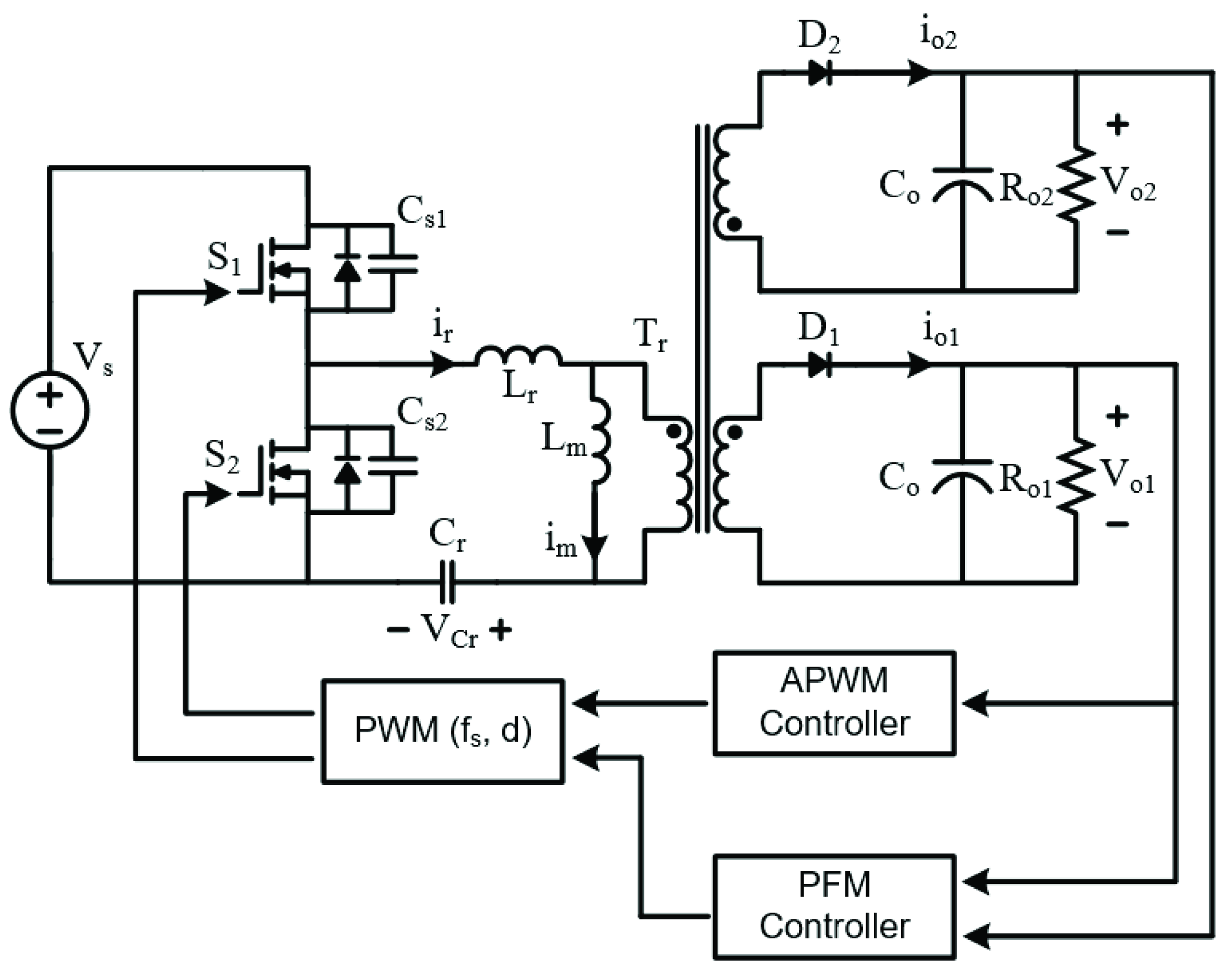
2. Analysis of Dual-Output LLC Resonant Converter

The dual-output LLC resonant converter has the half-bridge structure of a primary inverting stage, a single transformer, and two output channels with diode rectifiers, as shown in Figure 1.

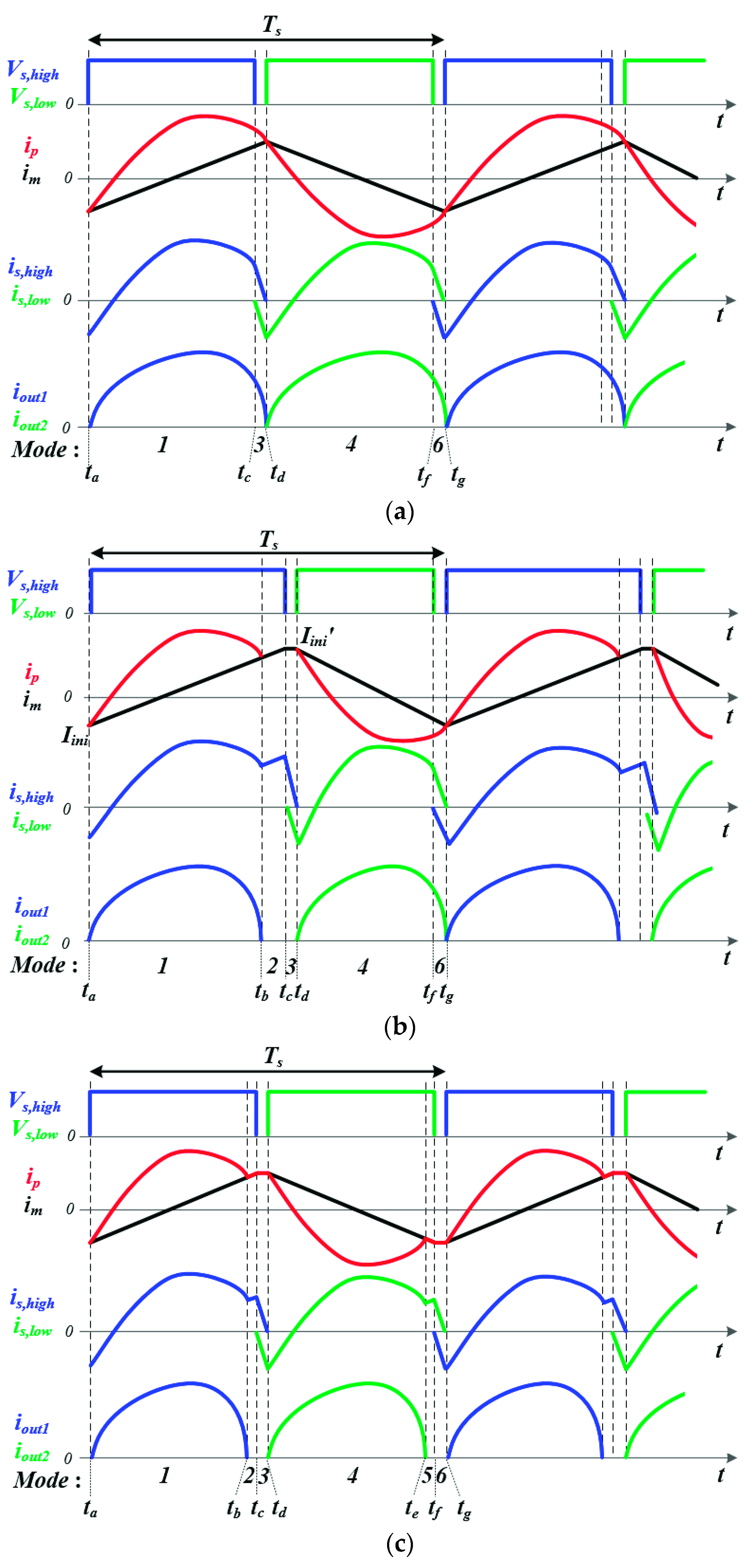
2.1. Operational Principle

Figure 2 shows the operation modes of the dual-output LLC resonant converter, which is divided into six modes during a single switching period. Mode 4 to Mode 6 are repeated from the previous half switching cycle. Figure 3 shows the operational waveforms of the dual-output converter. Mode 1 and 4 are a series resonant mode between the resonant inductance and the resonant capacitance. During Mode 1, the proposed converter transfers electric power in the primary side to Vo1 in the secondary side. The primary and magnetizing current for Mode 1 can be derived as follows:
i r ( t ) = I i n i cos ( ω r t ) + C r ω r ( V i n n V o 1 V c r , i n i ) sin ( ω r t ) i m ( t ) = I i n i + n V o 1 L m t
where Iini is the initial magnetizing current, Cr is the resonant capacitance, Lm is the magnetizing inductance, ωr is the resonant angular frequency, Vin is the input voltage, n is the primary to secondary transformer turn ratio, Vo1 is the one output voltage, and Vcr is the initial resonant capacitor voltage. During Mode 4, the converter transfers electric power to the Vo2 side. The primary and magnetizing current for Mode 4 can be derived as follows:
i r ( t ) = I i n i cos ( ω r t ) + C r ω r ( V c r , i n i n V o 2 ) sin ( ω r t ) i m ( t ) = I i n i n V o 2 L m t
where Iini′ is the initial magnetizing current, and Vcr,ini′ is the initial resonant capacitor voltage.
Mode 2 and 5 are parallel resonant modes among the resonant inductance, the magnetizing inductance, and the resonant capacitance. Those modes guarantee soft commutation on the secondary side diode rectifiers. Mode 3 and 6 are the dead time durations of the primary switch. During Mode 3 and 6, the output capacitance of the power switches is charged and discharged to obtain the ZVS. In steady state, the dual-output converter using the hybrid control algorithm can operate under a four operation mode (Case A), a five operation mode (Case B), and a six operation mode (Case C) according to output power conditions.
The light load condition makes the Case A operation, which induces no soft commutation on all output rectifiers during Mode 3 and 6. From middle to full load condition the converter operates according to Case B, which induces soft commutation on the diode of the Vo1 channel during Mode 2 and 3. However, Mode 6 induces no soft commutation on the diode of the Vo2 channel. When the same amount of power is transmitted to both output channels and the switching frequency is lower than the resonant frequency, the converter operates according to Case C, which induces soft commutation on all output rectifiers during Mode 2, 3, 5, and 6. Case C can show higher power conversion efficiency than that of Case A and B, because Case C has soft commutation capability on both the output rectifiers of Vo1 and Vo2 channels.

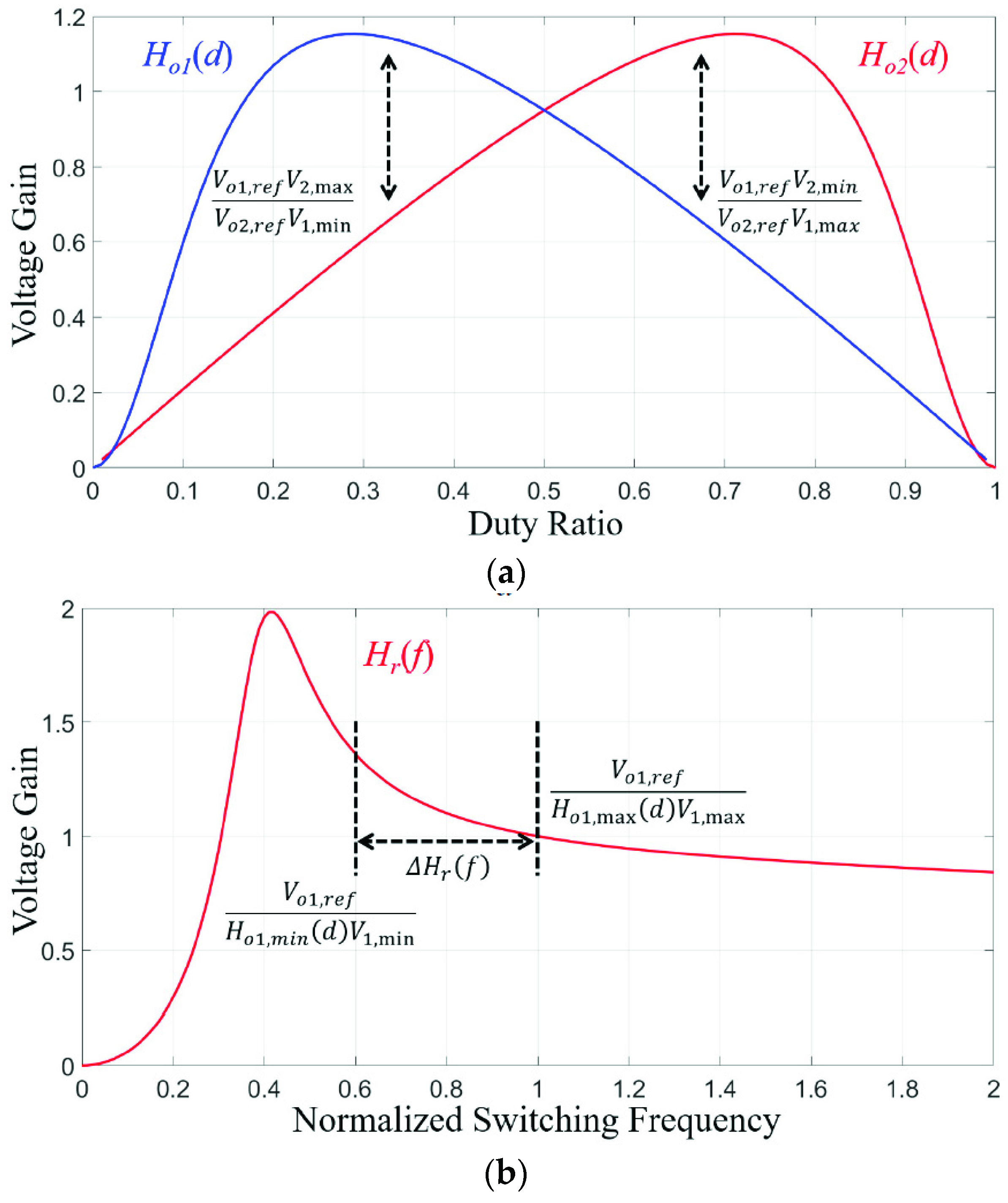
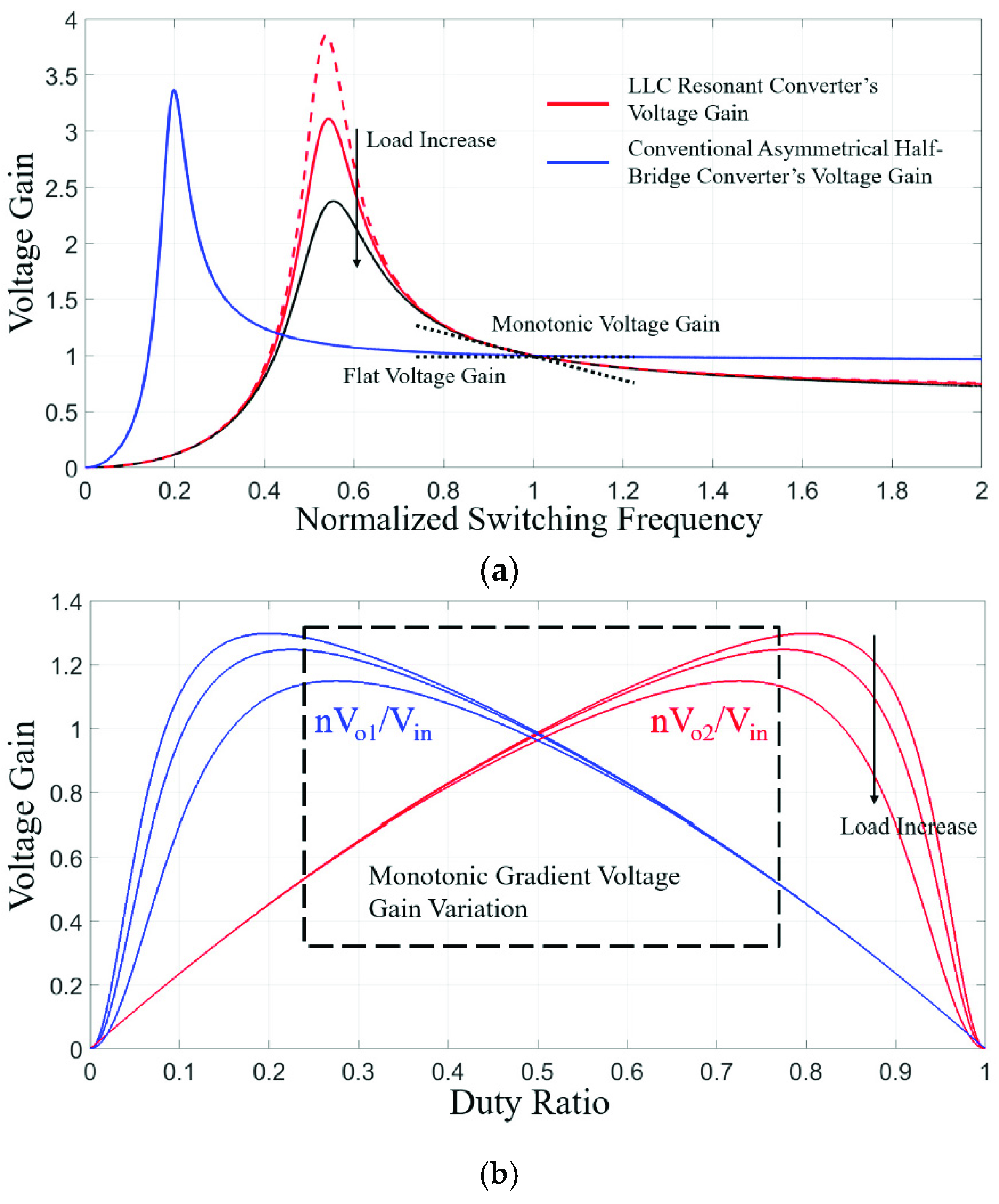
2.2. Gain Analysis According to Modulation Methods

The input-output voltage gain can be derived with the first harmonic approximation (FHA) as follows [29]:
H r ( f n ) = [ ( 1 + k k f n 2 ) 2 + Q 2 ( f n 1 f n ) 2 ] 1 2
where fn is the normalized switching frequency, k is Lr/Lm inductance ratio, and Q is the quality factor as follows:
R o , e = V o , F H A I o , F H A = 8 n 2 π 2 R o ,   f n = f s f r ,   Q = L r C r R o , e ,   k = L r L m
where Ro is the output resistance, fs is the switching frequency, and fr is the resonant frequency.
The conventional asymmetric half-bridge converter, only controlled by the APWM, uses small resonant inductance to obtain the linear voltage gain by the APWM [30]. However, it induces a flat voltage gain by the PFM, which cannot regulate the output voltage with PFM. Therefore, the resonant inductance is high enough to obtain the monotonic voltage gain by the PFM, as shown in Figure 4a. The large resonant inductance has limited monotonic voltage gain by the asymmetric duty variation.
The conventional voltage gain of the APWM can be derived as follows [33]:
V o V i n L m D n ( L m + L r )
where D is the duty ratio. It has validity only for small resonant inductance conditions. Therefore, the voltage gain with enough resonant inductance is required to implement the hybrid control algorithm for the entire load conditions.
In steady state, the offset current on the magnetizing inductance can be derived as follows:
I o f f s e t = I o 1 n 1 I o 2 n 2 = 1 T s 0 T s ( i r ( t ) i m ( t ) ) d t
Assuming that Vcr is constant in Mode 1, Vcr,ini can be derived as follows:
n V o 1 D T s L m = V c r , i n i ( 1 D ) T s L m V c r , i n i = 1 D D n V o 1
From (1), (2) and (6), (7), the proposed input to output voltage gains (Ho1(D) = n1Vo2/Vin, Ho2(D) = n2Vo2/Vin) according to the asymmetric duty ratio can be derived as follows:
n V o 1 V i n = D 1 cos ( A ) Z 1 ω 1 D ω r ( R + D T s 2 L m ) sin ( A ) + D 2 T s ( 1 n 1 2 R o 1 1 n 2 2 R o 2 ) + 1 cos ( A ) Z 1 ω r n V o 2 V i n = D 1 cos ( A ) Z 1 ω 1 D ω r ( R + ( 1 D ) T s 2 L m ) sin ( A ) + D 2 T s R + 1 cos ( A ) Z 1 ω r
where D′ = 1 − D, Z1 = Lr/Cr, R′ = 1/(n12Ro1) − 1/(n22Ro2), A = ωrDTs, and A′ = ωrDTs.
Figure 4b shows the voltage gain of the APWM according to load variations. It shows a complementary voltage gain relationship between Vo1 and Vo2 in the monotonic gradient voltage gain region. From (8), the design of APWM operational range is necessary to obtain the monotonic gradient voltage gain at the designed APWM range.

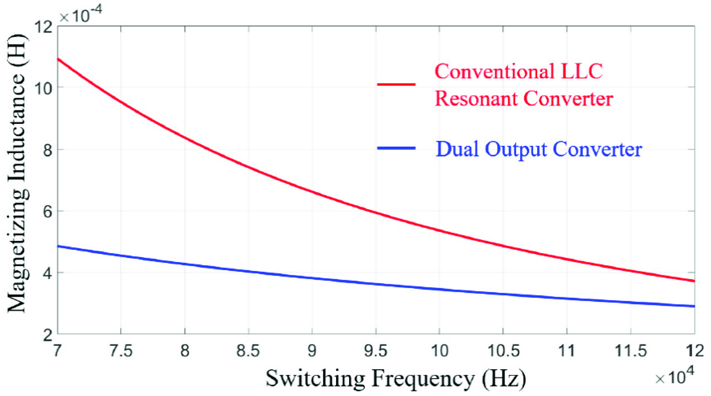
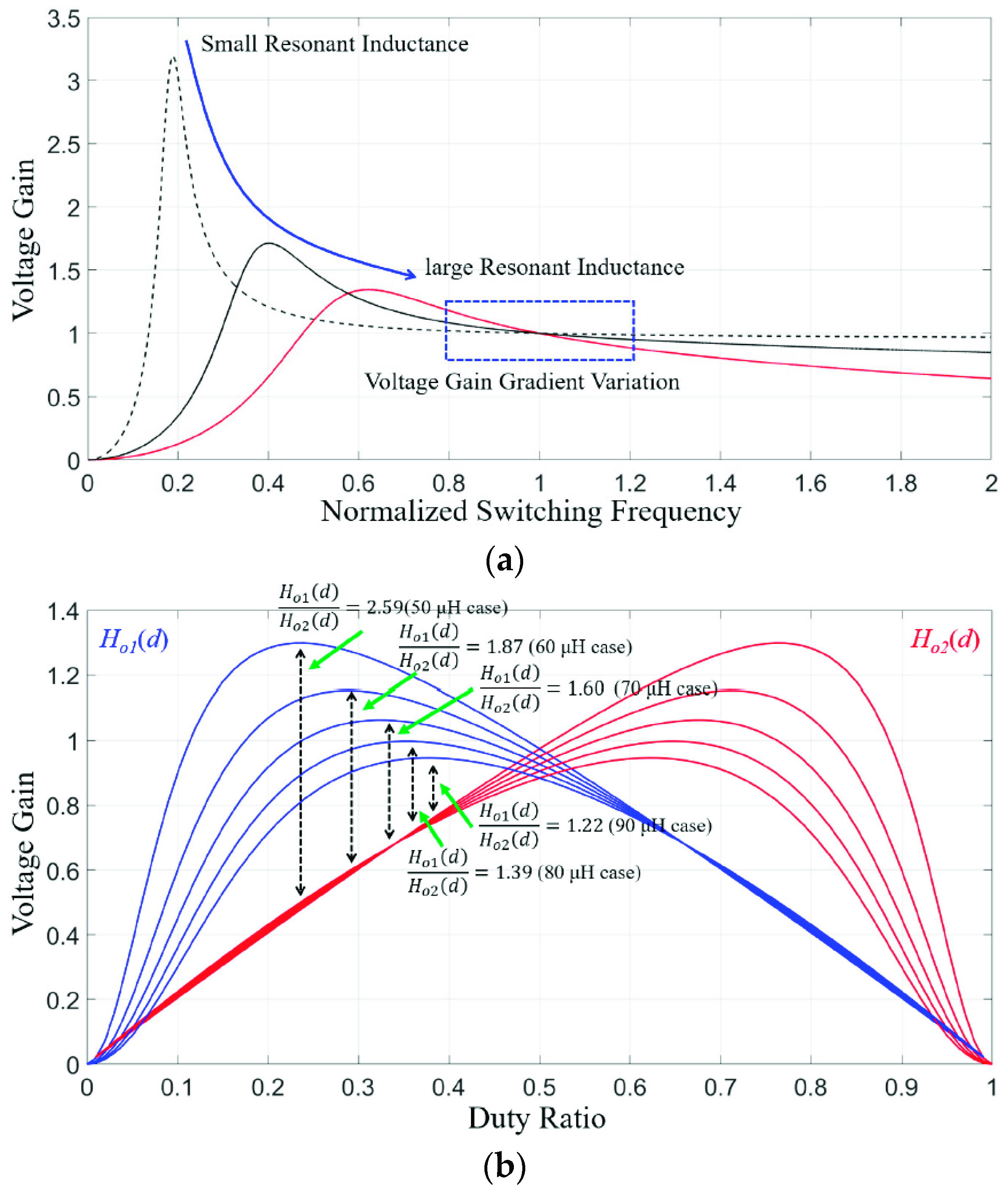
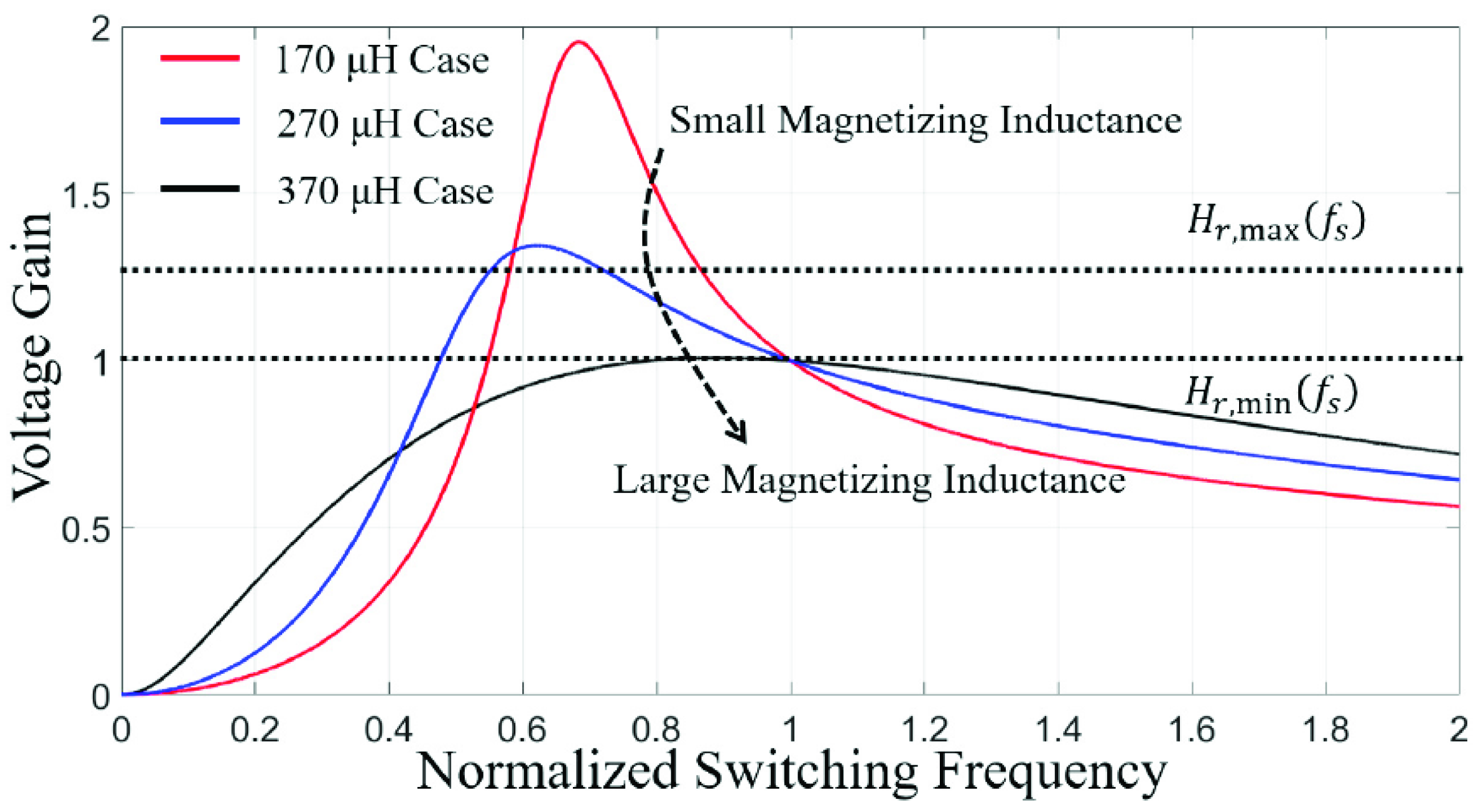
2.3. Magnetizing Inductance Design for Soft Switching Capability

The ZVS capability of the primary MOSFETs is achieved by discharging and charging their output capacitance during the dead time. Therefore, the LLC resonant converter requires enough magnetizing current and dead time duration to guarantee ZVS condition which can be expressed as follows:
i p ( t d t ) i r e q ( t d t )
where ireq (=2VinCs/tdt) is the required minimum primary current to obtain the ZVS condition on the primary MOSFETs, Cs is the equivalent output capacitance of the primary MOSFETs, and tdt is the dead time duration.
From (6), the dual-output LLC resonant converter makes an unbalanced magnetizing current during the dead time based on each load condition of the dual-output. The unbalanced magnetizing current has to satisfy (9) to achieve ZVS operation. Therefore, the design of the magnetizing inductance and the dead time duration should take unbalanced magnetizing currents into consideration. Assuming the primary current is constant during the dead time, the proposed ZVS condition in the dual-output converter can be derived as follows:
t d t 1 ( C s 1 + C s 2 ) V i n | i p ( t c ) | = ( C s 1 + C s 2 ) V i n | I o f f + n 1 V o 1 2 L m D T s | t d t 2 ( C s 1 + C s 2 ) V i n | i p ( t c ) | = ( C s 1 + C s 2 ) V i n | I o f f n 2 V o 2 2 L m ( 1 D ) T s |
where Cs1 and Cs2 are the output capacitance of S1 and S2, respectively, and fs,max is the maximum switching frequency, tdt1 = tdtc and tdt2 = tgtf are the first and second dead time of the primary MOSFETs, respectively. From (10), tdt can be reformulated as follows:
t d t 2 C s V i n min { | i p ( t c ) | , | i p ( t f ) | }
From (10) to (11), the proposed magnetizing inductance for the ZVS capability can be derived as follows:
L m t d t 1 D min T s n 1 V o 1 2 ( C s V i n I o f f , max t d t 1 ) L m t d t 2 ( 1 D max ) T s n 2 V o 2 2 ( C s V i n I o f f , max t d t 2 )
From (11) and (12), the proposed magnetizing inductance and dead time duration can be designed for the dual-output LLC resonant converter to obtain ZVS capability of the primary MOSFETs over the entire load condition. These equations consider both the unbalanced magnetizing current and the switching frequency variation to achieve ZVS. Figure 5 shows the comparison of the required magnetizing inductance between the conventional LLC resonant converter and the dual-output converter to achieve ZVS. The dual-output converter requires lower magnetizing inductance for ZVS capability compared to the conventional LLC resonant converter.

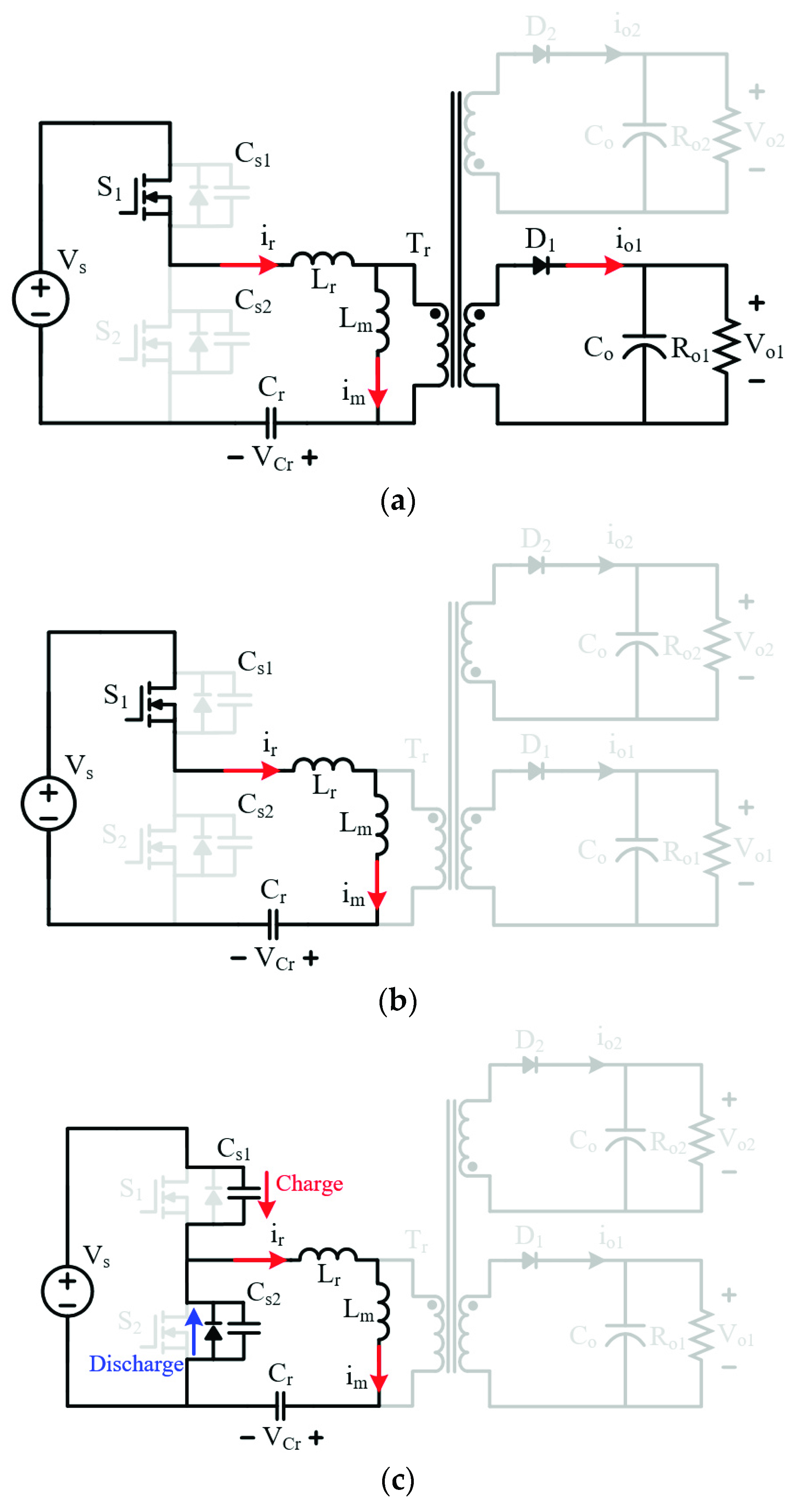
3. Analysis of PFM and APWM Hybrid Control Algorithm and Resonant Tank Design

In this section, the operational principle of the hybrid control algorithm is analyzed to regulate output voltages. Through this analysis, the resonant tank is designed to achieve output voltage error compensation.

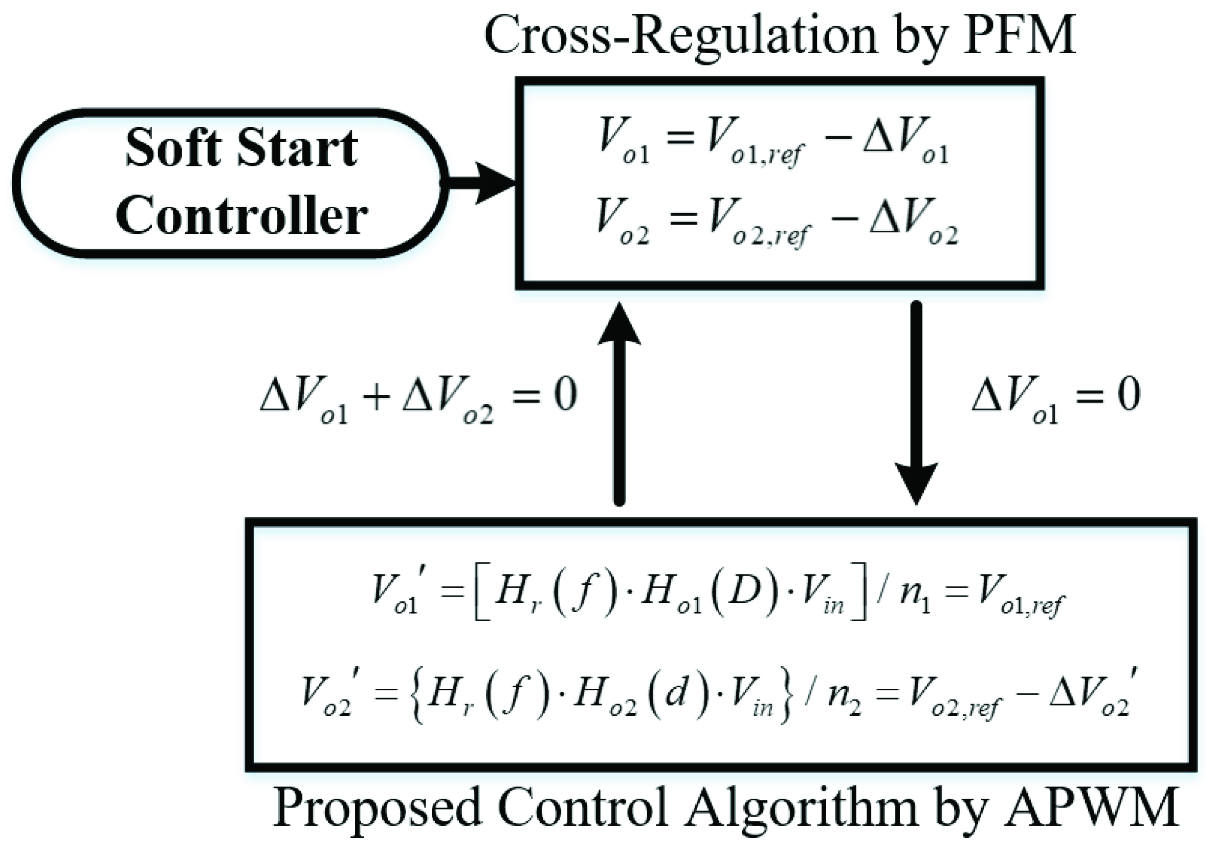
3.1. Analysis of the Hybrid Control Algorithm

The hybrid control algorithm has two control freedoms using two independent modulation methods. The PFM is adapted to regulate the output voltages using the conventional cross regulation method. In steady state, the conventional multiple output feedback can be derived as follows:
k w 1 V o 1 + k w 2 V o 2 = V r e f
where kw1 and kw2 are weight factors and Vref is the reference output voltage. From (13), the output voltage errors using the weight factor can be derived as follows:
k w 1 Δ V o 1 + k w 2 Δ V o 2 = 0 V o 1 = V o 1 , r e f + k w 1 Δ V o 1 V o 2 = V o 2 , r e f + k w 2 Δ V o 2
where Vo1,ref and Vo2,ref are the reference voltages of Vo1 and Vo2, and ΔVo1 and ΔVo2 are output voltage errors of Vo1 and Vo2, respectively. The feedback method for the multiple outputs affects the performance of the cross regulation using the weight factors. As a result, (14) cannot eliminate the output voltage errors which are divided into each output voltage according to the weight factor.
The APWM control method is adopted to regulate Vo1, which makes zero steady state voltage errors of the Vo1 channel. The complementary voltage gain relationship between each output channel also reduces the output voltage error of Vo2, as shown in Figure 4b. The decrement of the Vo1 and Vo2 error using the APWM can be derived as follows:
Δ V o 1 = H o 1 ( D ) V o 1 V o 1 , r e f 0 Δ V o 2 = H o 2 ( D ) V o 2 V o 2 , r e f
where ΔVo1′ and ΔVo2′ are the output voltage errors which are compensated with the APWM control method. The Vo1 error is almost zero after the APWM control, however, the APWM cannot completely compensate the Vo2 error. From (15), the output voltages after the APWM regulation can be derived as follows:
V o 1 = V o 1 , r e f ,   V o 2 , r e f = V o 2 , r e f Δ V o 2
where Vo1′ and Vo2′ are the output voltages of each output channel, which are compensated by the APWM. The flow chart of the hybrid control algorithm is shown in Figure 6 which shows the control sequence of the output voltage regulation to reduce the output voltage errors.
After the APWM regulation, the cross regulation using the PFM with the feedback for the multiple outputs divides the output voltage error of Vo2 with respect to the weight factors as follows:
V o 1 , r e f [ H o 1 ( d ) H r ( f s , c ) V i n ] / n 1 k w 2 Δ V o 2 V o 2 , r e f [ H o 2 ( d ) H r ( f s , c ) V i n ] / n 2 k w 1 Δ V o 2
where fs,c is the switching frequency which divides the output voltage error according to the weight factor, and Hr(fs,c) is the voltage gain of the PFM at the fs,c. The voltage gain according to the switching frequency satisfies (13) to divide the output voltage error with respect to the weight factor. From (17), the output voltages regulated by the PFM can be derived as follows:
V o 1 = V o 1 , r e f k w 2 Δ V o 2 ,   V o 2 , r e f = V o 2 , r e f + k w 1 Δ V o 2
where Vo1″ and Vo2″ are the output voltages of each output channel, which are compensated by the PFM at the next control step. The control iterations of the PFM and the APWM can reduce the output voltage errors of Vo1 and Vo2.
From (15) to (18), the voltage gain variation by the PFM and the APWM can decrease the output voltage error. However, the dual-output converter has limited voltage gain variation caused by the switching frequency and the duty ratio ranges. The proper operating ranges to obtain tightly regulated output voltages can be calculated as follows:
H o 1 ( d ) H r ( f s ) V 1 = V o 1 , r e f H o 2 ( d ) H r ( f s ) V 2 = V o 2 , r e f
where V1 = Vin/n1Io1Reff, V2 = Vin/n2Io2Reff, and Reff is the effective series resistance. The voltage gain variation according to the PFM and the APWM has to satisfy (19) for the tight output voltage regulations. Using (19), the required voltage gain of the APWM can be calculated as follows:
H o 1 ( d ) = V o 1 , r e f V 2 V o 2 , r e f V 1 H o 2 ( d )
From (20), the APWM control method requires a voltage gain difference between Ho1(d) and Ho2(d) to reduce the output voltage error. The maximum voltage gain difference range of the APWM can be derived at the worst load condition as follows:
H o 1 ( d ) H o 2 ( d ) = max ( V o 1 , r e f V 2 , min V o 2 , r e f V 1 , max , V o 1 , r e f V 2 , max V o 2 , r e f V 1 , min )
where V1,max and V1,min are minimum and maximum output voltages of Vo1, respectively, V2,max and V2,min are minimum and maximum output voltages of Vo2, respectively. These consider the voltage drop according to the forward bias and conduction loss. Figure 7a shows the maximum voltage gain difference between Ho1(d) and Ho2(d).
The required voltage gain of the PFM can be obtained for the cross regulation as follows:
H r ( f s ) = V o 1 , r e f H o 1 ( d ) V 1
From (22), the maximum and minimum voltage gains for the cross regulation can be derived as follows:
H r , max ( f s ) = V o 1 , r e f H o 1 , min ( d ) V 1 , min H r , min ( f s ) = V o 1 , r e f H o 1 , max ( d ) V 1 , min
where Ho1,min(d) and Ho1,max(d) are the minimum and maximum voltage gains of the APWM, respectively. Figure 7b describes the maximum and the minimum voltage gains to implement the cross regulation method. The resonant tank should be designed to compensate the maximum output voltage difference of the dual-output converter. The voltage gain according to the duty cycle and the switching frequency should satisfy (21) and (23) to compensate the maximum power difference. The power converter does not require any additional circuits to implement the hybrid control algorithm. Therefore, the power converter size is not affected by the control algorithm.

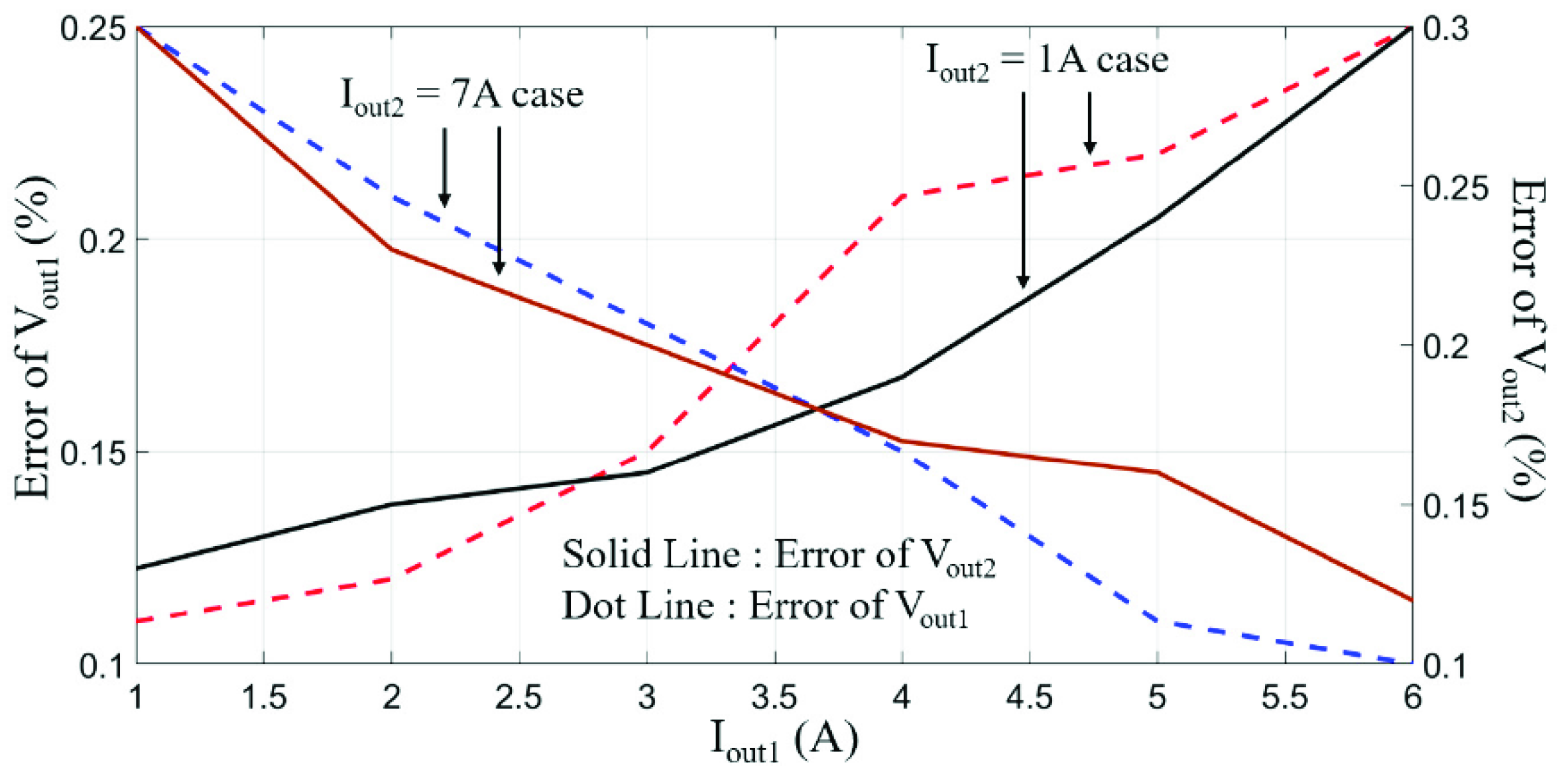
3.2. Resonant Tank Design for Minimizing Output Voltage Error

The voltage gain using APWM and PFM has to satisfy (21) and (23) for compensation of output voltage error over the entire load range. Figure 8 shows the voltage gain variation according to the resonant inductance and the modulation methods. Large resonant inductance makes monotonic voltage gain variation as switching frequency varies around the resonant frequency. However, the large resonant inductance reduces the compensation range according to the APWM by (8). On the other hand, small resonant inductance can compensate the large output voltage error using the APWM according to (5). However, it induces flat voltage gain variation according to the PFM, which makes large switching frequency variation to obtain the proper voltage gain for minimizing the output voltage error. Therefore, the maximum resonant inductance design is required to achieve small switching frequency variation and output voltage error compensation.
The maximum and minimum output voltages can be calculated with loss analysis. The primary side voltage drop can be calculated as follows:
V t r = V i n I p ( R d s + R t r 1 + R c )
where Vtr is the transfer voltage from the primary to the secondary side, Ip is the primary current, Rds is the on resistance of MOSFET, Rtr1 is the primary resistance of the transformer, and Rc is the resistance of the resonant capacitor. In addition, the output voltage can be calculated as follows:
V o 1 = V t r / n V D 1 I o 1 R t r 2 V o 2 = V t r / n V D 2 I o 2 R t r 2
where VD1 and VD2 are the on-drop voltage of secondary diodes, Io1 and Io2 are the secondary rms currents of each output channel, and Rtr2 is the series resistance of the transformer. Table 1 shows the specification of the proposed dual-output LLC resonant converter and its parasitic components.
From (8), (21) and (25), the resonant impedance (Z1) can be designed to compensate the output voltage errors for the entire load range. Within the designed duty variation range, the resonant impedance can be derived as follows:
L r C r = x ( D B ) B ω r ( D B ) B ω r ( D B ) C x ( D B ) C
where x is the maximum voltage gain ratio by (21), B = 1 − cos(A), B′ = 1 − cos(A′), C = (D/ωr)[R′ + (DTs)/2Lm]sin(A′) + D2TsR′, and C′ = (D′/ωr)[R′ + (DTs)/2Lm]sin(A) + D2TsR′. From (26), the resonant inductance and capacitance can be calculated to obtain the tight output voltage regulation.
The design methodology of the resonant tank can be described as follows. First, the specifications, such as input voltage range, resonant frequency, and output voltages, are required to design the power stage. Second, the magnetizing inductance is designed by considering the resonant frequency, the input voltage, and the parasitic capacitance of the MOSFETs, which was derived in (12). Third, the resonant inductance and capacitance ratio can be designed using (26). From the loss analysis, the required maximum voltage gain ratio can be calculated using (21), and (25). Through the proposed design methodology, the dual-output LLC resonant converter can achieve tight output voltage regulation and ZVS capability for the entire load conditions.
The example of the power stage design can be described as follows.
  • Step 1: The design specifications are shown in Table 1.
  • Step 2: The magnetizing inductance can be calculated with (12). The proper magnetizing inductance is 280 μH to achieve ZVS for the entire load range as shown in Figure 9.
  • Step 3: The required maximum voltage gain ratio is 1.31 and 0.64, which can be calculated with (21), and (25). The resonant inductance and capacitance can be calculated with (26), which are 70 μH and 30 nF. Therefore, the design example shows resonant impedance and magnetizing inductance to achieve ZVS for the entire load range, which can compensate all voltage errors of all the outputs using the hybrid control algorithm.

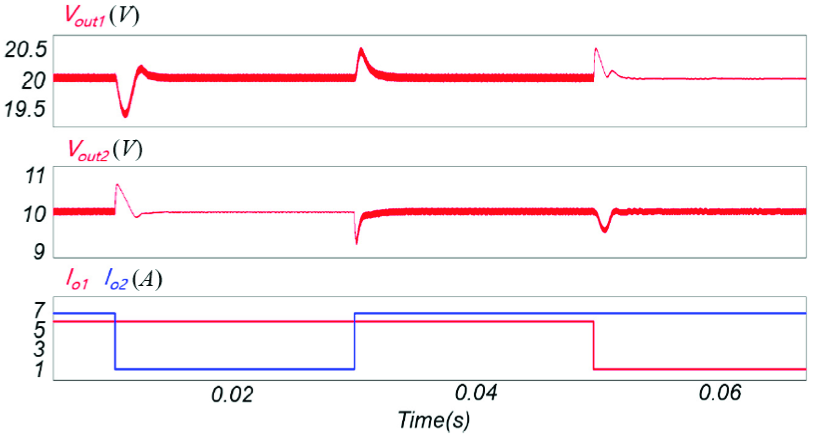
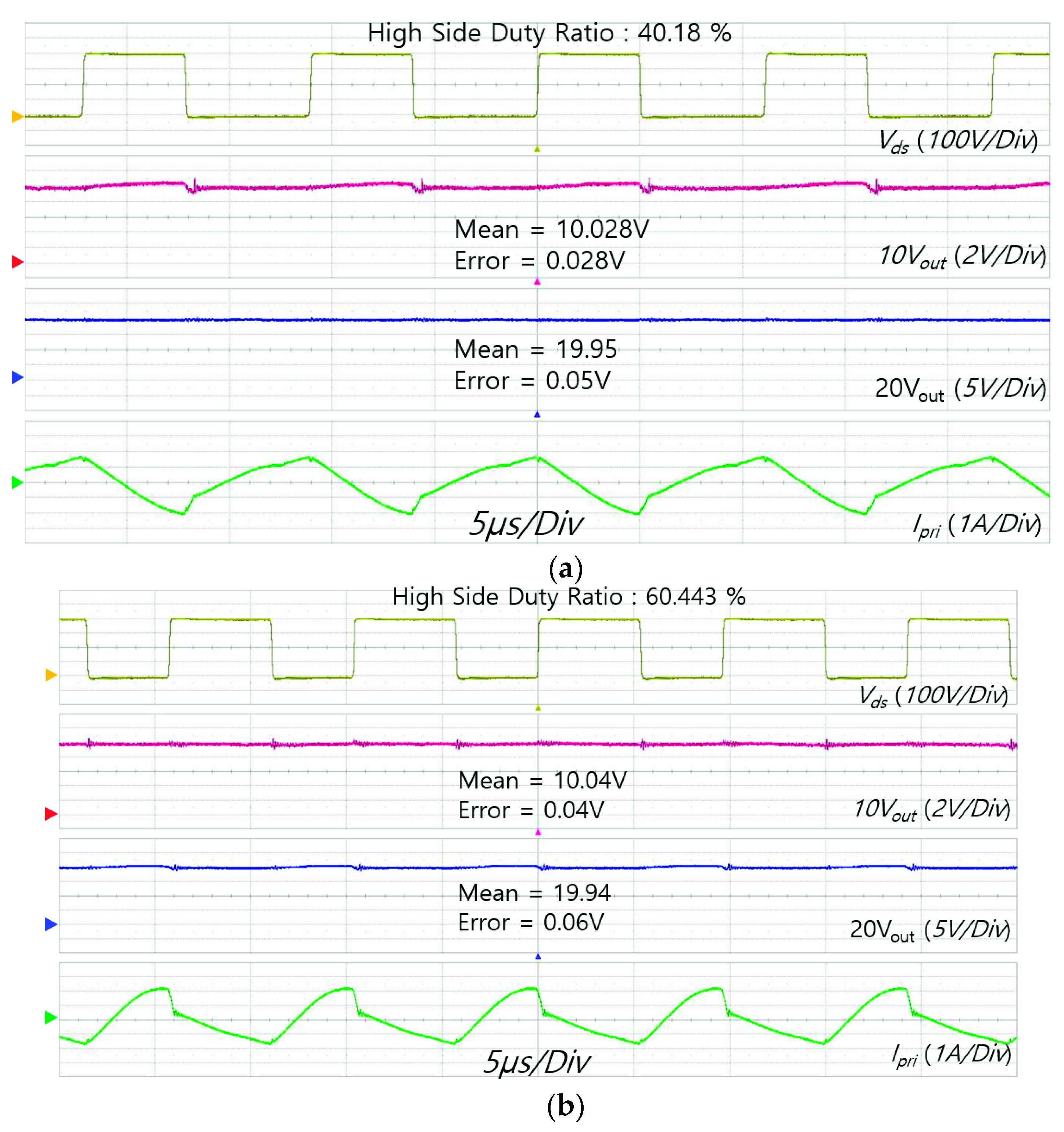
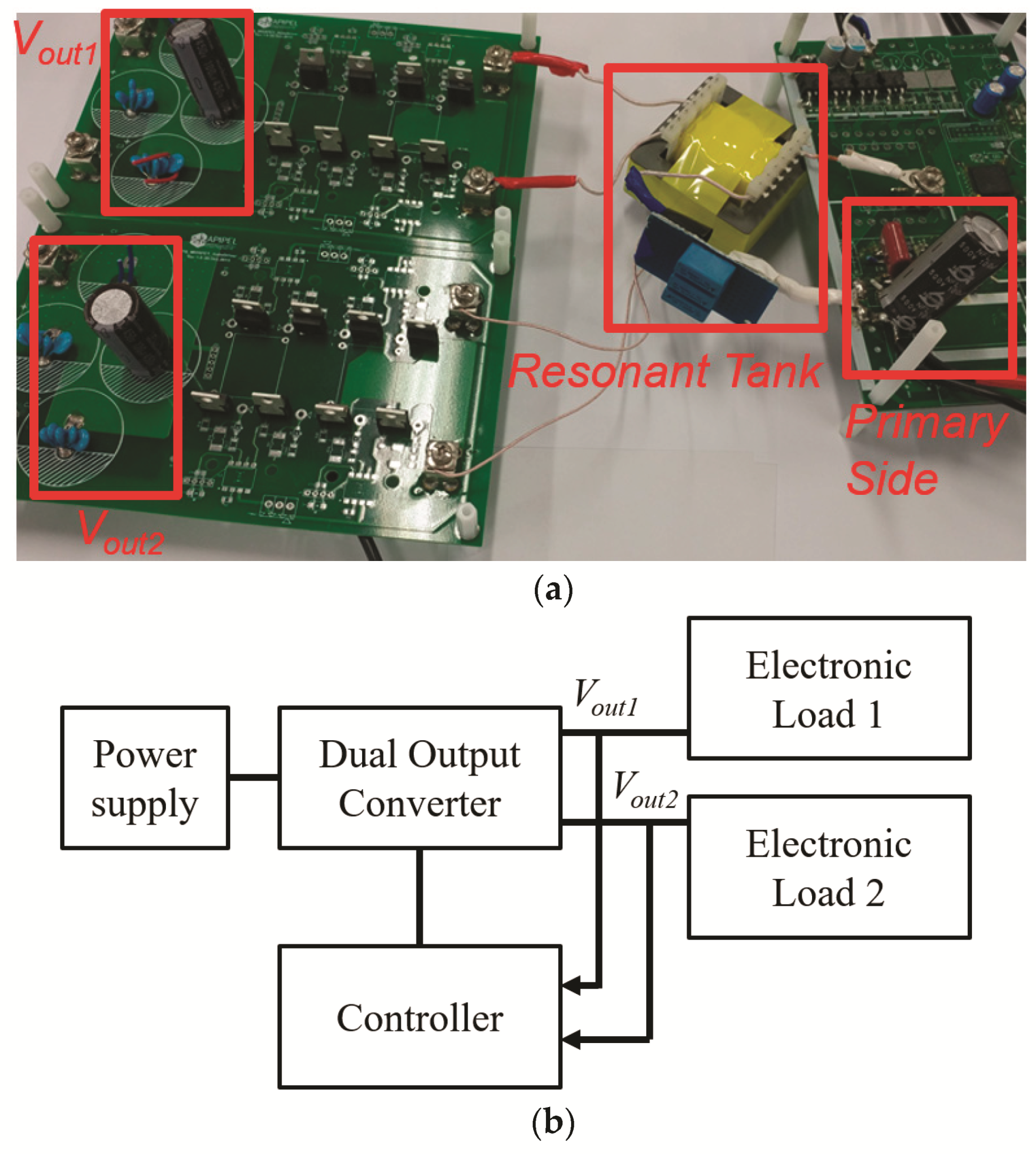
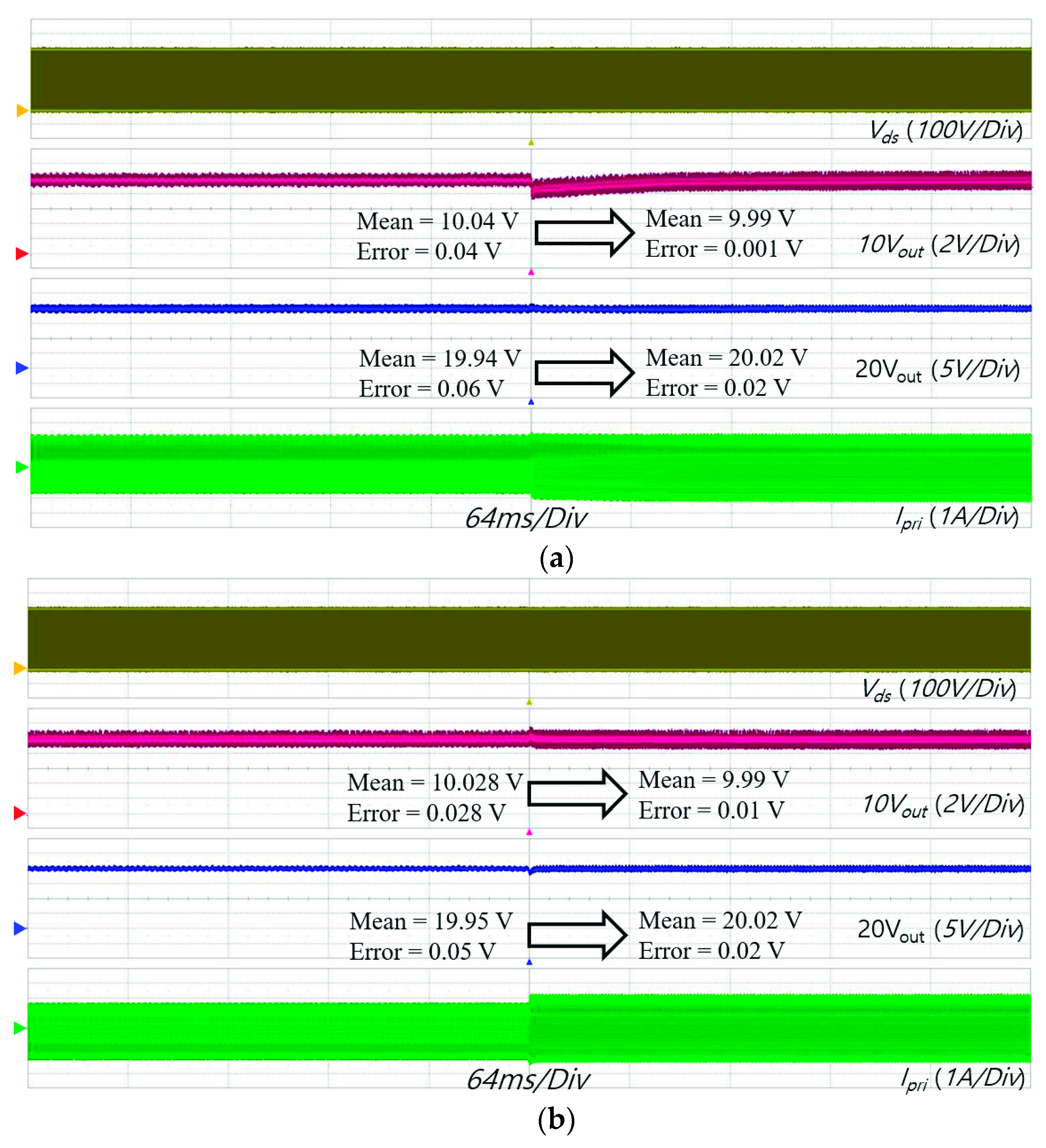
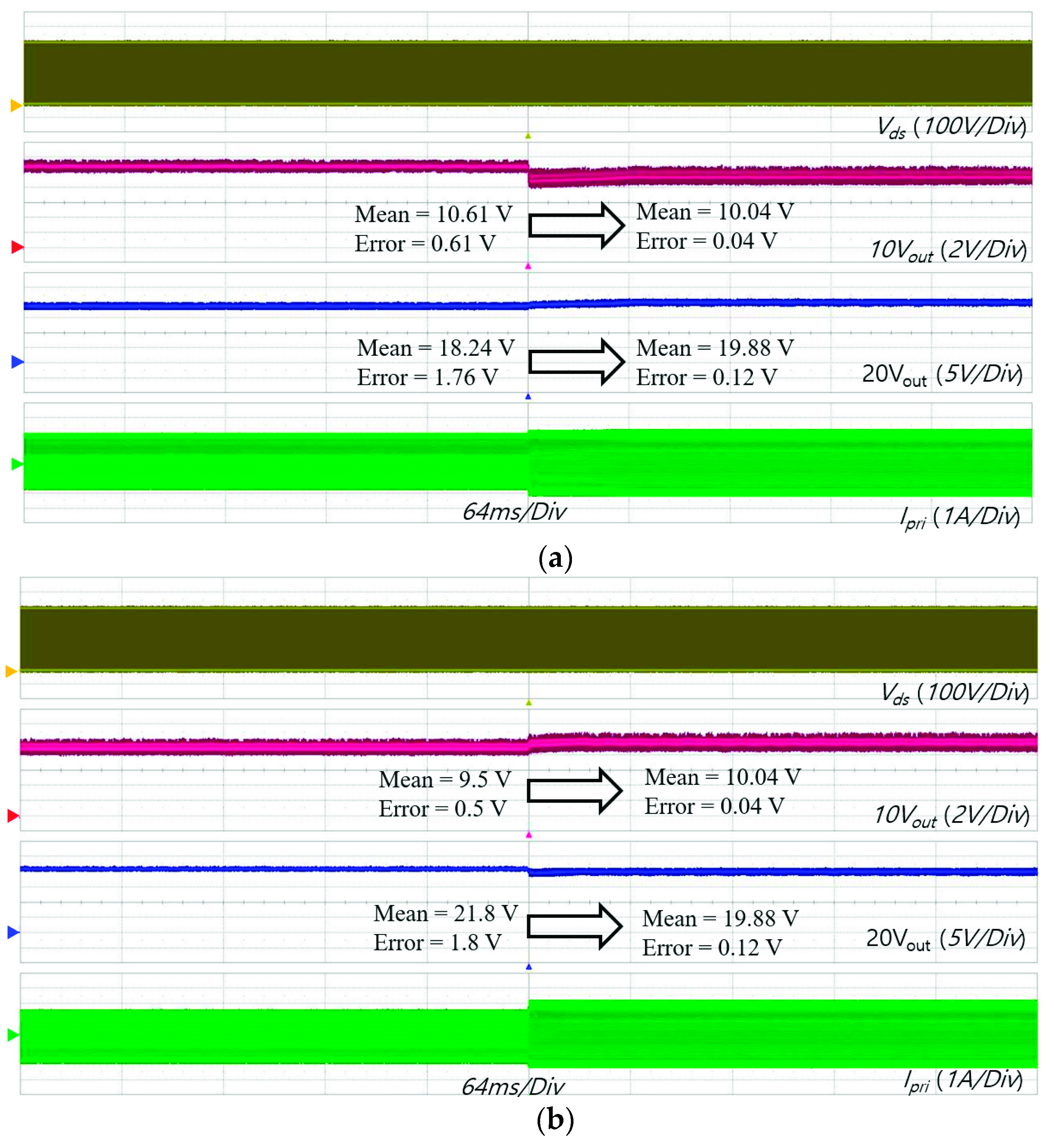
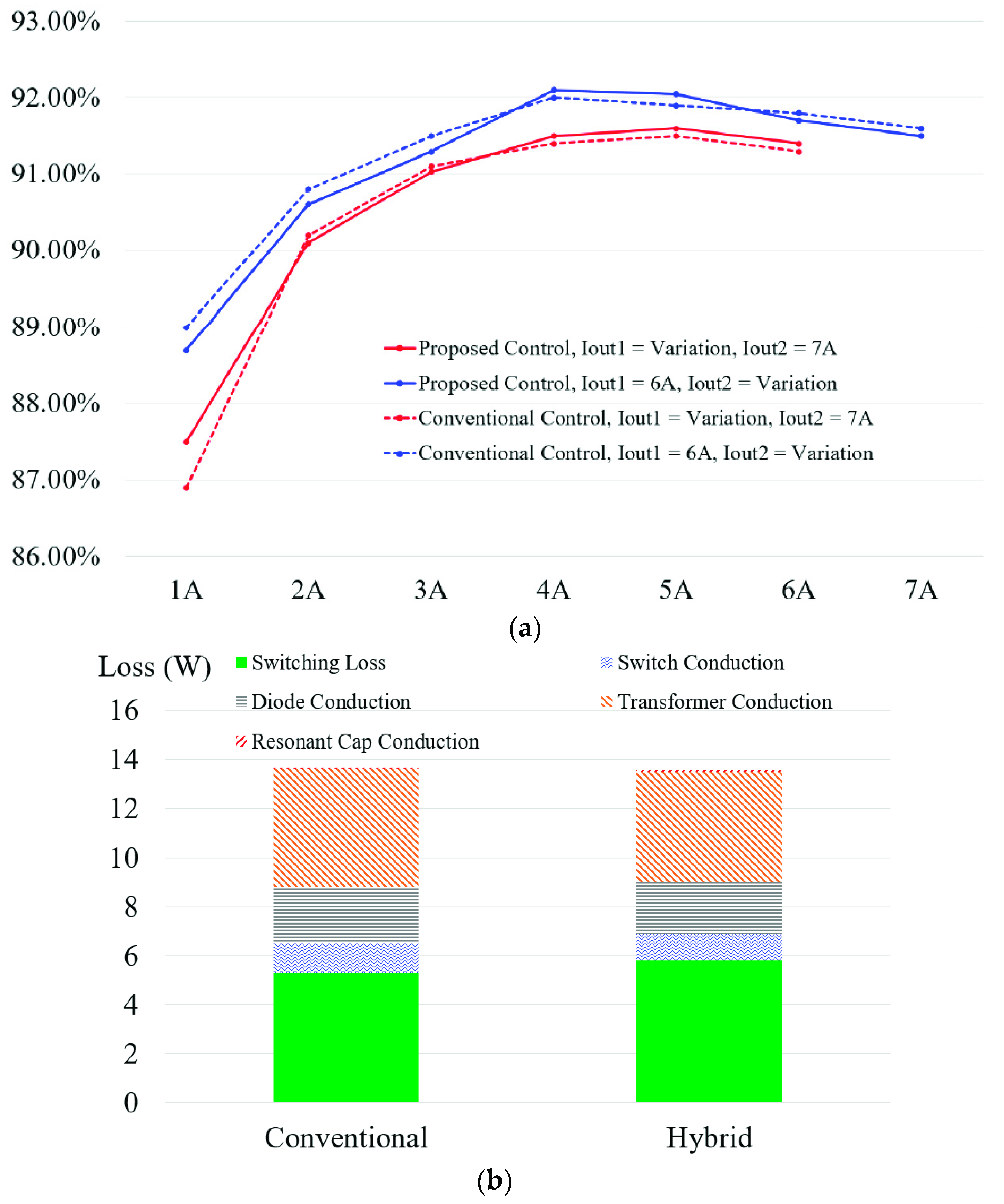
4. Experimental Results

Figure 10 shows the simulation result of the PFM-APWM hybrid control method which has the minimum output voltage error, almost zero, according to the load variation. The simulation results verify the performance enhancement of tightly regulated output voltage of the hybrid control algorithm compared to the conventional cross regulation method. Figure 11 shows the prototype converter and diagram of the experimental setup to verify the performance of the proposed hybrid control algorithm. Figure 11a shows a photograph of the prototype converter which has two outputs and a single primary side. Two separated electronic loads are connected to the converter to verify the output voltage regulation performance as shown in Figure 11b.
The conventional cross regulation method has high output voltage error (6.1% for Vo1 and 9% for Vo2) since its performance is not enough to compensate the output voltage error at the worst load condition. Figure 12 shows experimental waveforms of a prototype dual-output LLC resonant converter using the PFM-APWM hybrid control method at the worst load condition. The proposed control method shows much smaller output voltage error (0.25% for Vo1 and 0.3% for Vo2) than that of the conventional method. It verifies the validity of the proposed design methodology with tight output voltage regulation at the worst load condition. The small voltage error of the hybrid control method might be composed of analog-to-digital conversion (ADC) and measurement errors.
Figure 13 shows the voltage error in cross regulation according to the load variation. In Figure 12, large load difference causes bigger errors of the output voltages. All the detail measured values of the simulation and experimental results are shown in Table 2 which shows the performance comparison of the cross regulation in the output voltages according to the control method. When two output powers are similar, the conventional and hybrid control algorithm has good output voltage regulation performance. When two output powers are significantly different, the conventional control algorithm has poor output voltage regulation. However, the hybrid control algorithm with the proposed design methodology can tightly regulate the output voltage for the entire load difference. The hybrid method shows more than 20 times less voltage regulation errors than those of the conventional simple cross regulation method at the worst condition.
Figure 14 shows the step load response of the prototype dual-output LLC resonant converter using the PFM-APWM hybrid control method which regulates the output voltages under load variations. There are no oscillations and disturbances in the converter operating waveforms. The results indirectly verify operating stability of the dual-output converter controlled by the hybrid control algorithm. Figure 15 shows the step load response of the conventional cross regulation method. The conventional regulation method has poor output voltage regulation according to the load condition. At the worst condition, the output voltage regulation performance is 24 times poorer compared with the hybrid control algorithm. The poor output voltage regulation is shown in Table 2. Figure 16 shows the power conversion efficiency of the prototype converter according to the load variations which show the load change in one output channel when the other is set to a fixed value. The proposed algorithm reduces the offset current on the magnetizing inductance compared with the case of the conventional method. However, the APWM operation induces a higher turn-off loss than that of the conventional method. Figure 16b shows the loss analysis according to the control method. Figure 16a shows the power conversion efficiency between the conventional and proposed methods. The power conversion efficiency is similar between the two control methods.

5. Conclusions

In this paper, the design methodology of a dual-output LLC resonant converter using the PFM-APWM hybrid control method is proposed to obtain tight output voltage regulation and ZVS capability for the entire load conditions. Through the analysis of the operational principle, the magnetizing inductance is designed to obtain ZVS capability. The resonant impedance is designed to implement the tight output voltage regulation for the entire load condition. The simulation and experimental results using the 190 W prototype converter verify the validity of the proposed design methodology, and the hybrid control algorithm. Without any power conversion efficiency degradation, the PFM-APWM hybrid control algorithm reduces the output voltage error to 24.4 times and 30 times smaller than those of the conventional cross regulation method at the worst load condition.

Author Contributions

Conceptualization, H.P., M.K., and J.J.; methodology, H.P.; software, H.P.; validation, H.P., M.K. and J.J.; formal analysis, H.P.; investigation, H.P.; resources, J.J.; data curation, M.K.; writing—original draft preparation, H.P.; writing—review and editing, M.K., J.J., H.K.; visualization, H.P.; supervision, J.J. and H.K.; project administration, J.J.; funding acquisition, J.J.

Funding

This work was supported by the Samsung Research Funding Center of Samsung Electronics under Project Number SRFC-TA1403-51.

Conflicts of Interest

The authors declare no conflict of interest.

References

  1. Xi, Y.; Jain, P.K. A forward converter topology with independently and precisely regulated multiple outputs. IEEE Trans. Power Electron. 2003, 18, 648–658. [Google Scholar]
  2. Chen, Q.; Lee, F.C.; Jovanovic, M.M. Analysis and design of weighted voltage mode control for a multiple-output forward converter. In Proceedings of the Eighth Annual Applied Power Electronics Conference and Exposition, San Diego, CA, USA, 7–11 March 1995; pp. 449–455. [Google Scholar]
  3. Ji, C.; Smith, M.; Smedley, K.M.; King, K. Cross regulation in flyback converters: Analytic model and solution. IEEE Trans. Power Electron. 2001, 16, 231–239. [Google Scholar]
  4. Kim, H.S.; Jung, J.H.; Baek, J.W.; Kim, H.J. Analysis and Design of a Multi output Converter Using Asymmetrical PWM Half-Bridge Flyback Converter Employing a Parallel-Series Transformer. IEEE Trans. Ind. Electron. 2013, 60, 3115–3125. [Google Scholar] [CrossRef]
  5. Kim, J.W.; Ha, J.I. Dual voltage regulation of single switch flyback converter using variable switching frequency. In Proceedings of the IEEE Applied Power Electronics Conference and Exposition (APEC), Long Beach, CA, USA, 20–24 March 2016; pp. 1398–1402. [Google Scholar]
  6. Lo, Y.K.; Yen, S.C.; Song, T.H. Analysis and Design of a Double-Output Series- Resonant DC-DC Converter. IEEE Trans. Power Electron. 2007, 22, 952–959. [Google Scholar] [CrossRef]
  7. Ayachit, A.; Reatti, A.; Kazimierczuk, M.K. Magnetizing inductance of multiple- output flyback dc/dc convertor for discontinuous-conduction mode. IET. Power Electron. 2017, 10, 451–461. [Google Scholar] [CrossRef]
  8. Jung, J.H.; Ahmed, S. Flyback converter with novel active clamp control and secondary side post regulator for low standby power consumption under high efficiency operation. IET Power Electron. 2011, 4, 1058–1067. [Google Scholar] [CrossRef]
  9. Wang, X.; Tian, F.; Batarseh, I. High efficiency parallel post regulator for wide range input dc-dc converter. IEEE Trans. Power Electron. 2008, 23, 852–858. [Google Scholar] [CrossRef]
  10. Kim, J.K.; Lee, J.B.; Moon, G.W. Zero-voltage switching multioutput flyback converter with integrated auxiliary buck converter. IEEE Trans. Power Electron. 2014, 29, 3001–3010. [Google Scholar] [CrossRef]
  11. Kim, E.H.; Lee, J.J.; Kwon, J.M.; Choi, W.Y.; Kwon, B.H. Asymmetrical pwm half-bridge converter with independently regulated multiple outputs. IEEE Proc. Electr. Power Appl. 2006, 153, 14–22. [Google Scholar] [CrossRef]
  12. Su, B.; Wen, H.; Zhang, J.; Lu, Z. A soft-switching post regulator for multi-outputs dual forward dc/dc converter with tight output voltage regulation. IET Power Electron. 2013, 6, 1067–1077. [Google Scholar] [CrossRef]
  13. Park, S.G.; Ryu, S.H.; Cho, K.S.; Lee, B.K. An improved single switched post regulator for multiple output isolated converters. In Proceedings of the IEEE Power Electronics Conference (ECCE), Seoul, Korea, 1–5 June 2015; pp. 2403–2408. [Google Scholar]
  14. Kim, J.K.; Choi, S.W.; Kim, C.E.; Moon, G.W. A new standby structure using multi output full-bridge converter integrating flyback converter. IEEE Trans. Ind. Electron. 2011, 58, 4763–4767. [Google Scholar] [CrossRef]
  15. Hwu, K.I.; Ziang, W.Z.; Kim, C.E.; Moon, G.W. Time-sharing pwm control scheme for isolated multi-output dcdc converter. Electron. Lett. 2015, 51, 1446–1447. [Google Scholar] [CrossRef]
  16. Nami, A.; Zare, F.; Ghosh, A.; Blaabjerg, F. Multi-output dc-dc converters based on diode-clamped converters configuration: Topology and control strategy. IET Power Electron. 2010, 3, 197–208. [Google Scholar] [CrossRef]
  17. Ray, O.; Josyula, A.P.; Mishra, S.; Joshi, A. Integrated dual-output converter. IEEE Trans. Ind. Electron. 2015, 62, 371–382. [Google Scholar] [CrossRef]
  18. Trevisan, D.; Mattavelli, P.; Tenti, P. Digital control of single inductor multiple output step-down dc-dc converters in ccm. IEEE Trans. Ind. Electron. 2008, 55, 3476–3483. [Google Scholar] [CrossRef]
  19. Wang, B.; Kanamarlapudi, V.R.K.; Xian, L.; Peng, K.T.T.X.; So, P.L. Model predictive voltage control for single-inductor multiple-output dcdc converter with reduced cross regulation. IEEE Trans. Ind. Electron. 2016, 63, 4187–4197. [Google Scholar] [CrossRef]
  20. Chen, Y.T.; Shih, F.Y. New multi-output switching converters with mosfet-rectifier post regulators. IEEE Trans. Ind. Electron. 1998, 45, 609–616. [Google Scholar] [CrossRef]
  21. Park, H.; Jung, J. PWM and PFM Hybrid Control Method for LLC Resonant Converters in High Switching Frequency Operation. IEEE Trans. Ind. Electron. 2017, 64, 253–263. [Google Scholar] [CrossRef]
  22. Park, H.; Jung, J. Power Stage and Feedback Loop Design for LLC Resonant Converter in High-Switching-Frequency Operation. IEEE Trans. Power Electron. 2017, 32, 7770–7782. [Google Scholar] [CrossRef]
  23. Choi, Y.-J.; Cha, H.-R.; Jung, S.-M.; Kim, R.-Y. An Integrated Current-Voltage Compensator Design Method for Stable Constant Voltage and Current Source Operation of LLC Resonant Converters. Energies 2018, 11, 1325. [Google Scholar] [CrossRef]
  24. Liu, Y.-C.; Chen, C.; Chen, K.-D.; Syu, Y.-L.; Tsai, M.-C. High-Frequency LLC Resonant Converter with GaN Devices and Integrated Magnetics. Energies 2019, 12, 1781. [Google Scholar] [CrossRef]
  25. Demirel, I.; Erkmen, B. A very low-profile dual output llc resonant converter for lcd/led tv applications. IEEE Trans. Power Electron. 2014, 29, 3514–3524. [Google Scholar] [CrossRef]
  26. Roes, M.G.L.; Duarte, J.L.; Hendrix, M.A.M. Disturbance observer-based control of a dual-output llc converter for solid-state lighting applications. IEEE Trans. Power Electron. 2011, 26, 2018–2027. [Google Scholar] [CrossRef]
  27. Cho, S.H.; Kim, C.S.; Han, S.K. High-efficiency and low cost tightly regulated dual-output llc resonant converter. IEEE Trans. Ind. Electron. 2012, 59, 2982–2991. [Google Scholar] [CrossRef]
  28. Hang, L.; Wang, S.; Gu, Y.; Yao, W.; Lu, Z. High cross-regulation multioutput llc series resonant converter with magamp postregulator. IEEE Trans. Ind. Electron. 2011, 58, 3905–3913. [Google Scholar] [CrossRef]
  29. Wu, H.; Wan, K.; Sun, K.; Xing, Y. A high step-down multiple output converter with wide input voltage range based on quasi two stage architecture and dual output llc resonant converter. IEEE Trans. Power Electron. 2015, 30, 1793–1796. [Google Scholar] [CrossRef]
  30. Elferich, R.; Duerbaum, T. A new load resonant dual-output converter. In Proceedings of the IEEE Power Electronics Conference (ECCE), Cairns, Australia, 23–27 June 2002; pp. 1319–1324. [Google Scholar]
  31. Park, H.; Kim, M.; Jung, J. Tightly regulated dual-output half-bridge converter using PFM-APWM hybrid control method. In Proceedings of the IEEE Applied Power Electronics Conference and Exposition (APEC), Tampa, FL, USA, 26–30 March 2017; pp. 2022–2026. [Google Scholar]
  32. Yang, B.; Lee, F.C.; Zhang, A.J.; Huang, G. LLC resonant converter for front end DC/DC conversion. In Proceedings of the IEEE Applied Power Electronics Conference and Exposition (APEC), Dallas, TX, USA, 10–14 March 2002; pp. 1108–1112. [Google Scholar]
  33. Jung, J.H. Feed-forward compensator of operating frequency for apwm hb flyback converter. IEEE Trans. Power Electron. 2012, 27, 211–223. [Google Scholar] [CrossRef]
Figure 1. Schematic of the dual-output LLC resonant converter.
Energies 12 02146 g001
Figure 2. Operation mode of the dual-output LLC resonant converter: (a) Mode 1, (b) Mode 2, (c) Mode 3.
Energies 12 02146 g002
Figure 3. Operation mode of the dual-output LLC resonant converter: (a) Case A, (b) Case B, (c) Case C.
Energies 12 02146 g003
Figure 4. Voltage gain curves: (a) According to normalized switching frequency, (b) according to asymmetric duty ratio and load variation.
Energies 12 02146 g004
Figure 5. Magnetizing inductance according to the switching frequency for zero voltage switching (ZVS) capability.
Energies 12 02146 g005
Figure 6. Block diagram of the PFM-APWM hybrid control algorithm.
Energies 12 02146 g006
Figure 7. Required minimum and maximum voltage gains: (a) APWM case, (b) PFM case.
Energies 12 02146 g007
Figure 8. Voltage gain variation according to the resonant inductance: (a) PFM case, (b) APWM case.
Energies 12 02146 g008
Figure 9. Compensation range of the output voltage error according to the resonant inductance.
Energies 12 02146 g009
Figure 10. Simulation result using dual-output LLC converter with hybrid control algorithm.
Energies 12 02146 g010
Figure 11. Experimental condition: (a) Prototype converter, (b) diagram of experimental setup.
Energies 12 02146 g011
Figure 12. Experimental waveforms of the output voltage regulation with hybrid control algorithm: (a) Iout1 = 1 A and Iout2 = 7 A, (b) Iout1 = 6 A and Iout2 = 1 A.
Energies 12 02146 g012
Figure 13. Error of output voltages according to the load variation.
Energies 12 02146 g013
Figure 14. Step load responses of the dual-output converter with hybrid control algorithm: (a) Iout1 = 6 A and Iout2 changed from 1 A to 7 A, (b) Iout1 changed from 1 A to 6 A and Iout2 = 7 A.
Energies 12 02146 g014
Figure 15. Step load responses of the dual-output converter with conventional cross regulation method: (a) Iout1 = 6 A and Iout2 changed from 1 A to 7 A, (b) Iout1 changed from 1 A to 6 A and Iout2 = 7 A.
Energies 12 02146 g015
Figure 16. Comparison of power conversion efficiency and loss according to the control algorithm: (a) Power conversion efficiency, (b) loss analysis.
Energies 12 02146 g016
Table 1. Power stage specifications and design parameters of the dual-output LLC resonant converter.
ParameterValueParameterValueParameterValue
Vin400 VLoad 120 V, 6 ALoad 210 V, 7 A
nmod12Lm380 μHLr70 μH
Cr30 nFfr109 kHzRds330 mΩ
Rtr1300 mΩRtr2130 mΩRc40 mΩ
VD1,20.4 V
Table 2. Performance comparison by experimental verifications.
Conventional Cross RegulationProposed Cross Regulation
kw Dutykw1 = 1 and kw2 = 1
D = 1
kw1 = 1 and kw2 = 1
0.35 < D < 0.65
Case 1 ErrorIout1 = 1 A and Iout2 = 7 A
Vout1 = 5% and Vout2 = 9%Vout1 = 0.25% and Vout2 = 0.3%
Case 2 ErrorIout1 = 6 A and Iout2 = 1 A
Vout1 = 6.1% and Vout2 = 8.8%Vout1 = 0.3% and Vout2 = 0.3%
Case 3 ErrorIout1 = 1 A and Iout2 = 1 A
Vout1 = 0.25% and Vout2 = 0.34%Vout1 = 0.12% and Vout2 = 0.18%
Case 4 ErrorIout1 = 6 A and Iout2 = 7 A
Vout1 = 0.41% and Vout2 = 0.63%Vout1 = 0.1% and Vout2 = 0.12%

