Article

Analysis to Input Current Zero Crossing Distortion of Bridgeless Rectifier Operating under Different Power Factors

1
School of Mechanical electronic & Information Engineering, China University of Mining & Technology, Beijing 100083, China
2
School of Mining Engineering Taiyuan University of Technology, Taiyuan 030024, China
*
Author to whom correspondence should be addressed.
Energies 2018, 11(9), 2447; https://doi.org/10.3390/en11092447
Submission received: 23 August 2018 / Revised: 6 September 2018 / Accepted: 12 September 2018 / Published: 14 September 2018
(This article belongs to the Section F: Electrical Engineering)

Abstract

:
The principles and operating characteristics of bridgeless rectifiers under different power factors are discussed with emphasis on analyzing the input current distortion. Firstly, two driving modes are analyzed and compared. Based on the results of comparison it is concluded that the complementary drive mode is a better choice in terms of reducing the current distortion when bridgeless rectifier operates on non-unity power factor. Then, the mechanism causing input current zero-crossing distortion is analyzed. The input current during the distortion is expressed by the piecewise function when a bridgeless rectifier operates under complementary drive mode. Based on the piecewise function, the harmonic analysis is performed. Besides, the relationships between the input current Total Harmonic Distortion (THD) and the filtering inductance, the input current amplitude and the power factor angle are also investigated, which is useful when designing bridgeless rectifiers and selecting the corresponding parameters. Finally, the accuracy of the theoretical analysis is verified through the simulation and experiment.

1. Introduction

Devices based on full-control Pulse Width Modulation (PWM) converter technology have been widely used to solve power quality problems, such as harmonic and reactive power contamination, which is caused by certain power electronic devices. Among them, the static var generator (SVG), static synchronous compensator (STATCOM), and active power filter (APF) are most popularly used in this area [1,2,3]. However, adding these devices into the grid undoubtedly increases the use of physical devices and extra power loss [4]. Therefore, increasing attention is being paid to the incorporation of reactive power compensation and other power quality functionality into fully controlled bidirectional converters used in renewable energy-based generation systems or Vehicle-to-grid (V2G) systems [5,6,7].
However, in many practical applications, including speed regulation with fan type loads, wind power integration, and plug-in electrical vehicle applications, only unidirectional power flow is required. In these situations, some fully controlled switches can be eliminated or replaced to simplify the system, which greatly reduces the complexity of system, saves costs, and improves the system reliability [8,9]. Taking these considerations into account, many researchers have investigated the possibility of incorporating reactive power compensation (RPC) and harmonic current compensation (HCC) functionalities into general unidirectional power converters [10,11].
Bridgeless rectifiers, as a kind of unidirectional converter, have a simpler structure and lower power losses [12,13,14]. Especially when multilevel medium- or high-voltage converters are formed by cascading bridgeless rectifiers, the advantages of fewer massive fully control switching devices, lower costs, and improved reliability become more significant. In [15], a cascaded bridgeless rectifier typology was proposed and a mechanism causing current zero-crossing distortion was discussed. However, a detailed theoretical analysis of the current distortion was not carried out, and the ability of bridgeless rectifiers operating under leading or lagging power factors was not mentioned. The input current distortion of bridgeless rectifiers under a unity power factor was analyzed theoretically in [16] and a control strategy based on specific lagging power factor was proposed, but there was no analysis of the input current distortion under leading or lagging power factor. In [17], some reactive power compensation functionality was integrated in bridgeless rectifiers, and the input current distortion characteristics given different power factors was analyzed to determine the reactive power compensation ability of bridgeless rectifiers. However, all analyses provided by [17] are based on the assumption that bridgeless rectifiers operate under synchronous driving mode. It will be seen from the later discussion that compared with synchronous driving mode, complementary driving mode induces fewer harmonics in the input current of bridgeless rectifiers, and therefore is a more suitable driving mode for bridgeless rectifiers under different power factors.
As mentioned above, the research of bridgeless rectifiers in most literature was performed based on the unity power factor. Only a few studies discuss the characteristics of bridgeless rectifiers operating under non-unity power factors. However, no studies have reported the effect of different driving modes on input current distortion when bridgeless rectifiers operate under non-unit power factors. In order to more effectively integrate RPC and HCC capabilities into a bridgeless rectifier, the harmonic characteristics of bridgeless rectifiers under different power factors in complementary driving mode are discussed in this paper. We concluded that the complementary drive mode is a better choice in terms of reducing the current distortion when bridgeless rectifiers operate under non-unity power factors. Meanwhile, this analysis is helpful for the design of bridgeless rectifiers and the selection of the corresponding parameters under non-unity power factors. Two driving modes for switches are discussed on the basis of the principle of bridgeless rectifiers in Section 2. Then, the characteristics of current zero-crossing distortion under different power factors are analyzed in Section 3. The limitation of filter inductance, input current amplitude, and the value of the power factor angle in the allowable range of the total harmonic distortion (THD) of the current are analyzed in Section 4. Finally, the accuracy of the proposed theoretical analysis is verified through simulation and experiment.

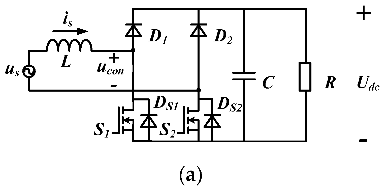
2. Operating Principle and Driving Modes of Switches

2.1. Effective Operation Mode and Mathematical Model

The circuit topology of a bridgeless rectifier is shown in Figure 1a, where ucon is the alternating current (AC) side voltage of bridgeless rectifier and is is the input current. The polarity of ucon and is shown in Figure 1a is defined as positive polarity. L is the AC side filter inductance, C is the direct current (DC) side of the filter capacitor, Udc is the DC side output voltage, and R is the equivalent load of bridgeless rectifier.
Due to the unidirectional conduction property of the fast recovery diodes, the value of the AC side voltage ucon of the bridgeless rectifier depends on the switching state and the polarity of the input current. Thus, there are only four effective operation modes for bridgeless rectifiers as shown in Figure 1b–e, which are summarized in Table 1.
From Table 1, the expression of AC side voltage is obtained as:
u c o n = sgn ( i s ) S U d c
where S (S = 0, 1) refers to the switch function of bridgeless rectifier and sgn ( i s ) is the sign function. If i s 0 , sgn ( i s ) = 1 . If i s < 0 , sgn ( i s ) = 1 .
Applying the Kirchhoff’s voltage law (KVL) and Kirchhoff’s circuit laws (KCL) to the topology shown in Figure 1, the steady-state mathematical model of the system can be obtained by ignoring AC-side power loss:
{ L d i s d t = u s sgn ( i s ) S U d c C d U d c d t = sgn ( i s ) S i s U d c R

2.2. Driving Mode of Two Switches

Since only one switch affects the commutation process during each half cycle of the input current and the two switches have the same source (or emitter) voltage, synchronous and complementary driving modes can be applied.
Figure 2 depicts a block diagram for complementary drive. The output of voltage regulator is shifted to satisfy the required power factor and then given as the input current. Complementary signal gS1, gS2 is generated in modulation as driving signals of switches S1, S2, respectively.
The block diagram for a synchronous drive is shown in Figure 3, where S1 and S2 are driven by the same control signal. However, it is necessary to take the absolute value of the grid voltage and the input current, otherwise the current will be discontinuous in the negative half cycle. The corresponding waveform is shown in Figure 4. Its relevant parameters were selected as Usm = 311 V, f = 50 Hz, Udc = 400 V, R = 0.09 Ω, and L = 3 mH. When the polarity of is reverses from positive to negative, us also reverses its polarity. At this moment, if S1 and S2 are turned on, is runs through S2 and DS1 and increases, while its polarity is negative. When S1 and S2 are turned off, ucon = –udc, based on the boost characteristics of the rectifier, the voltage of the inductance drops, uL = us – ucon > 0. Thus, the polarity of is is negative and the amplitude decreases, which causes i s * i s to become smaller. The duty ratio dS1 of S1 and dS2 of S2 decreases as well. This control leads is in the cut-off state at the negative half cycle.
Synchronous driving mode significantly simplifies the implementation of the control circuit of the bridgeless rectifier and is more popularly used than complementary driving mode in practical applications. When a bridgeless rectifier operates under a unity power factor, there is no difference in the current distortion under the two different driving modes. However, when incorporating the reactive power compensation (RPC) and harmonic current compensation (HCC) functionalities into the bridgeless rectifier, the bridgeless rectifier is required to operate under non-unity power factors. In this situation, the two driving modes have different effects on the input current waveform. It will be seen that complementary driving mode is a better choice in terms of reducing the current distortion compared with synchronous driving, which is discussed in detail in Section 3.

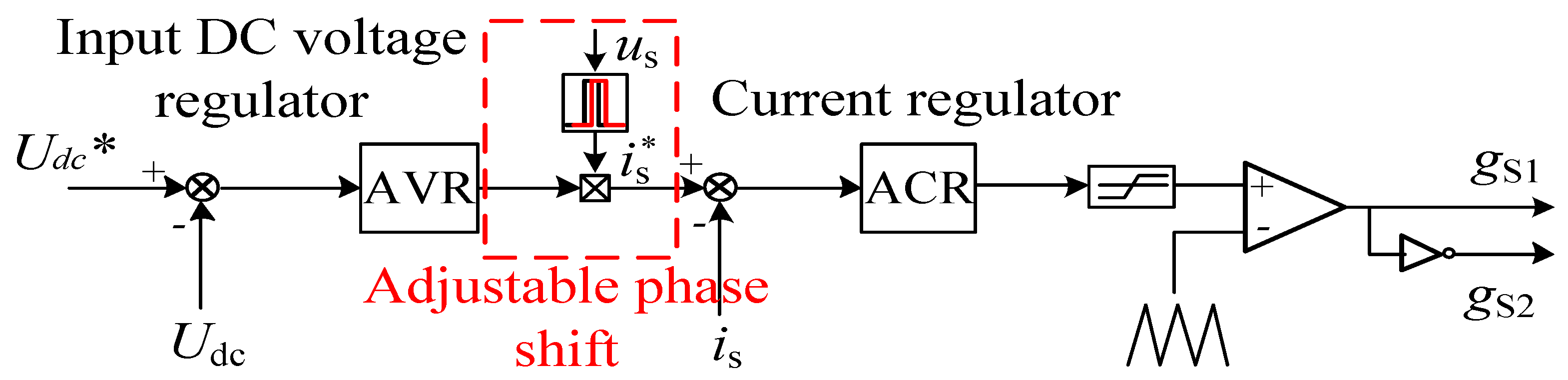
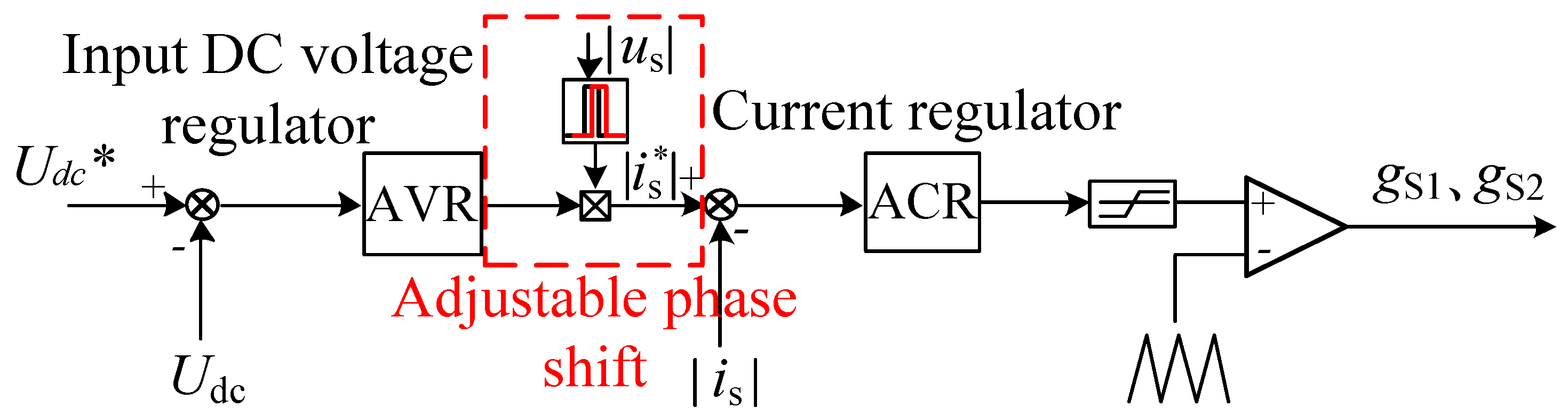
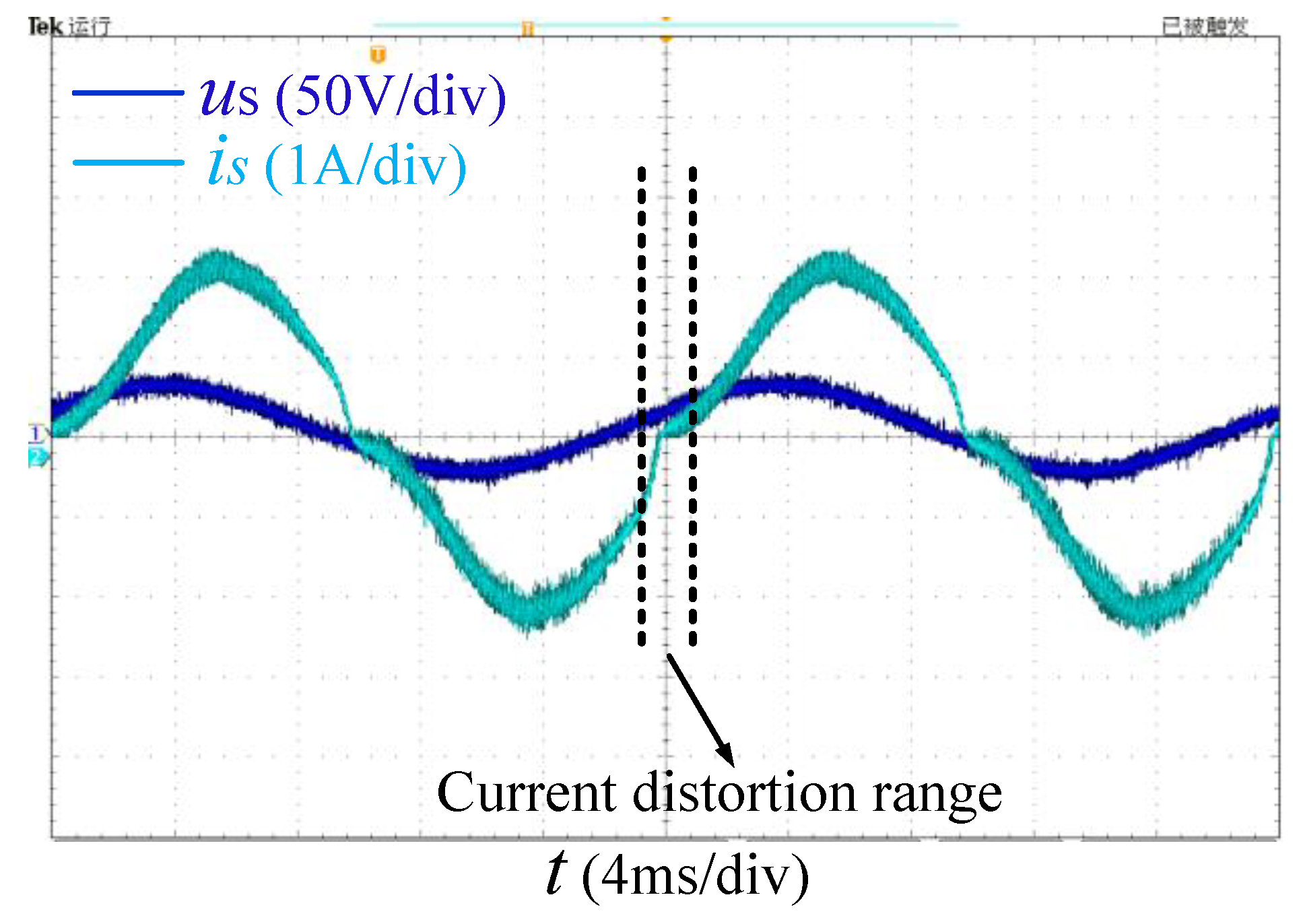
3. Analysis of Input Current Zero-Crossing Distortion

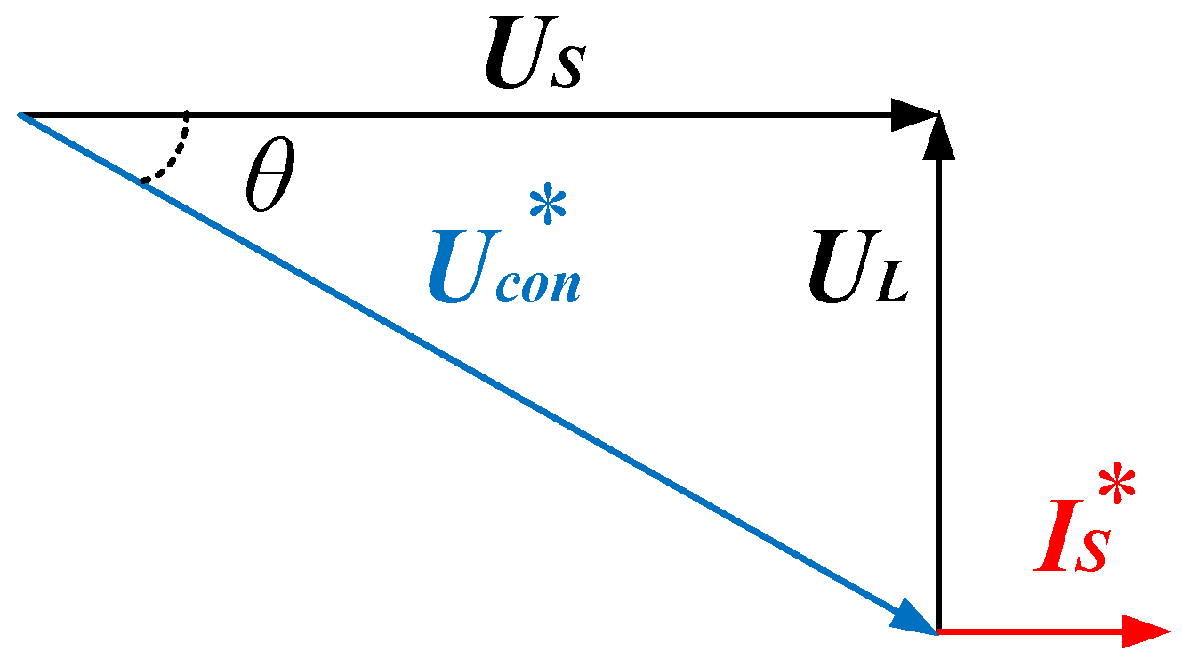
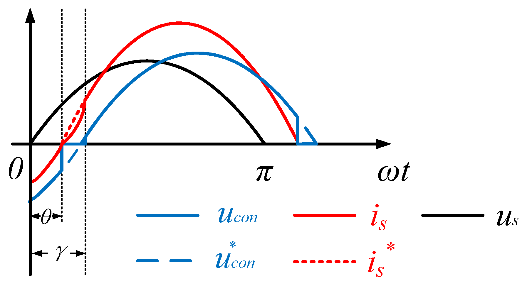
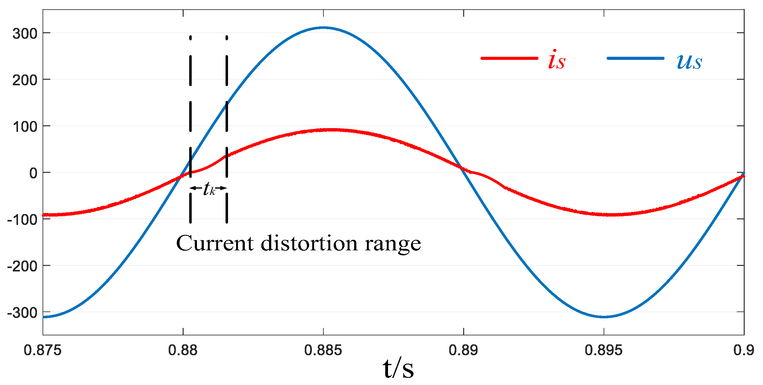
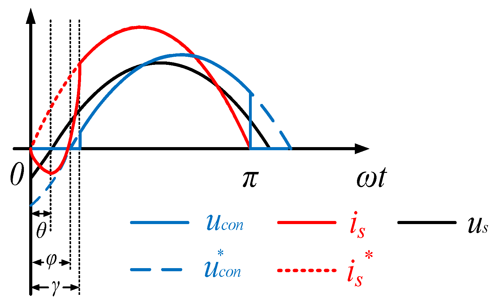
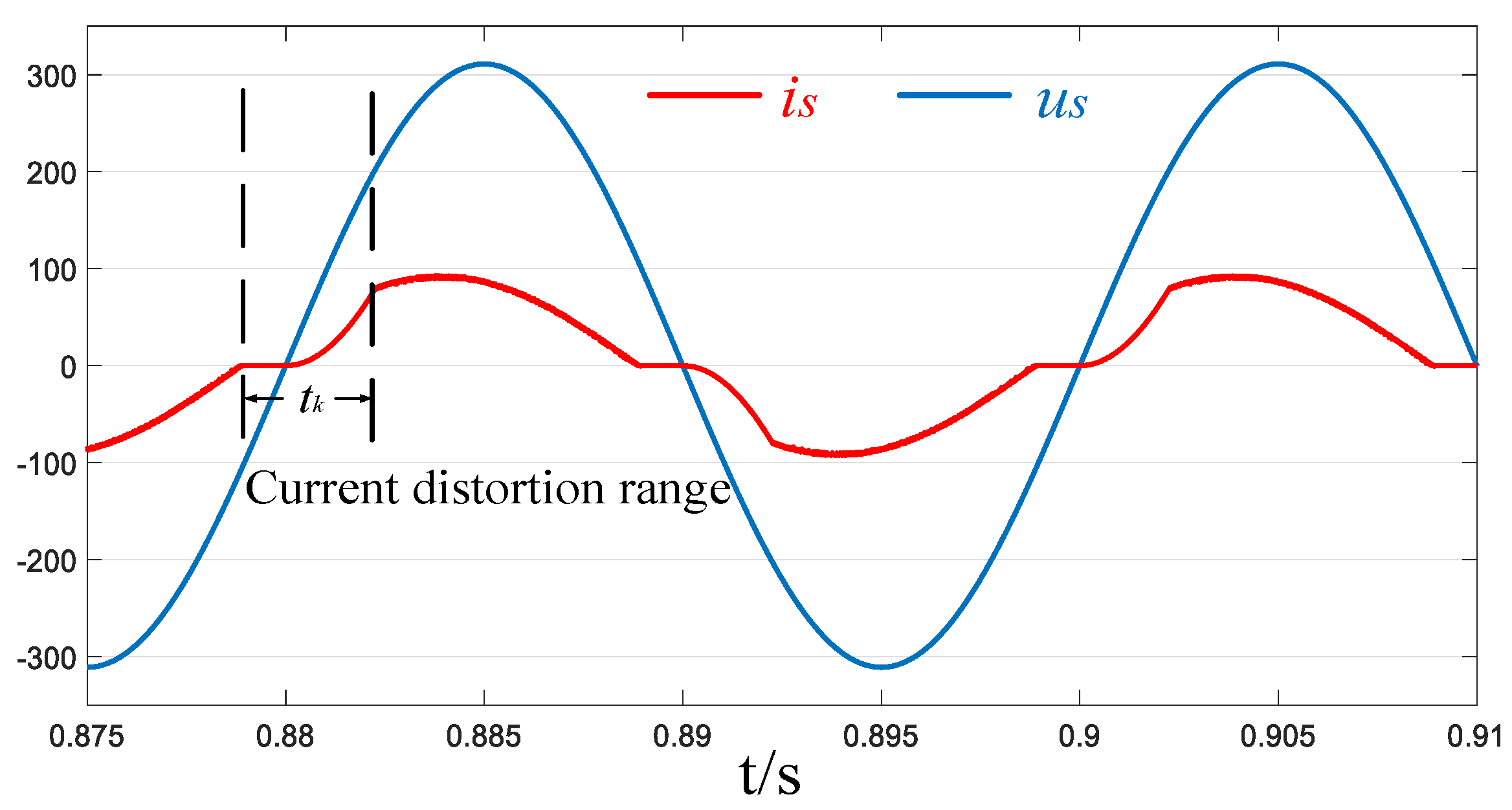
3.1. Theory for Input Current Zero-Crossing Distortion

Due to the unidirectional power flow for the bridgeless rectifier, whenever the polarities of the current and voltage on the AC side of the rectifier switch, an input current distortion appears. The steady state AC side phasor diagram is shown in Figure 5, where U c o n * and I s * are the reference voltage and reference current on the AC side of the rectifier, respectively. When the rectifier is operating under a unity power factor, the input current I s is in phase with the source voltage U s , and the voltage across the input inductor U L is orthogonal to I s . According to the triangle law of vector addition, U c o n lags I s by θ, as shown in Figure 5. This lagging angle θ indicates that, during the period of θ after the current crosses zero, the input current i s and the AC-side voltage u c o n are required to have opposite polarities. However, due to the unidirectional power flow, the AC-side voltage and current of the bridgeless rectifier must have the same polarity. Hence, during this period, AC-side voltage u c o n can only be kept at zero, which makes the input current uncontrollable [18,19]. Note that the heavier the loads, the more serious the input current zero-crossing distortion.
From the above analysis, the current zero-crossing distortion is generated under leading, lagging, and unity power factor. As the leading or lagging angle increases, the current distortion becomes more severe. Notably, the distortion of the input current under a leading power factor is more severe than the distortion of the input current under a lagging power factor. Section 3.2, Section 3.3 and Section 3.4 discuss the input current distortion under unity power factor, leading power factor, and lagging power factor in detail, respectively, and describe the input current distortion by piecewise function in each part.

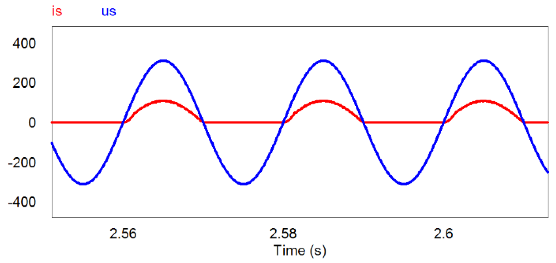
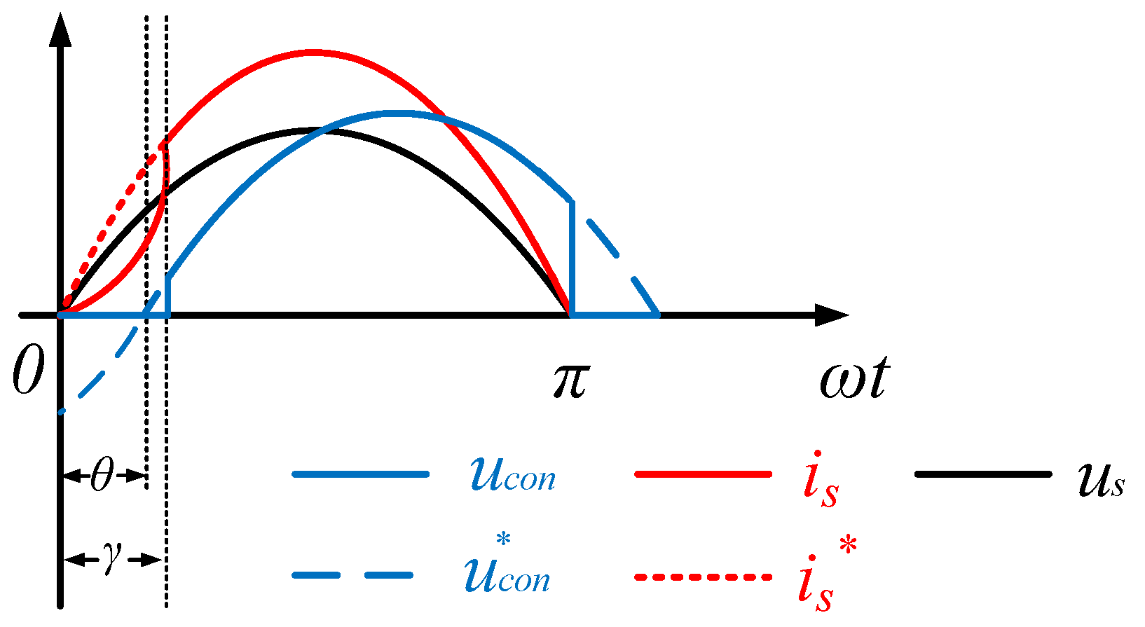
3.2. Distortion Characteristics of Input Current under Unity Power Factor

Figure 6 displays an AC-side phasor diagram under a unity power factor. Considering the symmetry, only the half-cycle waveform is analyzed.
The grid voltage us, reference input current i*s, and reference voltage on the AC side of the rectifier u*con under a unity power factor can be expressed as follows:
u s = U s m sin ω t
i s * = I s m sin ω t
u c o n * = U c o n m sin ( ω t θ )
If i s * > 0 and u c o n * <   0 within the range of 0–θ, the u c o n cannot follow u c o n * . In this period, u c o n is clamped to zero, and u s = u L . Accordingly, i s is expressed as:
i s ( t ) = U s m L 0 t sin ( ω τ ) d τ = U s m ω L ( 1 cos ( ω t ) )
When ωt = θ, the polarity of u c o n * is reversed from negative to positive, and u c o n has the ability to follow u c o n * , theoretically. However, as i s * > i s , in order to make is follow i s * , u c o n is still maintained at zero until i s = i s * over a period of ωt > θ. Let i s = i s * when ωt = γ, as:
U s m ω L ( 1 cos ( ω t k ) ) = I s m sin ( ω t k )
γ = 2 arctan ( ω L I s m U s m )
Therefore, the piecewise function of the input current in a power frequency cycle is expressed as
i s ( t ) = { U s m ω L ( 1 cos ( ω t ) ) , 0 < ω t γ I s m sin ω t , γ < ω t π U s m ω L ( 1 cos ( ω t ) ) , π < ω t π + γ I s m sin ω t , π + γ < ω t 2 π
The RMS value of fundamental component of input current is
I s m 1 R M S = a 2 + b 2 2
where:
a = 2 U s m π ω L ( sin γ 1 2 γ 1 4 sin 2 γ ) + I s m 2 π ( cos 2 γ 1 )
b = 2 U s m π ω L ( cos γ + 1 4 cos 2 γ + 3 4 ) + I s m π ( 1 2 sin 2 γ γ + π )
The Root Mean Square (RMS) value of input current is:
I s m R M S = ω 2 π 0 2 π ω i s 2 ( t ) d t = ( U s m 2 4 π ω 2 L 2 + I s m 2 4 π ) sin 2 γ 2 U s m 2 π ω 2 L 2 sin γ + ( 3 U s m 2 2 π ω 2 L 2 I s m 2 2 π ) γ + I s m 2 2
where Ism can be obtained based on conservation of power, as:
I s m = 2 U s m U d c 2 R
THD of input current can be deduced as:
T H D = I s m R M S 2 I s m 1 R M S 2 I s m 1 R M S
Note that the above analytical methods can be applied to both driving modes.

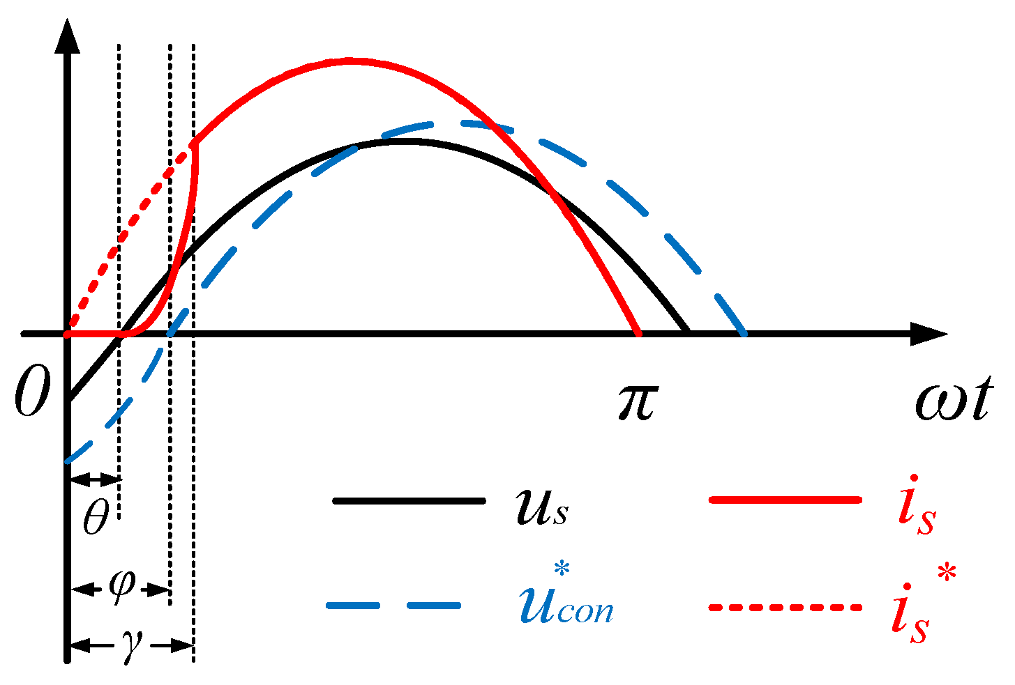
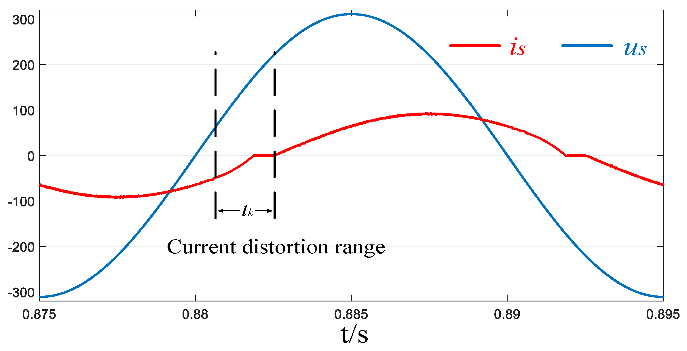
3.3. Distortion Characteristics of Input Current under Leading Power Factor

Figure 7 shows the AC-side fundamental waveform of a system with a synchronous drive. When ωt = 0, the polarity of i s * is reversed from negative to positive, u c o n is zero, and the polarity of u s is negative, which leads to the negative increase in u s . The rate of increase of | i s * | is larger than that of | i s | in the heavy load. In order to make | i s | follow | i s * | , u c o n is clamped to zero until i s = i s * when ωt = γ. The amplitude of i s * is smaller in the underloading. i s = i s * can be achieved within a certain period after reversing the polarity of is. When us approaches 0, the growth rate of | i s | decreases. The change rate of is is 0 when ωt = θ, | i s | < | i s * | . Then us reverses its polarity. To make | i s | follow | i s * | , u c o n is clamped to zero until i s = i s * . The current distortion process will end at this point.
Figure 8 shows the AC-side fundamental waveforms with complementary drive. When ωt = 0, the polarity of i s * is reversed from negative to positive, u c o n is zero, and the polarity of u s is negative, which leads to the negative increase in u s . At this moment, the polarity of i s is negative. As i s * i s > 0 , the current control loop causes the duty ratio dS1 of S1 to increase and the duty ratio dS2 of S2 to decrease. Based on the negative polarity of u s , | i s | decreases with the decrease in dS2. Once the polarity of i s has reversed its polarity from negative to positive, the polarity of i s reverses to negative again due to u c o n = 0 . This control places i s in a discontinuous state when 0 < ωt < θ. When θ < ωt < γ and u s > 0 , in order to make i s follow i s * , ucon is clamped to zero until i s = i s * when ωt = γ. The current distortion process will end at this point.
The piecewise function expression of the input current is:
i s ( t ) = { 0 , 0 < ω t θ U s m ω L ( 1 cos ( ω t θ ) ) , θ < ω t γ I s m sin ω t , γ < ω t π 0 , π < ω t π + θ U s m ω L ( 1 cos ( ω t θ ) ) , π + θ < ω t π + γ I s m sin ω t , π + γ ω t < 2 π
Let i s = i s * at ωtk = γ. γ can be expressed as:
γ = arctan ( U s m sin θ + ω L I s m U s m cos θ ) + arctan ( ω 2 L 2 I s m 2 + 2 ω L U s m I s m sin θ U s m )
The comparison shows that the current distortion becomes more severe under synchronous driving. Therefore, the complementary drive is a more appropriate choice under a leading power factor.

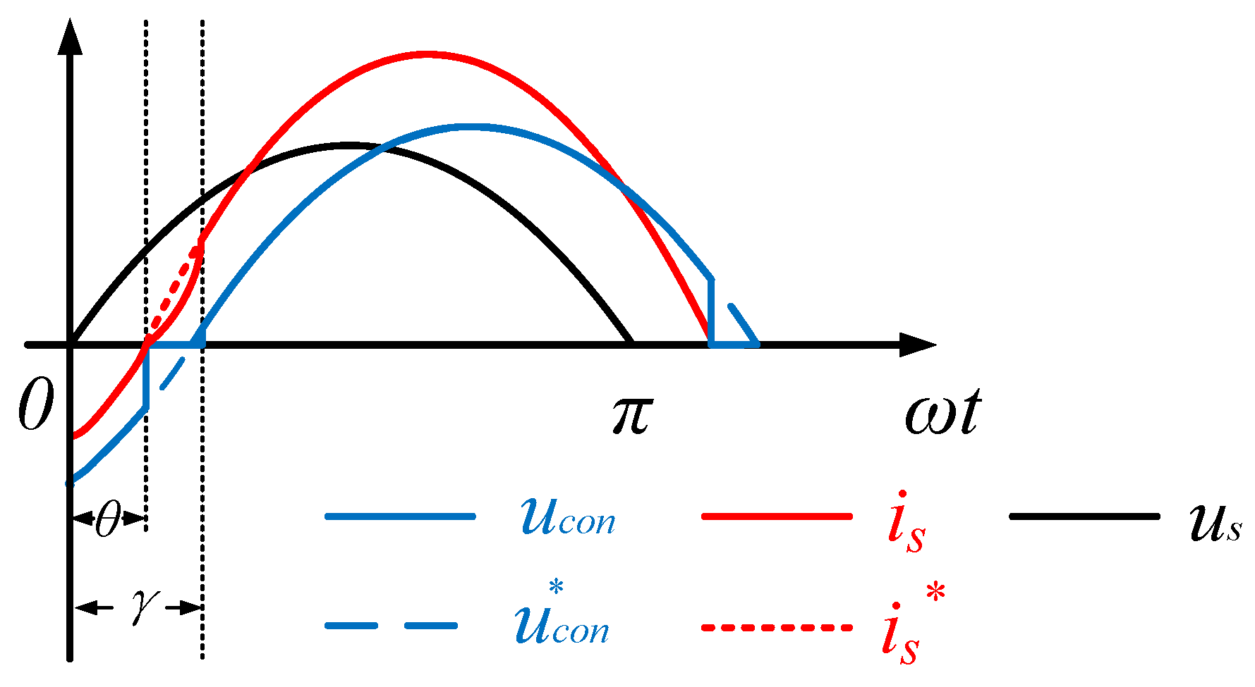
3.4. Distortion Characteristics of Input Current under Lagging Power Factor

When the angle of the lagging power factor is θ under a complementary drive, there are two phase relations between the AC-side voltage and the input current according to the value of |uL| and |ussinθ|. In Figure 9, is goes ahead of ucon. Based on the above analysis, the piecewise function expression of is is:
i s ( t ) = { I s m sin ( ω t θ ) , 0 < ω t θ U s m ω L ( cos θ cos ( ω t ) ) , θ < ω t γ I s m sin ( ω t θ ) , γ < ω t π + θ U s m ω L ( cos θ cos ( ω t ) ) , π + θ < ω t π + γ I s m sin ( ω t θ ) , π + γ < ω t 2 π
Let i s = i s * at ωtk = γ. γ can be expressed as:
γ = arctan ( ω L I s m cos θ U s m ω L I s m sin θ ) + arctan ( ( U s m sin θ ω L I s m ) 2 U s m cos θ )
is lags ucon as shown in Figure 10, and its piecewise function expression is:
i s ( t ) = { I s m sin ( ω t θ ) , 0 < ω t φ I s m sin ( φ θ ) + U s m ω L ( cos φ cos ω t ) , φ < ω t γ 0 , γ < ω t θ I s m sin ( ω t θ ) , θ < ω t π + φ I s m sin ( φ θ ) U s m ω L ( cos φ + cos ω t ) , π + φ < ω t π + γ 0 , π + γ < ω t π + θ I s m sin ( ω t θ ) , π + θ < ω t 2 π
Based on cosine law, the angle φ of ucon that lags us can be deduced:
φ = arccos ( U s m ω L I s m sin θ U s m 2 + ω 2 L 2 I s m 2 2 ω L I s m U s m sin θ )
Let is = 0 when ωtk = γ, yielding:
γ = arccos ( ω L I s m U s m sin ( φ θ ) + cos φ )

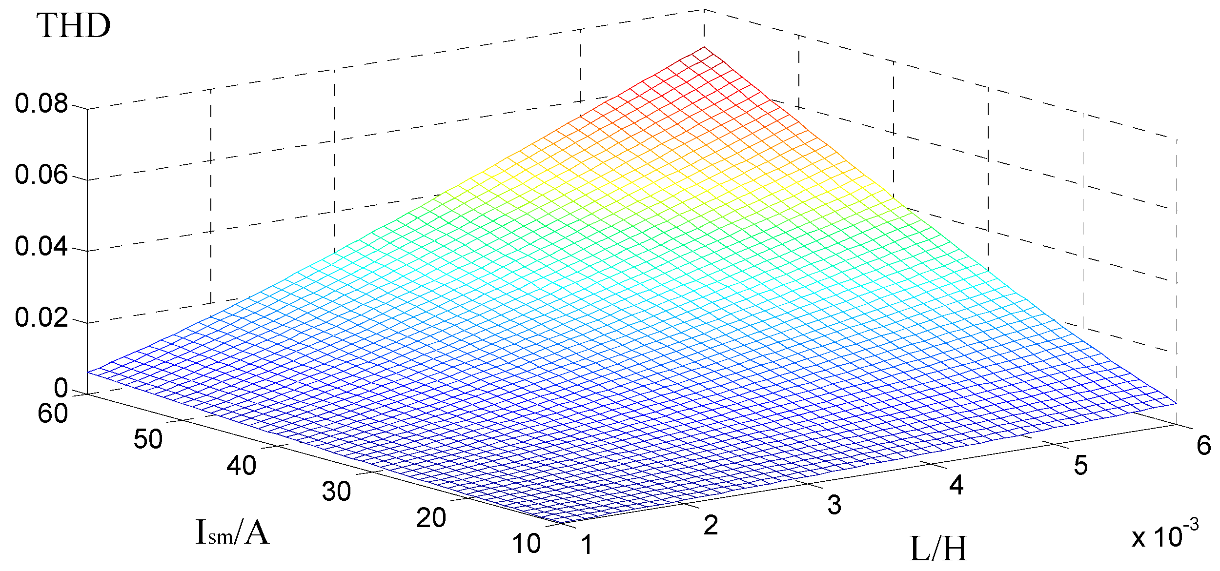
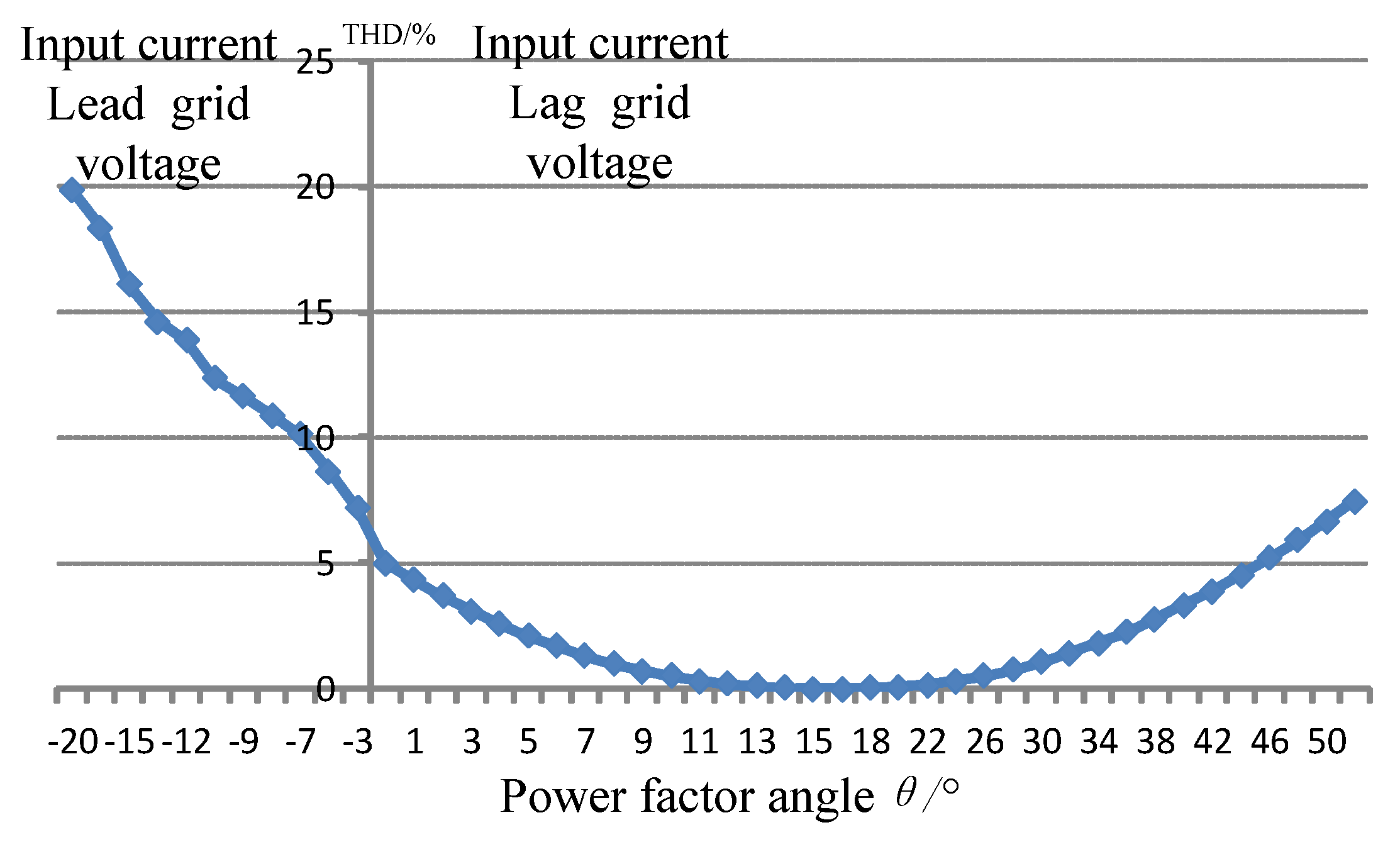
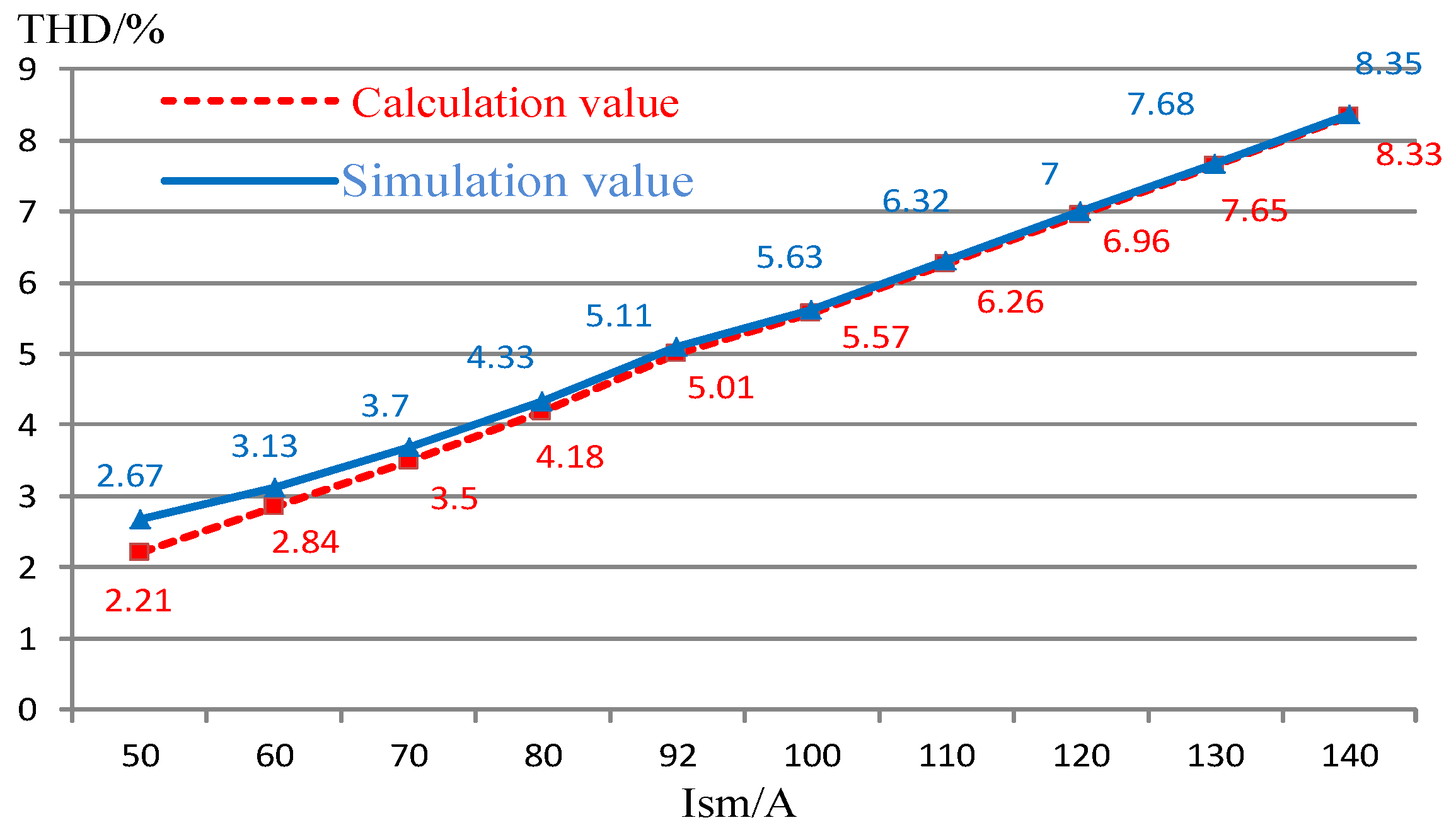
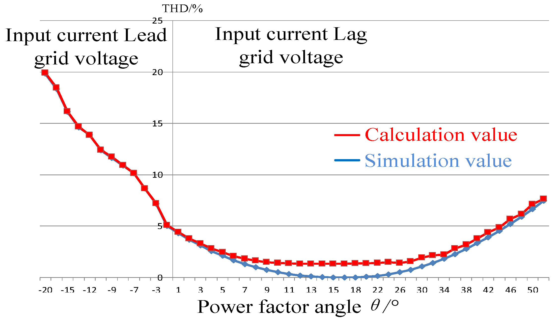
4. Constrain of Input Current on Filter Inductance, Input Current Amplitude, and Power Factor Angel Based on THD

Based on the above analysis, the input current zero-crossing distortion is affected by filter inductance L, input current amplitude Ism, and power factor angle θ. Therefore, the allowable range of THD restricts the value of L, Ism, and θ.
At first, the limitation of THD on L and Ism was investigated. Taking θ = 0° as an example, Figure 11 shows the relation between current THD and L and Ism when Usm = 311 V, f = 50 Hz, and Udc = 400 V. When L was chosen from 1–6 mH, and Ism was changed from 10 to 60 A, the degree of input current distortion was aggravated with the increase in L and Ism, and the maximum THD reached 6.96%. Figure 12 shows the contour line of THD with current and inductance when Usm = 311 V, f = 50 Hz, and Udc = 400 V. The values of L and Ism can be determined based on the allowable range. For example, the shaded area in Figure 12 is the limitation on L and Ism when THD < 1.4%. It is assumed that Ism = 40 A, so 2.5 mH inductance can be selected when the THD of the current requirements are satisfied. In this case, THD was about 1.25%. In practical applications, if the THD of the equipment current is above 5%, the equipment will not be allowed to connect to the grid. Hence, the contour line of current 5% THD should be drawn and the RPC and HCC functionalities of bridgeless rectifiers should be limited in practical applications.
If the value of L and Ism are determined in the design, the range of power factor angle θ can be determined based on the allowable range of THD. This also demonstrates the relation between THD and θ. Under the conditions where Ism = 92 A, Usm = 311 V, and L = 3 mH (θ less than zero refers to input current phase leading grid voltage phase), Figure 13 can be obtained. When the current phase leads the grid voltage phase, THD increases rapidly with the leading angle. When the current lags grid voltage by about 16°, the theorical value of THD is closer to zero because the AC-side voltage and input current are in the same phase position at this moment, and no polarity opposite exists in this period, thus avoiding current zero-crossing distortion. When the current lags grid voltage more than 16°, THD increases with the lagging angle, but the degree is less than that when the current leads the grid voltage. The range of the power factor angle can be determined from Figure 13 to ensure THD falls within the allowable range, which actually determines the reactive compensation capacity of the bridgeless rectifier. In conclusion, the mathematical analysis of the current distortion can be used to select filter inductance, input current amplitude, and power factor angle.

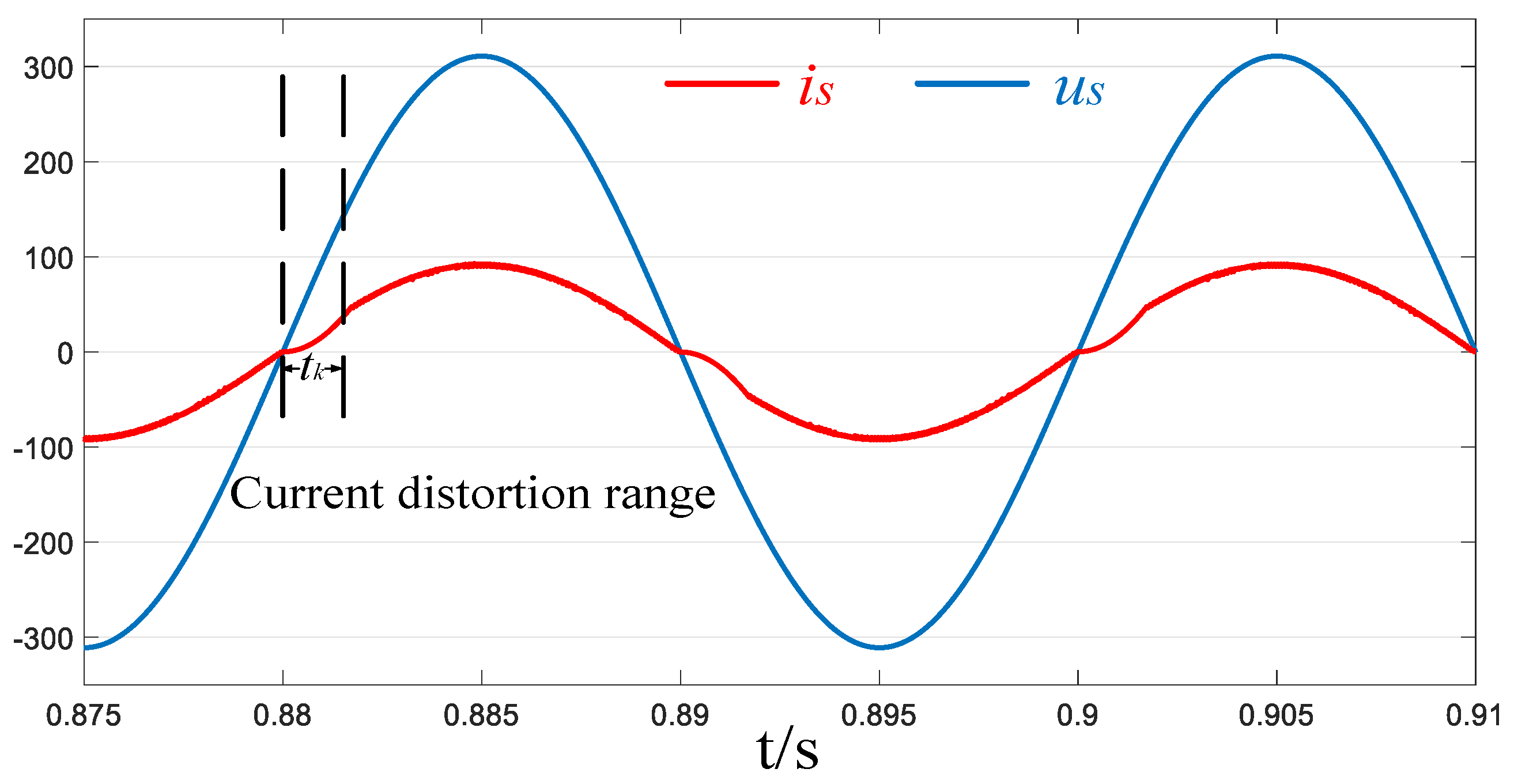
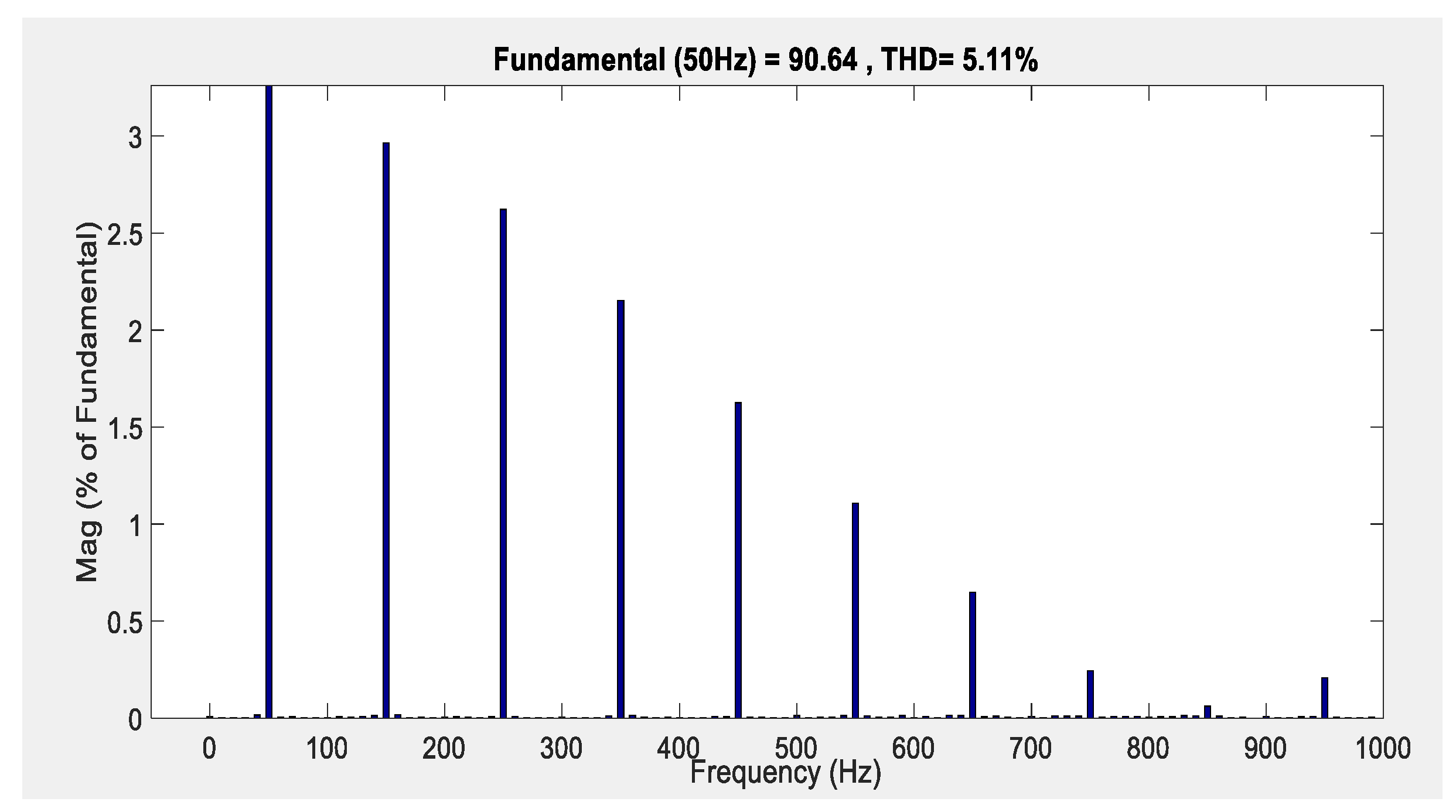
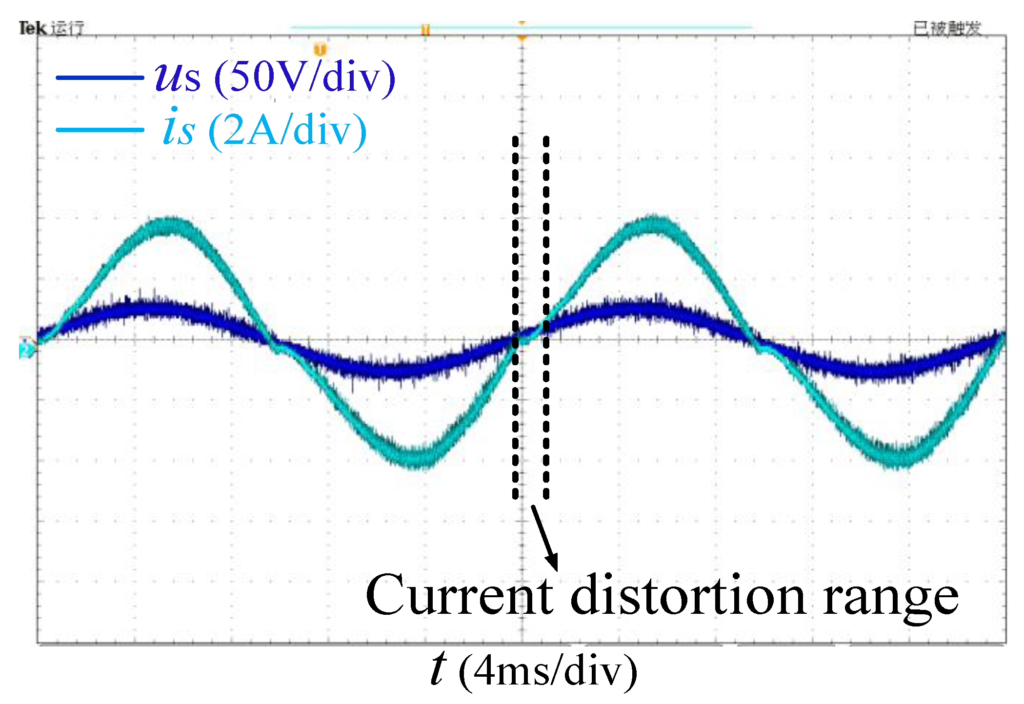
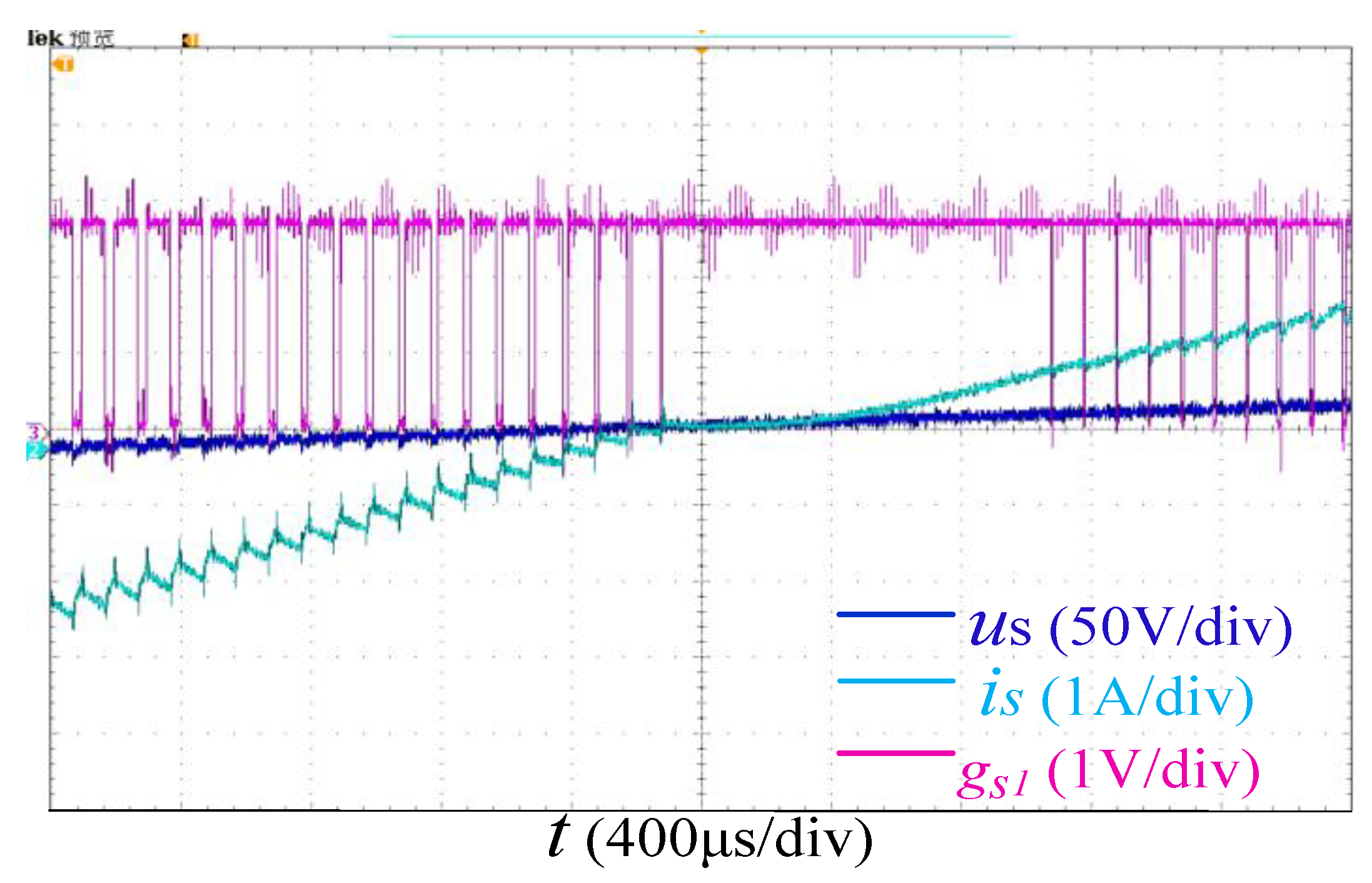
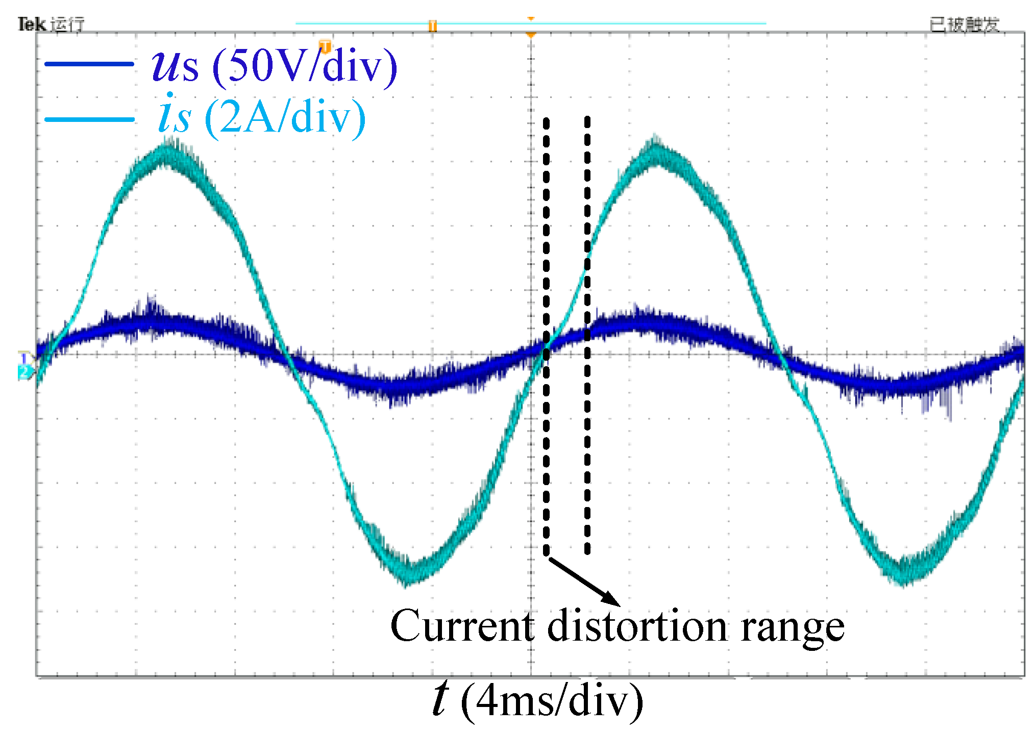
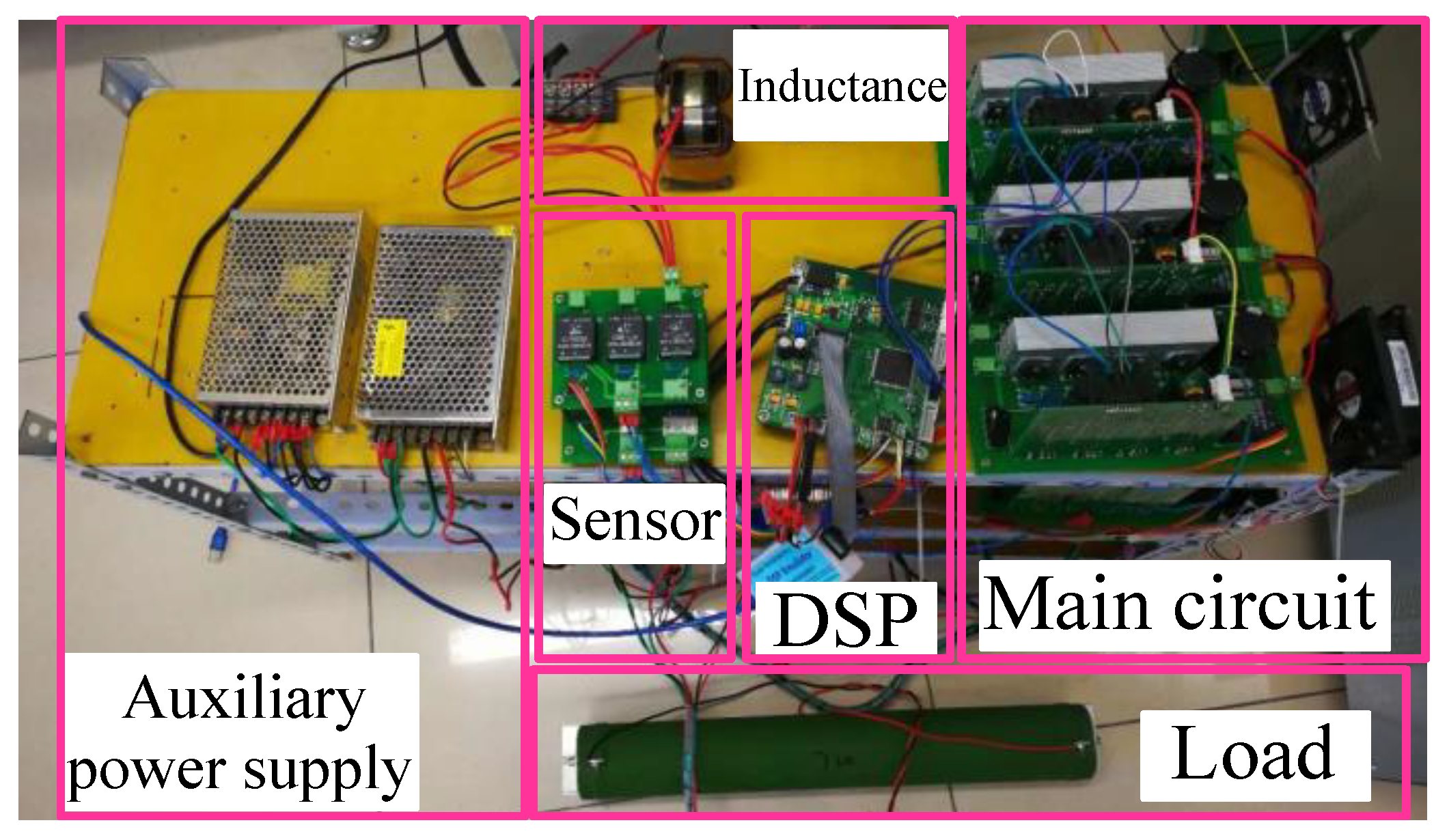
5. Simulation and Experimental Results

A simulation model of a bridgeless rectifier was set up based on MATLAB/Simulink (9.3.0.713579 (R2017b), MathWorks, Natick, MA, USA). The simulation main parameters are shown in Table 2.
In order to reduce the current distortion, the complementary drive was adopted for the simulation. Figure 14 depicts the simulation waveforms of the grid voltage and input current under a unity power factor. Voltage and current are in phase, and the current is obviously distorted at the point. The distortion angle is 0.523 radians. The current THD shown in Figure 15 is 5.11%. The theoretical value of distortion angle is 0.5438 radians, and THD theoretical value was 5.01%. Therefore, the theoretical value is basically the same as the simulation result.
Figure 16 shows the theoretical value of THD and the simulation value of THD under different Ism. They are basically identical through comparison. Figure 17 depicts the simulation waveforms of the grid voltage and input current when the input current led the grid voltage by 20°. UL > |Ussinθ| when the angle that the input current lagged grid voltage was 5°, and the simulation waveforms of grid voltage and input current are shown in Figure 18. UL < |Ussinθ| when the input current lagged the grid voltage by 45°. The simulation waveforms of the grid voltage and input current are shown in Figure 19. The above simulation waveforms basically conform to the theoretical analysis.
Figure 20 shows the relation between theoretical value of THD and simulation value of THD with θ under the conditions of Ism = 92 A, Usm = 311 V, and L = 3 mH. The theoretical value is basically the same as the simulation result. It should be noted that the switching frequency and the higher harmonic of its multiple were ignored when the THD was calculated. However, the smaller the THD, the larger the proportion of higher harmonic in current distortion. Therefore, when THD is closer to zero, its theoretical value is slightly less than the simulation value.
The down-scale prototype of a bridgeless rectifier was set up with TMS320F28335 as a core controller. The parameters of this prototype are provided in Table 3. IXFH46N65X2 46-A 650-V MOSFETs, and IDW15E65D2 30-A 650-V power silicon diodes were employed throughout. Aluminum electrolyte capacitors and input inductor with a Toroidal Ferrite Core and 117 turns of 0.1 × 200 Litzy wire were also adopted in this experiment, on DC side AC side, respectively.
Complementary drive mode as adopted. The downscaled prototype is shown in Figure 21.
Figure 22 shows the waveform of us and is under a unity power factor. The zero-crossing points of is coincided with us, and is distorted based approximately on the cosine law in the period after crossing the zero point. Figure 23 shows the zoomed-in waveforms of driving signals gS1 and is of us and S1. us > 0 during the distortion period of is, whereas S1 remains in conduction in order to make ucon approximate zero. All the above experiment results satisfy the theoretical analysis.
Figure 24 shows the experiment waveforms of us and is under a leading power factor. is stays near zero within a period after crossing zero. us gradually turns to sine waveform after crossing zero, which satisfies the proposed theoretical analysis. Figure 25 and Figure 26 show the experiment waveforms of us and is when the angles is lag us by 8°and 40°, respectively. When the lagging angle is 8°, UL > |Ussinθ|. When it is 40°, UL < |Ussinθ|. These experimental waveforms basically conform to the theoretical analysis and simulation waveforms.

6. Conclusions

In order to more effectively integrate the RPC and HCC capabilities into the bridgeless rectifier, the input current harmonic characteristic of bridgeless rectifier under different power factors in two driving modes is discussed in this paper. Firstly, two driving modes are analyzed. Based on the above analysis, it is concluded that the complementary drive mode is a better choice in terms of reducing the current distortion when bridgeless rectifier operates under non-unity power factor. And then, the mechanism of input current zero-crossing distortion is analyzed. Furthermore, the input current during the distortion is expressed by the piecewise function when a bridgeless rectifier operates under complementary driving mode. Based on the piecewise function, the harmonic analysis is performed. Besides, when bridgeless rectifier operates under non-unity power factor, the above analysis makes the criteria of selecting parameters including the filter inductance, input current amplitude and power factor angle be further improved. Finally, the correctness and effectiveness of proposed theory is verified through the simulation and the experiment.

Author Contributions

J.L. and Y.Z. designed the research; Y.L. finished and collected the experiment and data; C.W. guide the research.

Funding

This research was funded by the National Natural Science Foundation of China grant number 51577187 and The Fundamental Research Funds for the Central Universities grant number 2015QJ11.

Acknowledgments

This work was supported by the National Natural Science Foundation of China under Grant No. 51577187 and The Fundamental Research Funds for the Central Universities (2015QJ11).

Conflicts of Interest

The authors declare no conflict of interest.

References

  1. Hamad, M.S.; Masoud, M.I.; Williams, B.W. Medium-Voltage 12-Pulse Converter: Output Voltage Harmonic Compensation Using a Series APF. IEEE Trans. Ind. Electron. 2014, 61, 43–52. [Google Scholar] [CrossRef]
  2. Sun, X. Study of a Novel Equivalent Model and a Long-Feeder Simulator-Based Active Power Filter in a Closed-Loop Distribution Feeder. IEEE Trans. Ind. Electron. 2016, 63, 2702–2712. [Google Scholar] [CrossRef]
  3. Lam, C.S.; Wang, L.S.; Ho, I.; Wong, M.C. Adaptive Thyristor-Controlled LC-Hybrid Active Power Filter for Reactive Power and Current Harmonics Compensation with Switching Loss Reduction. IEEE Trans. Ind. Electron. 2017, 32, 7577–7590. [Google Scholar] [CrossRef]
  4. Huber, L.; Jang, Y.; Jovanovic, M.M. Performance Evaluation of Bridgeless PFC Boost Rectifiers. IEEE Trans. Power Electron. 2008, 23, 1381–1390. [Google Scholar] [CrossRef]
  5. Liu, L.; Li, H.; Xue, Y.; Liu, W. Reactive Power Compensation and Optimization Strategy for Grid-Interactive Cascaded Photovoltaic Systems. IEEE Trans. Power Electron. 2015, 30, 188–202. [Google Scholar] [CrossRef]
  6. Singh, M.; Khadkikar, V.; Chandra, A.; Varma, R.K. Grid interconnection of renewable energy sources at the distribution level with power quality improvement features. IEEE Trans. Power Deliv. 2011, 26, 307–315. [Google Scholar] [CrossRef]
  7. Kisacikoglu, M.C.; Ozpineci, B.; Tolbert, L.M. EV/PHEV bidirectional charger assessment for V2G reactive power operation. IEEE Trans. Power Electron. 2013, 28, 5717–5727. [Google Scholar] [CrossRef]
  8. Wang, C.; Zhuang, Y.; Jiao, J.; Zhang, H.; Wang, C.; Cheng, H. Topologies and Control Strategies of Cascaded Bridgeless Multilevel Rectifiers. IEEE J. Emerg. Sel. Top. Power Electron. 2017, 5, 432–444. [Google Scholar] [CrossRef]
  9. Ma, H.; Lai, J.; Zheng, C.; Sun, P. A High-Efficiency Quasi-Single-Stage Bridgeless Electrolytic Capacitor-Free High-Power AC–DC Driver for Supplying Multiple LED Strings in Parallel. IEEE Trans. Power Electron. 2016, 8, 5825–5836. [Google Scholar] [CrossRef]
  10. Park, S.M.; Park, S.Y. Versatile unidirectional AC-DC converter with harmonic current and reactive power compensation for smart grid applications. In Proceedings of the 2014 IEEE Applied Power Electronics Conference and Exposition—APEC 2014, Fort Worth, TX, USA, 16–20 March 2014; pp. 2163–2170. [Google Scholar]
  11. Fardoun, A.; Ismail, E.; Al-Saffar, M.; Sabzali, A. A Bridgeless Resonant Pseudoboost PFC Rectifier. IEEE Trans. Power Electron. 2014, 11, 5949–5960. [Google Scholar] [CrossRef]
  12. Zhao, B.; Abramovitz, A.; Smedley, K. Family of Bridgeless Buck-Boost PFC Rectifiers. IEEE Trans. Power Electron. 2015, 30, 6524–6527. [Google Scholar] [CrossRef]
  13. Lin, X.; Wang, F. New Bridgeless Buck PFC Converter with Improved Input Current and Power Factor. IEEE Trans. Ind. Electron. 2018, 10, 7730–7740. [Google Scholar] [CrossRef]
  14. Liu, Y.; Sun, Y.; Su, M. A Control Method for Bridgeless Cuk/Sepic PFC Rectifier to Achieve Power Decoupling. IEEE Trans. Ind. Electron. 2017, 9, 7272–7276. [Google Scholar] [CrossRef]
  15. Jian, J.; Cong, W. The research of new cascade bridgeless multi-level rectifier. In Proceedings of the 2014 International Power Electronics and Application Conference and Exposition, Shanghai, China, 5–8 December 2014; pp. 1513–1518. [Google Scholar]
  16. Chang, W.; Cong, W.; Wang, K.; Hong, C.; Liang, Y. New control algorithm of bridgeless PFC. Adv. Technol. Electr. Eng. Energy 2015, 34, 18–23. [Google Scholar]
  17. Park, S.M.; Park, S.Y. Versatile control of unidirectional AC–DC boost converters for power quality mitigation. IEEE Trans. Power Electron. 2015, 30, 4738–4749. [Google Scholar] [CrossRef]
  18. Kotsopoulos, A.; Heskes, P.J.M.; Jansen, M.J. Zero-crossing distortion in grid-connected PV inverters. IEEE Trans. Ind. Electron. 2005, 52, 558–565. [Google Scholar] [CrossRef]
  19. Wu, F.; Sun, B.; Zhao, K.; Sun, L. Analysis and Solution of Current Zero-Crossing Distortion with Unipolar Hysteresis Current Control in Grid-Connected Inverter. IEEE Trans. Ind. Electron. 2013, 60, 4450–4457. [Google Scholar] [CrossRef]
Figure 1. Main topology of the bridgeless rectifier and its four operation modes: (a) Main topology of the bridgeless rectifier; (b) Mode I; (c) Mode II; (d) Mode III; (e) Mode IV.
Energies 11 02447 g001aEnergies 11 02447 g001b
Figure 2. Block diagram of the complementary drive.
Energies 11 02447 g002
Figure 3. Block diagram for a synchronous drive.
Energies 11 02447 g003
Figure 4. Simulation current waveform on the alternating current (AC) side based on a synchronous drive without an absolute value module.
Energies 11 02447 g004
Figure 5. Phasor diagram on the AC side under unity power factor.
Energies 11 02447 g005
Figure 6. Expected waveforms and actual waveforms of the AC-side fundamental voltage and current of bridgeless rectifier under a unity power factor.
Energies 11 02447 g006
Figure 7. Expected waveforms and actual waveforms of the AC-side fundamental voltage and current with synchronous drive under a leading power factor.
Energies 11 02447 g007
Figure 8. Expected waveforms and actual waveforms of AC side fundamental voltage and current with complementary drive under leading power factor.
Energies 11 02447 g008
Figure 9. Expected waveforms and actual waveforms of AC-side fundamental voltage and current under a lagging power factor (UL > |Ussinθ|).
Energies 11 02447 g009
Figure 10. Expected waveforms and actual waveforms of AC side fundamental voltage and current under lagging power factor (UL < |Ussinθ|).
Energies 11 02447 g010
Figure 11. Three-dimensional (3D) diagram of current total harmonic distortion (THD) under a unity power factor.
Energies 11 02447 g011
Figure 12. Contour line of current THD under a unity power factor.
Energies 11 02447 g012
Figure 13. Relations between THD and power factor angle θ.
Energies 11 02447 g013
Figure 14. Simulation waveforms of grid voltage and input current under unity power factor.
Energies 11 02447 g014
Figure 15. THD analysis of input current under unity power factor.
Energies 11 02447 g015
Figure 16. Theoretical and simulation THD under a unity power factor.
Energies 11 02447 g016
Figure 17. Simulation waveforms of grid voltage and input current under leading power factor.
Energies 11 02447 g017
Figure 18. Simulation waveforms of grid voltage and input current when is lags us by 5°.
Energies 11 02447 g018
Figure 19. Simulation waveforms of grid voltage and input current when is lags us by 45°.
Energies 11 02447 g019
Figure 20. Relationship between theoretical THD and simulation THD with power factor angle θ.
Energies 11 02447 g020
Figure 21. Down-scale experimental prototype.
Energies 11 02447 g021
Figure 22. Experiment waveforms of grid voltage and input current under unity power factor.
Energies 11 02447 g022
Figure 23. Zoomed-in experiment waveforms of grid voltage and input current under unity power factor.
Energies 11 02447 g023
Figure 24. Experiment waveforms of grid voltage and input current under leading power factor.
Energies 11 02447 g024
Figure 25. Experiment waveforms of grid voltage and input current when is lags us by 8°.
Energies 11 02447 g025
Figure 26. Experiment waveforms of grid voltage and input current when is lags us by 40°.
Energies 11 02447 g026
Table 1. Four operation modes of bridgeless rectifiers.
Mode IMode IIMode IIIMode IV
is > 0is < 0
ucon = Udcucon = 0ucon = −Udcucon = 0
D1, DS2 conductivityS1, DS2 conductivityD2, DS1 conductivityS2, DS1 conductivity
Table 2. Main parameters of the simulation.
ParametersValue
Input voltage (RMS)220 V
Source voltage frequency50 Hz
Input current (RMS)65 A
Input inductance3 mH
Switching frequency5 kHz
Load side capacitance4700 uF
DC-link resistance0.09 Ω
DC-link voltage400 V
Table 3. The main parameters of the experiments.
ParameterValue
Input voltage (RMS)24 V
Source voltage frequency50 Hz
Input current (RMS)1.37 A
Input inductance5 mH
Switching frequency5 kHz
Load side capacitance2200 uF
DC-link resistance50 Ω
DC-link voltage40 V

