Design of Multilayer Ring Emitter Based on Metamaterial for Thermophotovoltaic Applications


Abstract
1. Introduction
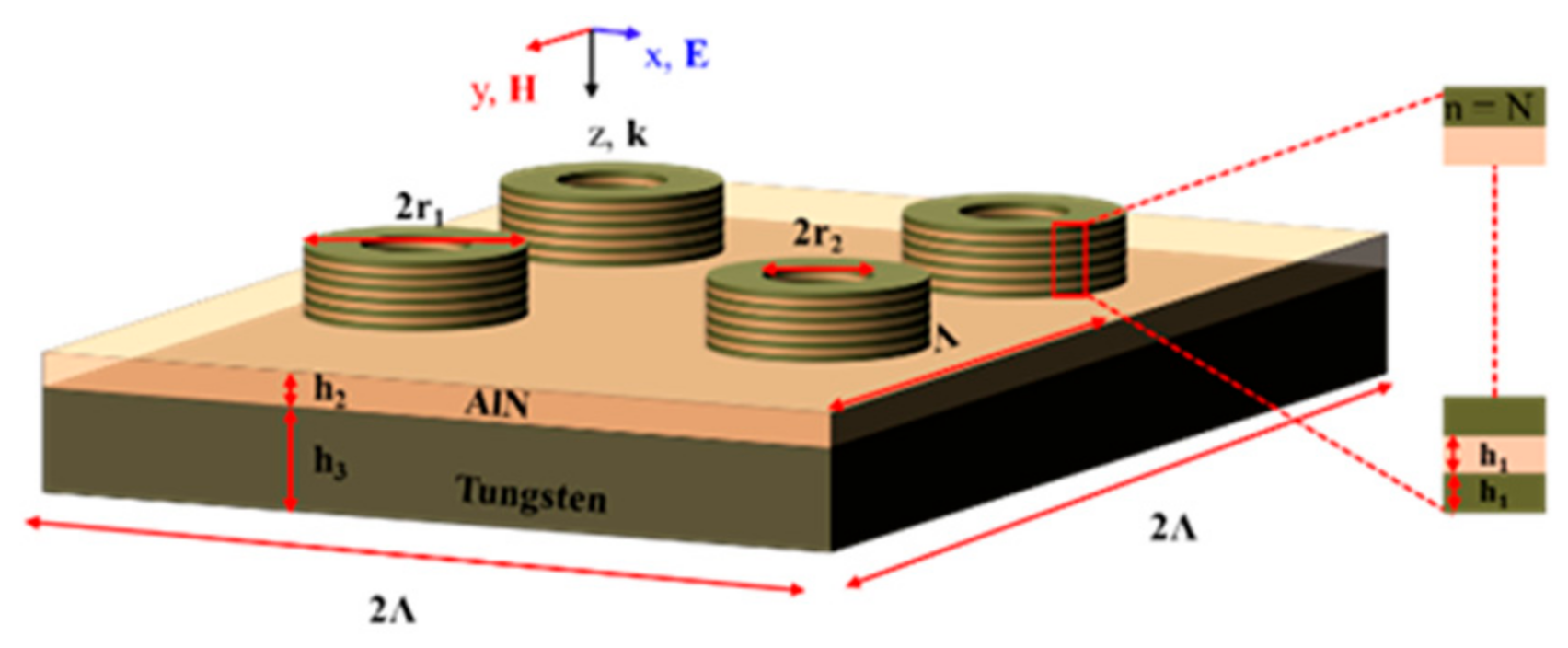
2. Research Methods
3. Result and Discussion
3.1. Effect of Number of Layers (n) and Outer Radius (r1)
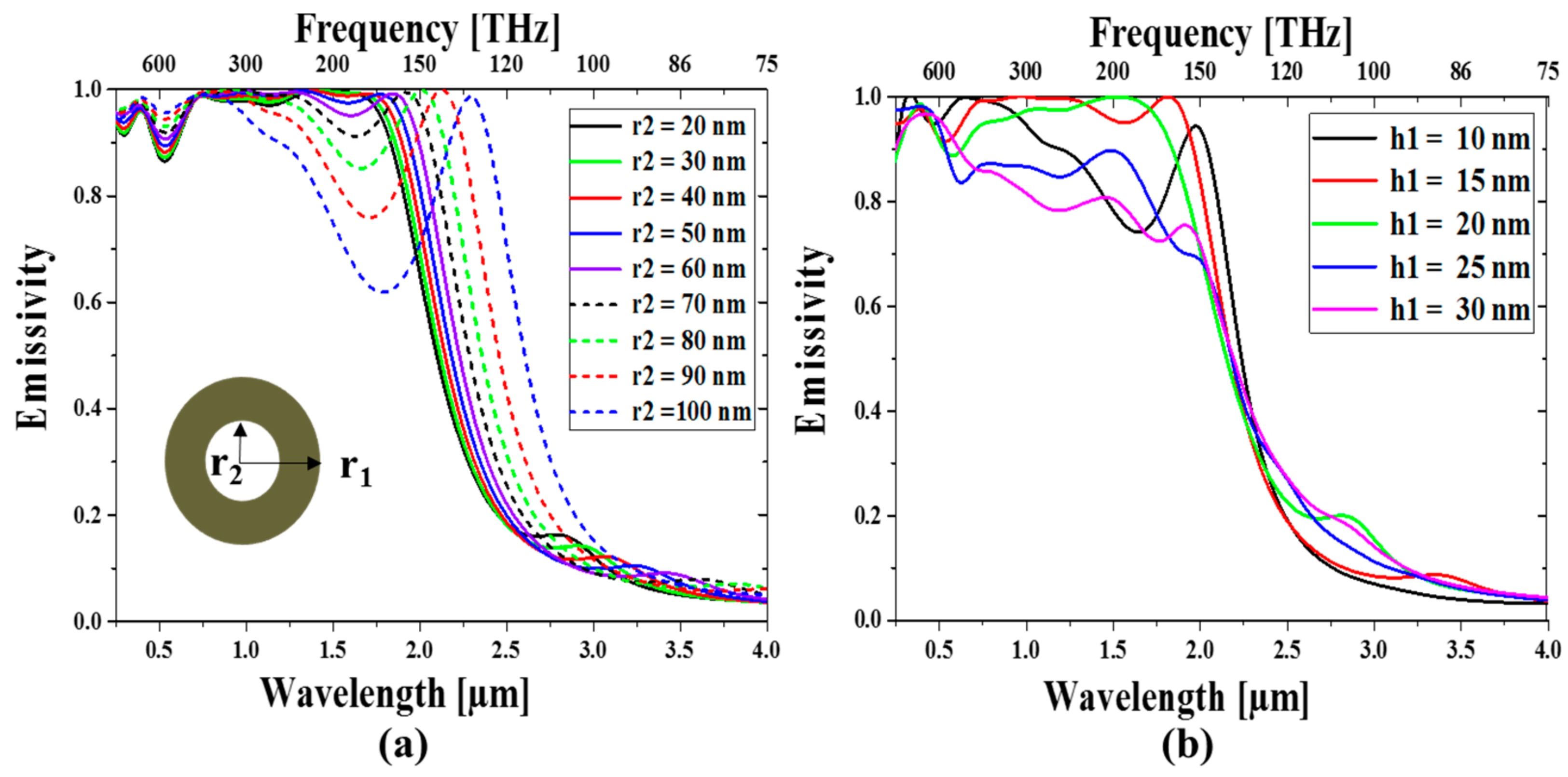
3.2. Effect of Inner Radius (r2) and Thickness of Nano-Ring (h1)
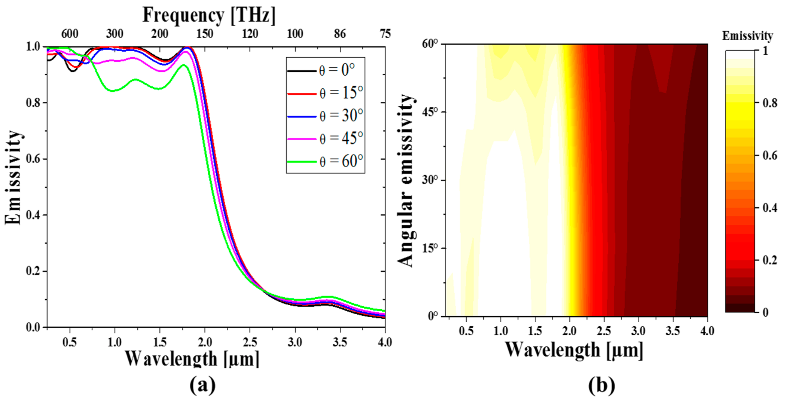
3.3. Angular Emissivity
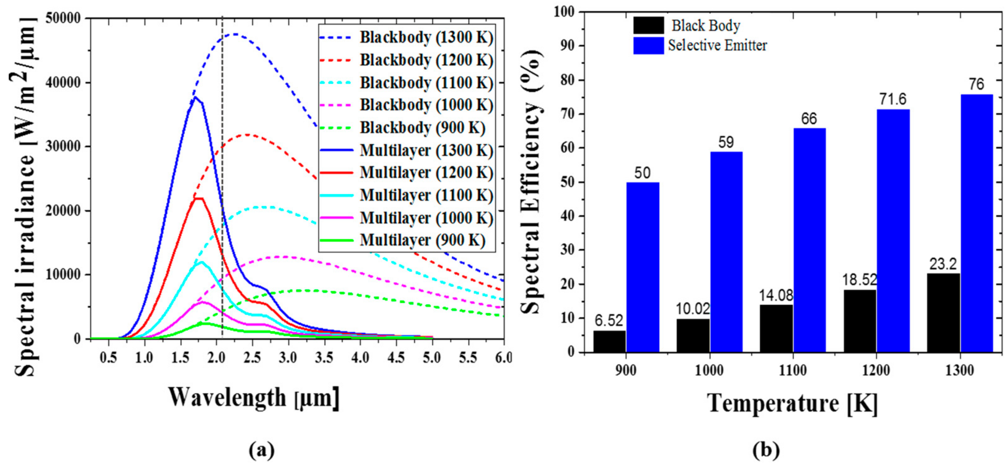
3.4. Performance of TPV
4. Conclusions
Author Contributions
Acknowledgments
Conflicts of Interest
References
- Jin, S.; Lim, M.; Lee, S.S.; Lee, B.J. Hyperbolic metamaterial-based near-field thermophotovoltaic system for hundreds of nanometer vacuum gap. Opt. Express 2016, 24, A635–A649. [Google Scholar] [CrossRef] [PubMed]
- Woolf, D.N.; Kadlec, E.A.; Bethke, D.; Grine, A.D.; Nogan, J.J.; Cederberg, J.G.; Hensley, J.M. High-efficiency thermophotovoltaic energy conversion enabled by a metamaterial selective emitter. Optica 2018, 5, 213–218. [Google Scholar] [CrossRef]
- Ghanekar, A.; Lin, L.; Zheng, Y. Novel and efficient Mie-metamaterial thermal emitter for thermophotovoltaic systems. Opt. Express 2016, 24, A868–A877. [Google Scholar] [CrossRef] [PubMed]
- Tong, J.K.; Hsu, W.-C.H.; Huang, Y.; Boriskina, S.V.; Chen, G. Thin-film 'Thermal Well' Emitters and Absorbers for High-Efficiency Thermophotovoltaics. Sci. Rep. 2015, 5. [Google Scholar] [CrossRef] [PubMed]
- Nguyen-Huu, N.; Pistora, J.; Cada, M. Wavelength-selective emitters with pyramid nanogratings enhanced by multiple resonance modes. Nanotechnology 2016, 27. [Google Scholar] [CrossRef] [PubMed]
- Song, J.; Wu, H.; Cheng, Q.; Zhao, J. 1D trilayer films grating with W/SiO2/W structure as a wavelength-selective emitter for thermophotovoltaic applications. J. Quant. Spectrosc. Radiat. Transf. 2015, 158, 136–144. [Google Scholar] [CrossRef]
- Wang, L.P.; Zhang, Z.M. Wavelength-selective and diffuse emitter enhanced by magnetic polaritons for thermophotovoltaics. Appl. Phys. Lett. 2012, 100. [Google Scholar] [CrossRef]
- Song, J.; Si, M.; Cheng, Q.; Luo, Z. Two-dimensional trilayer grating with a metal/insulator/metal structure as a thermophotovoltaic emitter. Appl. Opt. 2016, 55, 1284–1290. [Google Scholar] [CrossRef] [PubMed]
- Lin, S.Y.; Moreno, J.; Fleming, J.G. Three-dimensional photonic-crystal emitter for thermal photovoltaic power generation. Appl. Phys. Lett. 2003, 83, 380–382. [Google Scholar] [CrossRef]
- Fleming, J.G. Addendum “Three-dimensional photonic-crystal emitter for thermal photovoltaic power generation” (vol 83, pg 380, 2003). Appl. Phys. Lett. 2005, 86, 380. [Google Scholar] [CrossRef]
- Trupke, T.; Wurfel, P.; Green, M.A. Comment on “Three-dimensional photonic-crystal emitter for thermal photovoltaic power generation” [Appl. Phys. Lett., 83, 380 (2003)]. Appl. Phys. Lett. 2004, 84, 1997–1998. [Google Scholar] [CrossRef]
- Hedayati, M.K.; Faupel, F.; Elbahri, M. Review of Plasmonic Nanocomposite Metamaterial Absorber. Materials 2014, 7, 1221–1248. [Google Scholar] [CrossRef] [PubMed]
- Cui, Y.; He, Y.; Jin, Y.; Ding, F.; Yang, L.; Ye, Y.; Zhong, S.; Lin, Y.; He, S. Plasmonic and metamaterial structures as electromagnetic absorbers. Laser Photonics Rev. 2014, 8, 495–520. [Google Scholar] [CrossRef]
- Yan, M.; Dai, J.; Qiu, M. Lithography-free broadband visible light absorber based on a mono-layer of gold nanoparticles. J. Opt. 2014, 16. [Google Scholar] [CrossRef]
- Shemelya, C.; Meo, D.D.; Latham, N.P.; Wu, X.; Bingham, C.; Padilla, W.; Vandervelde, T.E. Stable high temperature metamaterial emitters for thermophotovoltaic applications. Appl. Phys. Lett. 2014, 104. [Google Scholar] [CrossRef]
- Zhao, B.; Wanga, L.; Shuai, Y.; Zhang, Z.M. Thermophotovoltaic emitters based on a two-dimensional grating/thin-film nanostructure. Int. J. Heat Mass Transf. 2013, 67, 637–645. [Google Scholar] [CrossRef]
- Cao, T.; Wang, S.; Wei, C.W. Simulation of tunable metamaterial perfect absorber by modulating Bi2Se3 dielectric function. Mater. Express 2016, 6, 45–52. [Google Scholar] [CrossRef]
- Wang, H.; Chang, J.-Y.; Yang, Y.; Wang, L. Performance analysis of solar thermophotovoltaic conversion enhanced by selective metamaterial absorbers and emitters. Int. J. Heat Mass Transf. 2016, 98, 788–798. [Google Scholar] [CrossRef]
- Liu, X.L.; Tyler, T.; Starr, T.; Starr, A.F.; Jokerst, N.M.; Padilla, W.J. Taming the Blackbody with Infrared Metamaterials as Selective Thermal Emitters. Phys. Rev. Lett. 2011, 107. [Google Scholar] [CrossRef] [PubMed]
- Woolf, D.; Hensley, J.; Cederberg, J.G.; Bethke, D.T.; Grine, A.D.; Shaner, E.A. Heterogeneous metasurface for high temperature selective emission. Appl. Phys. Lett. 2014, 105. [Google Scholar] [CrossRef]
- Wang, H.; Chen, Q.; Wen, L.; Song, S.; Hu, X.; Xu, G. Titanium-nitride-based integrated plasmonic absorber/emitter for solar thermophotovoltaic application. Photonics Res. 2015, 3, 329–334. [Google Scholar] [CrossRef]
- Gu, W.; Tang, G.; Tao, W. High efficiency thermophotovoltaic emitter by metamaterial-based nano-pyramid array. Opt. Express 2015, 23, 30681–30694. [Google Scholar] [CrossRef] [PubMed]
- Rephaeli, E.; Fan, S.H. Absorber and emitter for solar thermophotovoltaic systems to achieve efficiency exceeding the Shockley-Queisser limit. Opt. Express 2009, 17, 15145–15159. [Google Scholar] [CrossRef] [PubMed]
- Ding, F.; Cui, Y.; Ge, X.; Jin, Y.; He, S. Ultra-broadband microwave metamaterial absorber. Appl. Phys. Lett. 2012, 100. [Google Scholar] [CrossRef]
- Wang, H.; Sivan, V.P.; Mitchell, A.; Rosengarten, G.; Phelan, P.; Wang, L. Highly efficient selective metamaterial absorber for high-temperature solar thermal energy harvesting. Sol. Energy Mater. Sol. Cells 2015, 137, 235–242. [Google Scholar] [CrossRef]
- Molesky, S.; Dewalt, C.J.; Jacob, Z. High temperature epsilon-near-zero and epsilon-near-pole metamaterial emitters for thermophotovoltaics. Opt. Express 2013, 21, A96–A110. [Google Scholar] [CrossRef] [PubMed]
- Deng, H.; Wang, T.; Gao, J.; Yang, X. Metamaterial thermal emitters based on nanowire cavities for high-efficiency thermophotovoltaics. J. Opt. 2014, 16. [Google Scholar] [CrossRef]
- Yun, D.; Min, X.Y. Perfect solar absorber based on nanocone structured surface for high-efficiency solar thermoelectric generators. Sci. China-Technol. Sci. 2015, 58, 19–28. [Google Scholar]
- Wen, D.; Yang, H.; Ye, Q.; Li, M.; Guo, L.; Zhang, J. Broadband metamaterial absorber based on a multi-layer structure. Phys. Scr. 2013, 88. [Google Scholar] [CrossRef]
- Adachi, S. Aluminum Nitride (AIN). In Optical Constants of Crystalline and Amorphous Semiconductors; Springer: New York, NY, USA, 1999; pp. 143–151. [Google Scholar]
- Wu, C.; Neuner, B., III; John, J.; Milder, A.; Zollars, B.; Savoy, S.; Shvets, G. Metamaterial-based integrated plasmonic absorber/emitter for solar thermo-photovoltaic systems. J. Opt. 2012, 14, 024005. [Google Scholar] [CrossRef]
- Rakic’, A.D.; Djurisic, A.B.; Elazar, J.M.; Majewski, M.L. Optical properties of metallic films for vertical-cavity optoelectronic devices. Appl. Opt. 1998, 37, 5271–5283. [Google Scholar] [CrossRef]
- Pastrnak, J.; Roskovcova, L. Refraction index measurements on AlN single crystals. Phys. Status Solidi B-Basic Solid State 1966, 14. [Google Scholar] [CrossRef]
- Hwanseong, L.; Taehwan, K.; Fekadu, T.M.; Cho, H.H. Enhancing radiative cooling performance using metal-dielectric-metal metamaterials. J. Mech. Sci. Technol. 2017, 31, 5107–5112. [Google Scholar]
- Mitrofanov, O.; Dominec, F.; Kužel, P.; Reno, J.L.; Brener, I.; Chung, U.-C.; Elissalde, C.; Maglione, M.; Mounaix, P. Near-field probing of Mie resonances in single TiO2 microspheres at terahertz frequencies. Opt. Express 2014, 22, 23034–23042. [Google Scholar] [CrossRef] [PubMed]
- Wang, H.; Wang, L. Perfect selective metamaterial solar absorbers. Opt. express 2013, 21, A1078–A1093. [Google Scholar] [CrossRef] [PubMed]
- Ferrari, C.; Melino, F.; Pinelli, M.; Spina, P.R. Thermophotovoltaic energy conversion: Analytical aspects, prototypes and experiences. Appl. Energy 2014, 113, 1717–1730. [Google Scholar] [CrossRef]
- Rinnerbauer, V.; Lenert, A.; Bierman, D.M.; Yeng, Y.X.; Chan, W.R.; Geil, R.D.; Senkevich, J.J. Metallic photonic crystal absorber-emitter for efficient spectral control in high-temperature solar thermophotovoltaics. Adv. Energy Mater. 2014, 4. [Google Scholar] [CrossRef]


| Temp. [K] | ||
|---|---|---|
| Single-layer | Multilayer | |
| 1000 | 27.6 | 59.0 |
| 1200 | 43.0 | 71.6 |
| 1300 | 50.1 | 76 |
| 1400 | 56.6 | 79.6 |
| 1500 | 62.3 | 82.4 |
© 2018 by the authors. Licensee MDPI, Basel, Switzerland. This article is an open access article distributed under the terms and conditions of the Creative Commons Attribution (CC BY) license (http://creativecommons.org/licenses/by/4.0/).
Share and Cite
Maremi, F.T.; Lee, N.; Choi, G.; Kim, T.; Cho, H.H. Design of Multilayer Ring Emitter Based on Metamaterial for Thermophotovoltaic Applications. Energies 2018, 11, 2299. https://doi.org/10.3390/en11092299
Maremi FT, Lee N, Choi G, Kim T, Cho HH. Design of Multilayer Ring Emitter Based on Metamaterial for Thermophotovoltaic Applications. Energies. 2018; 11(9):2299. https://doi.org/10.3390/en11092299
Chicago/Turabian StyleMaremi, Fekadu Tolessa, Namkyu Lee, Geehong Choi, Taehwan Kim, and Hyung Hee Cho. 2018. "Design of Multilayer Ring Emitter Based on Metamaterial for Thermophotovoltaic Applications" Energies 11, no. 9: 2299. https://doi.org/10.3390/en11092299
APA StyleMaremi, F. T., Lee, N., Choi, G., Kim, T., & Cho, H. H. (2018). Design of Multilayer Ring Emitter Based on Metamaterial for Thermophotovoltaic Applications. Energies, 11(9), 2299. https://doi.org/10.3390/en11092299