Digital Control of an Interleaving Operated Buck-Boost Synchronous Converter Used in a Low-Cost Testing System for an Automotive Powertrain


Abstract
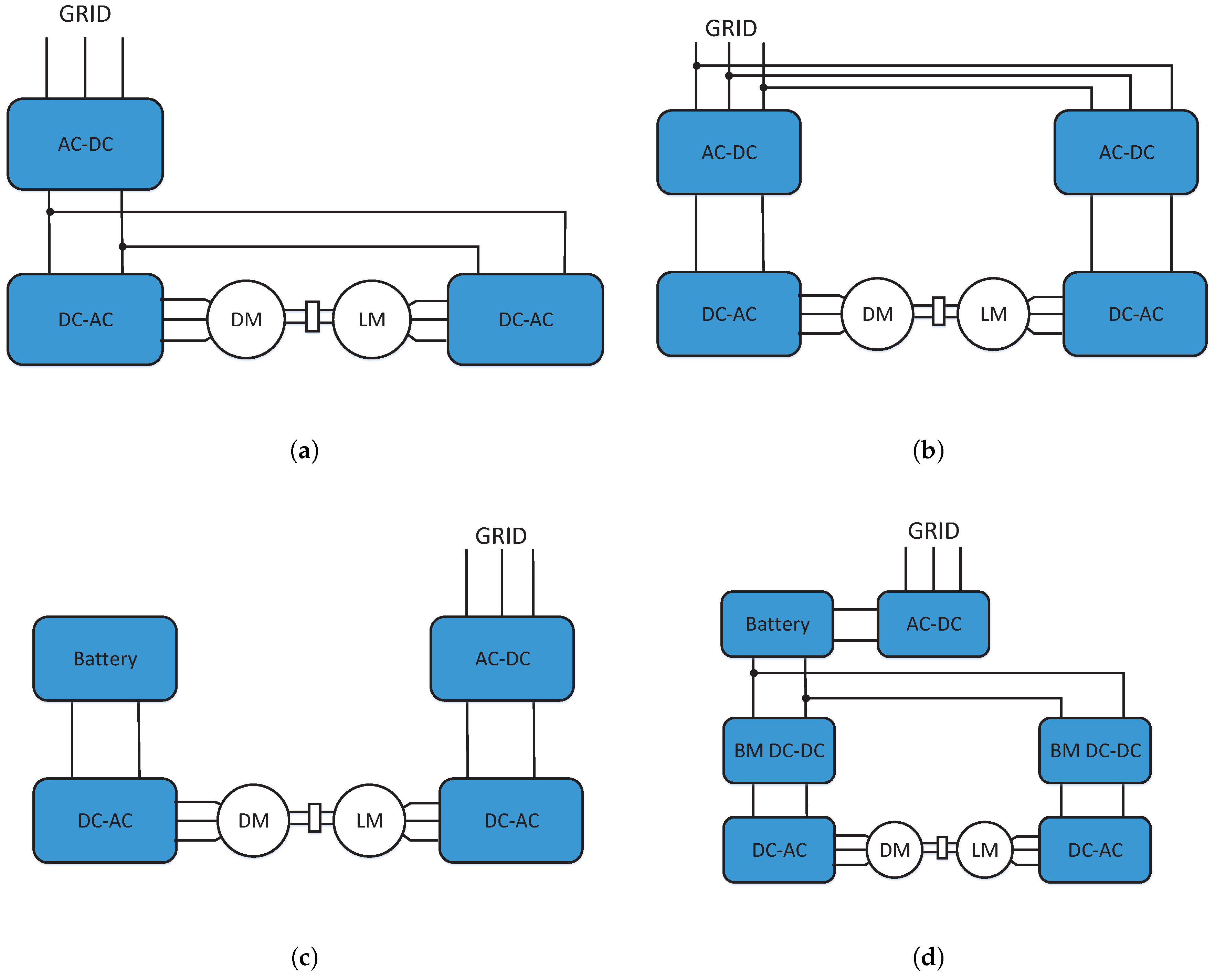
1. Introduction
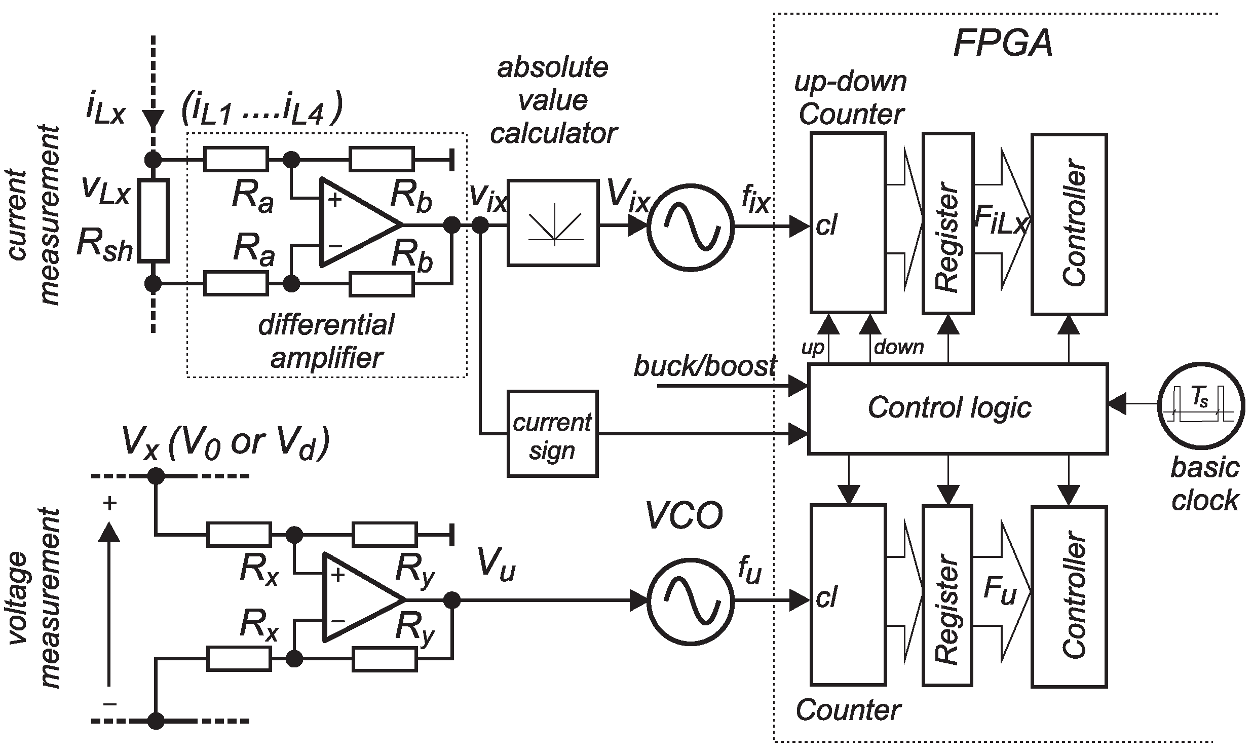
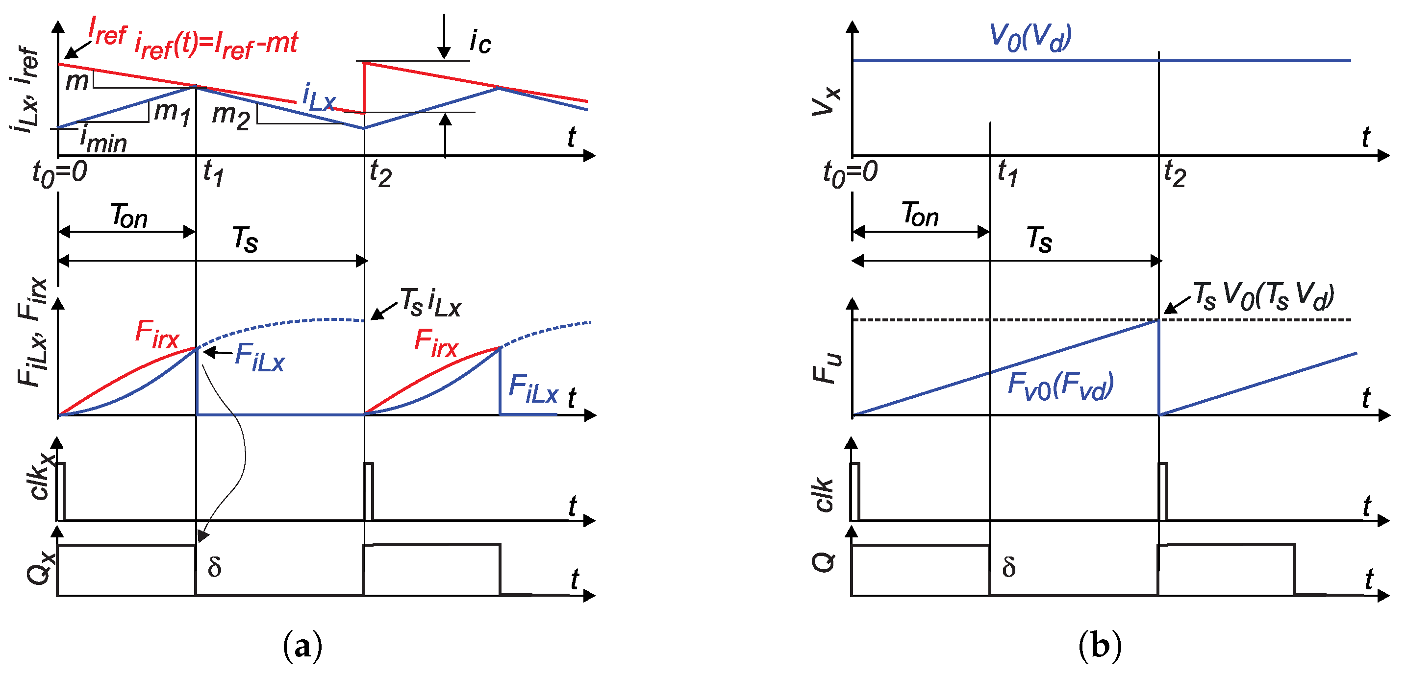
2. VCO Measurement Principle and Dynamic Reference Calculation
2.1. Analysis of Current and Voltage-Measurements
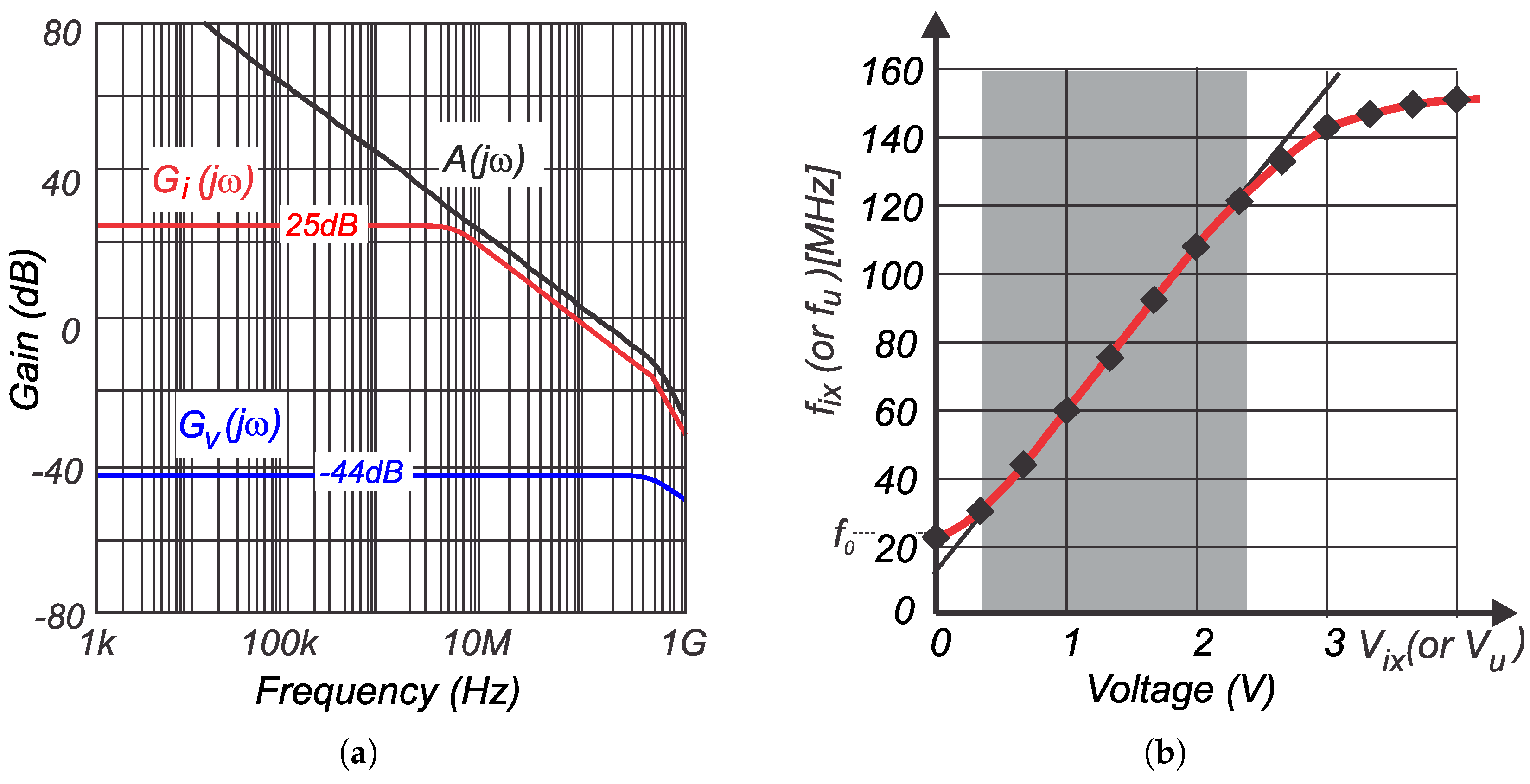
2.2. Bandwidth of the Current and Voltage Measurement Chain
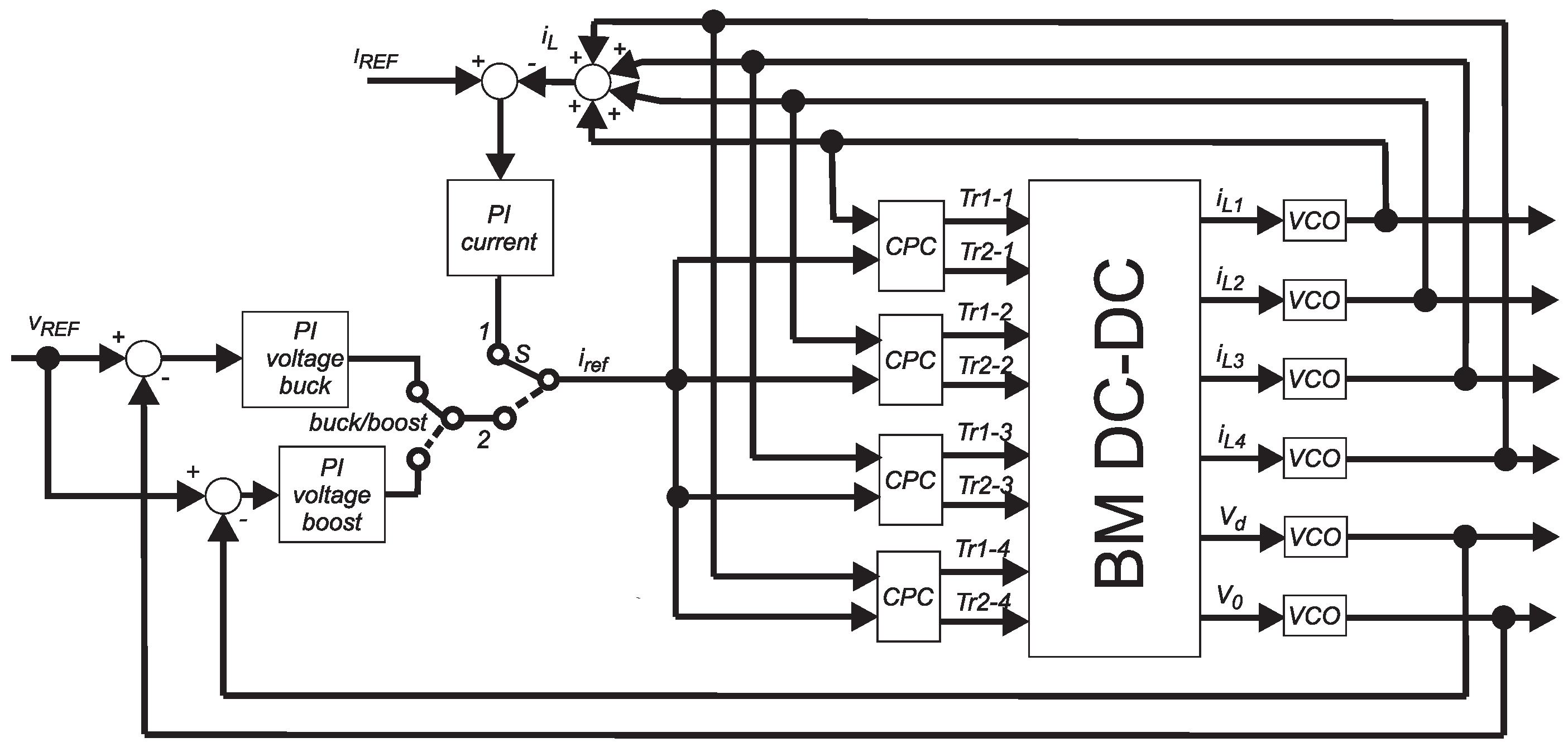
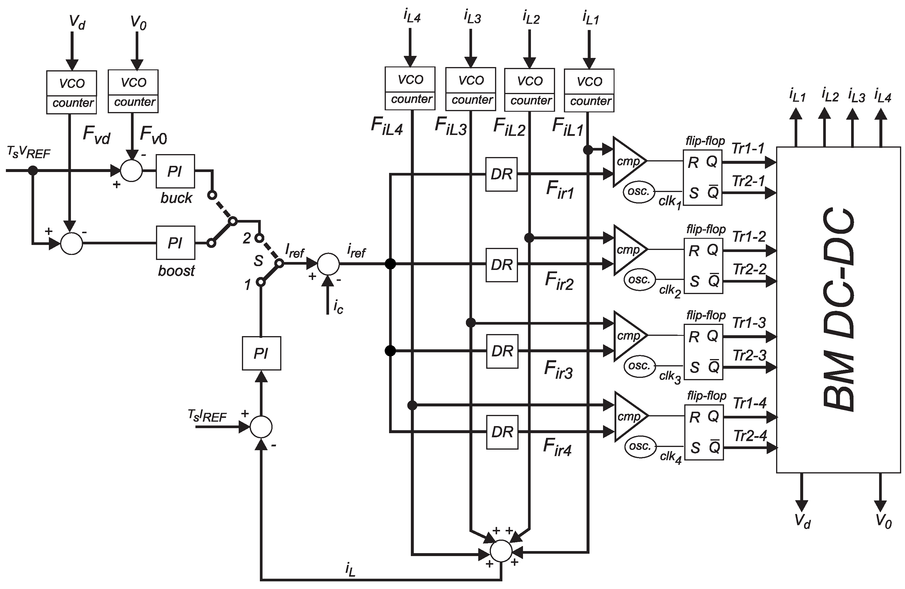
2.3. The Inductor Current Dynamic Reference (DR)
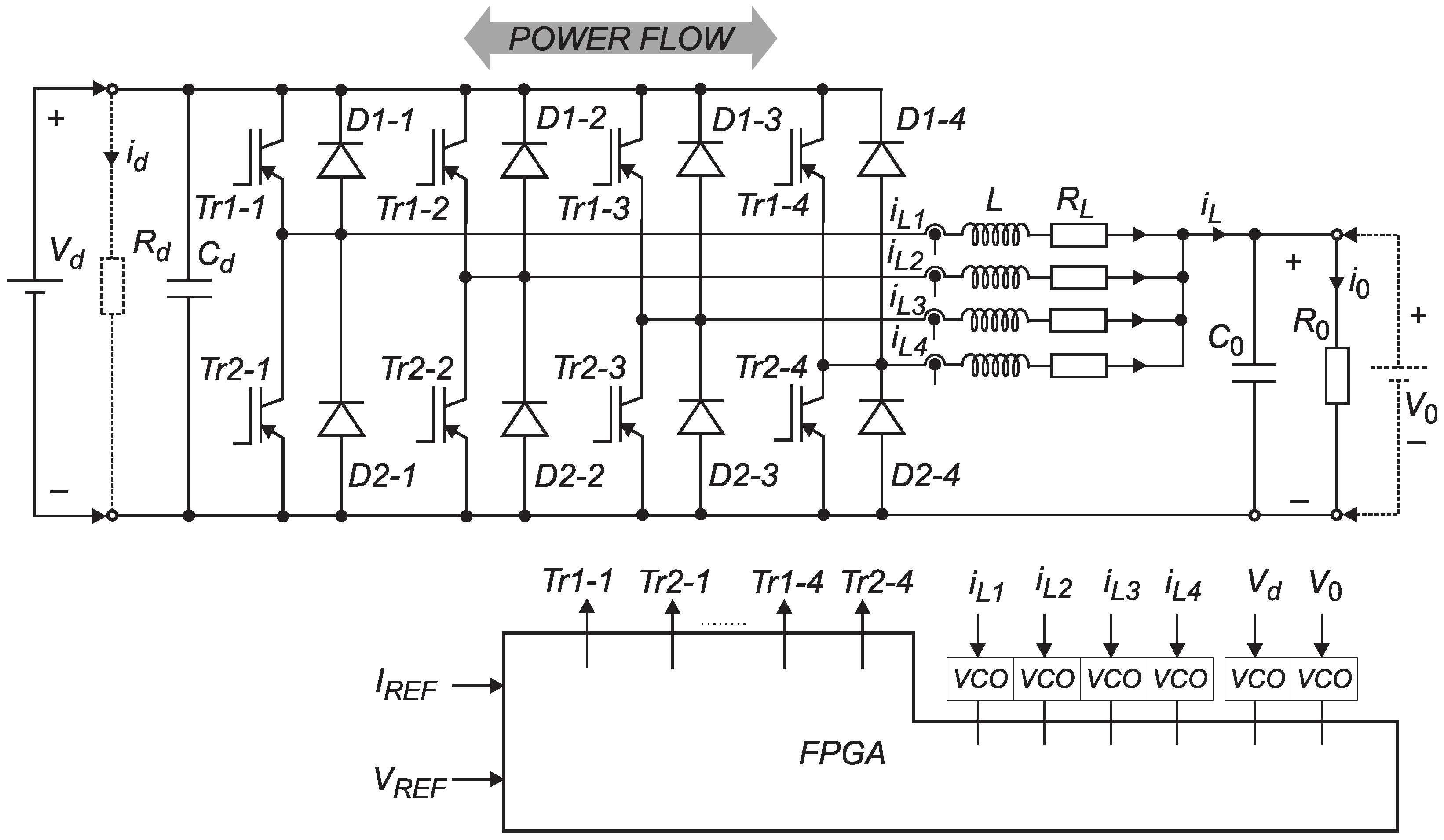
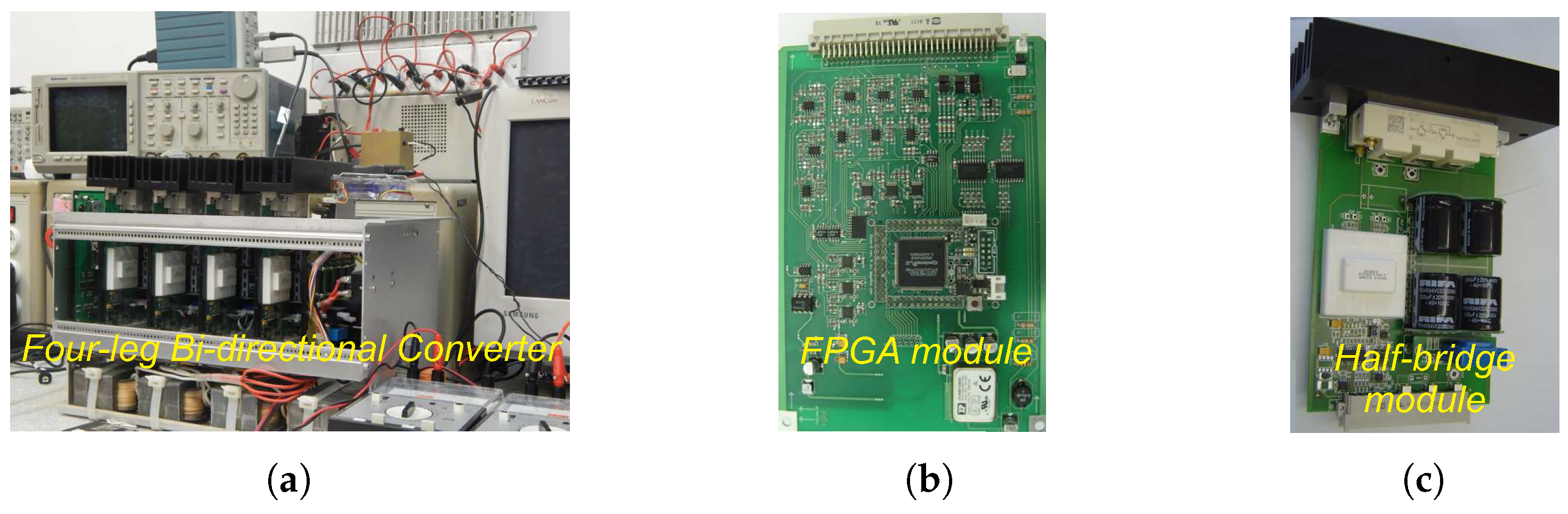
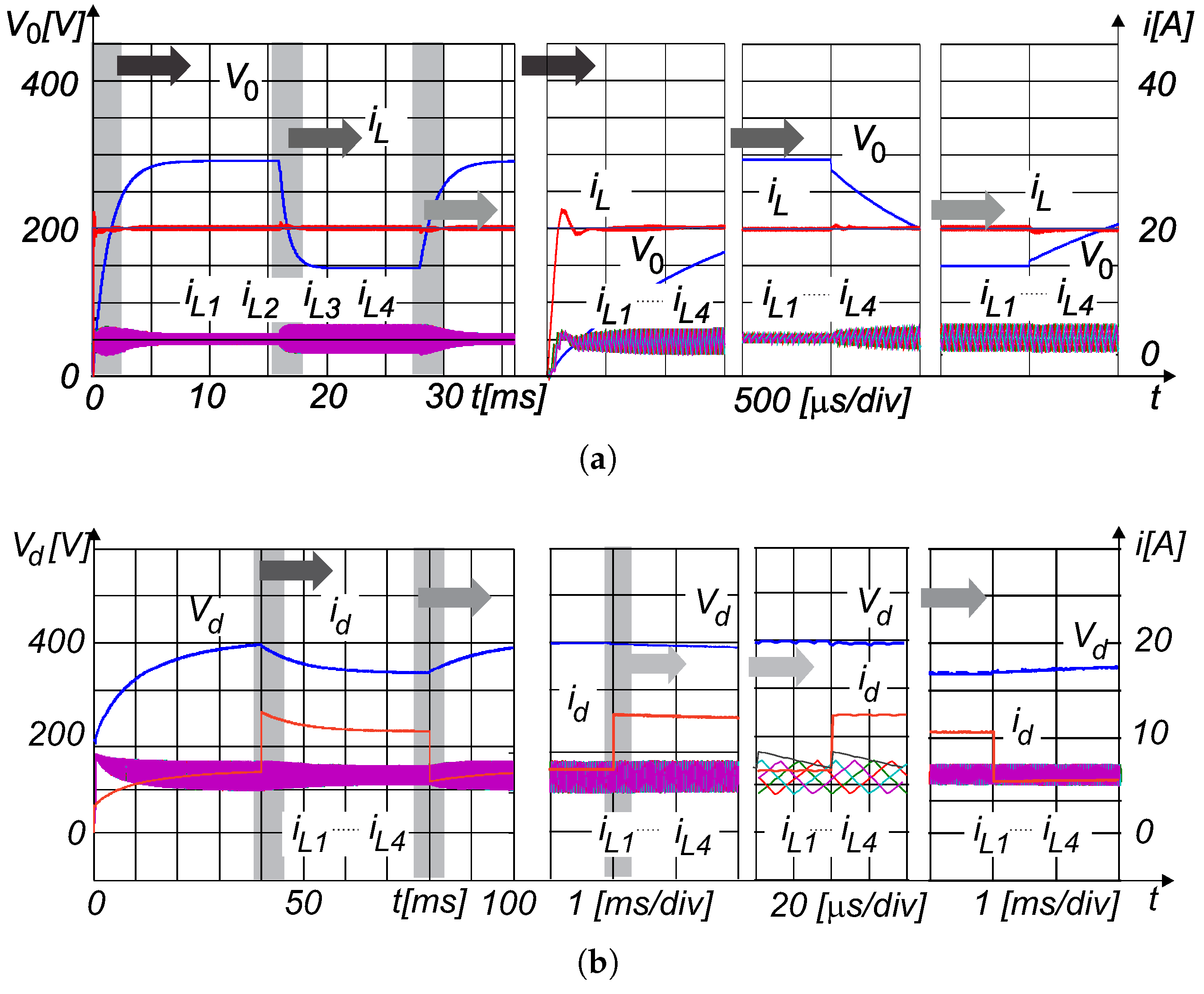
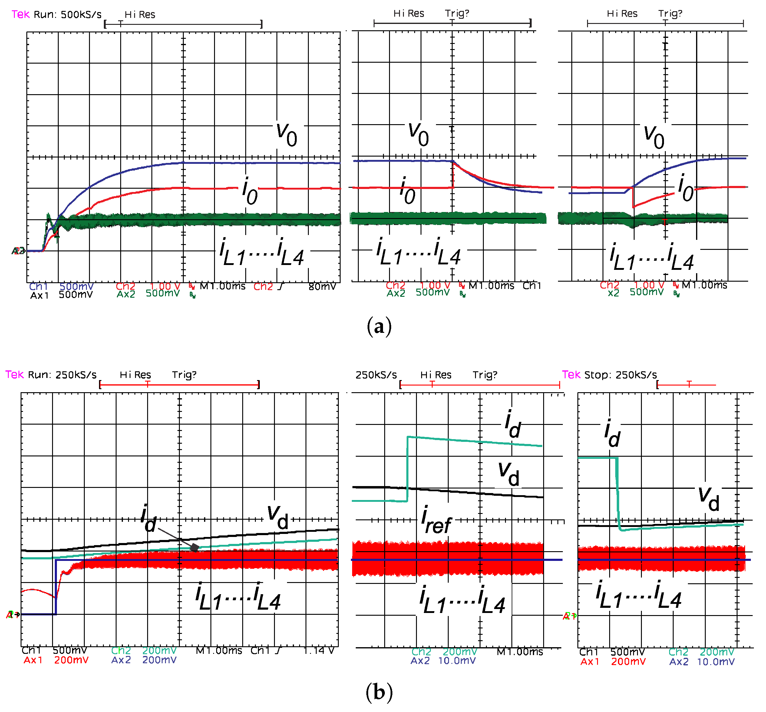
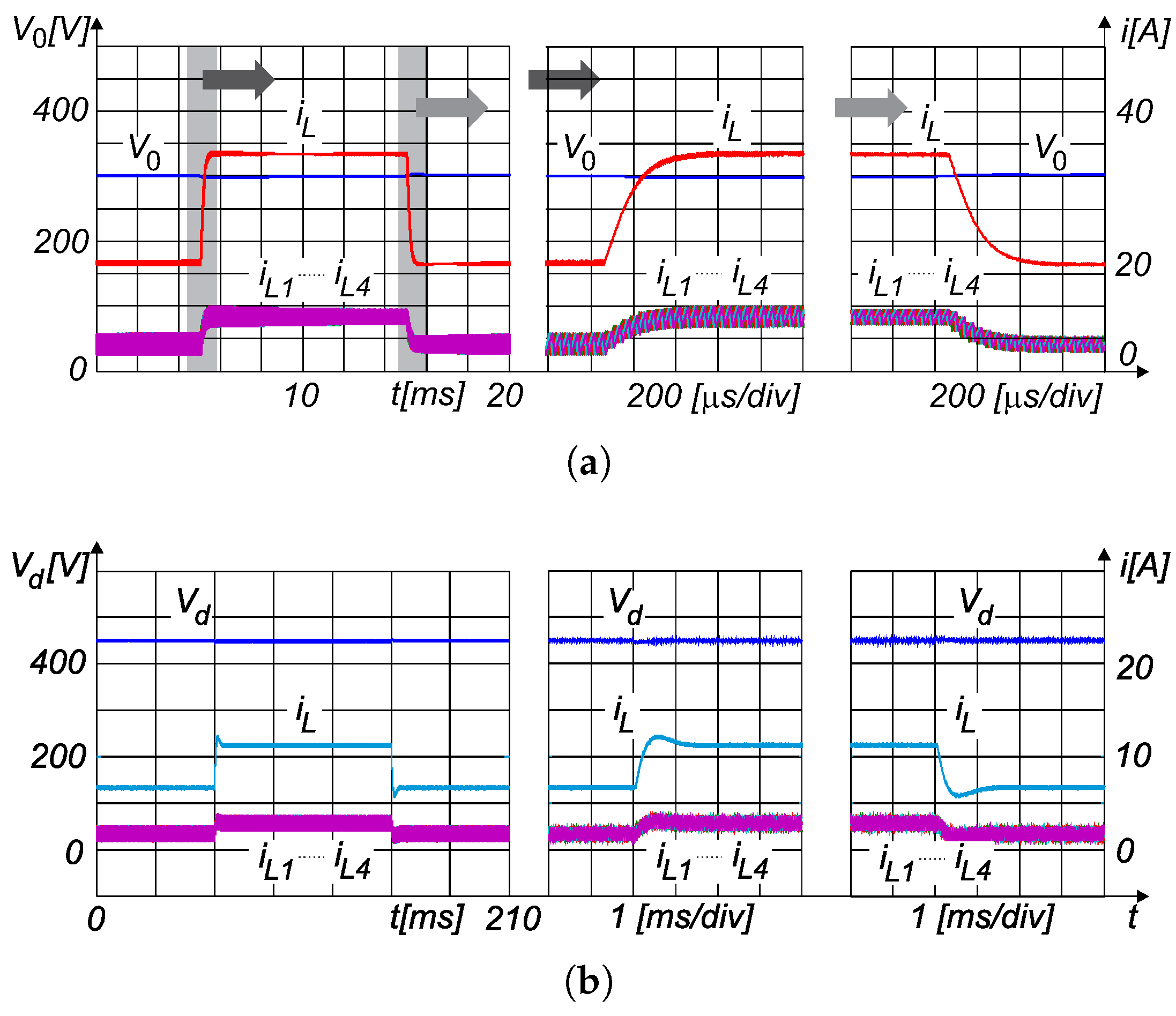
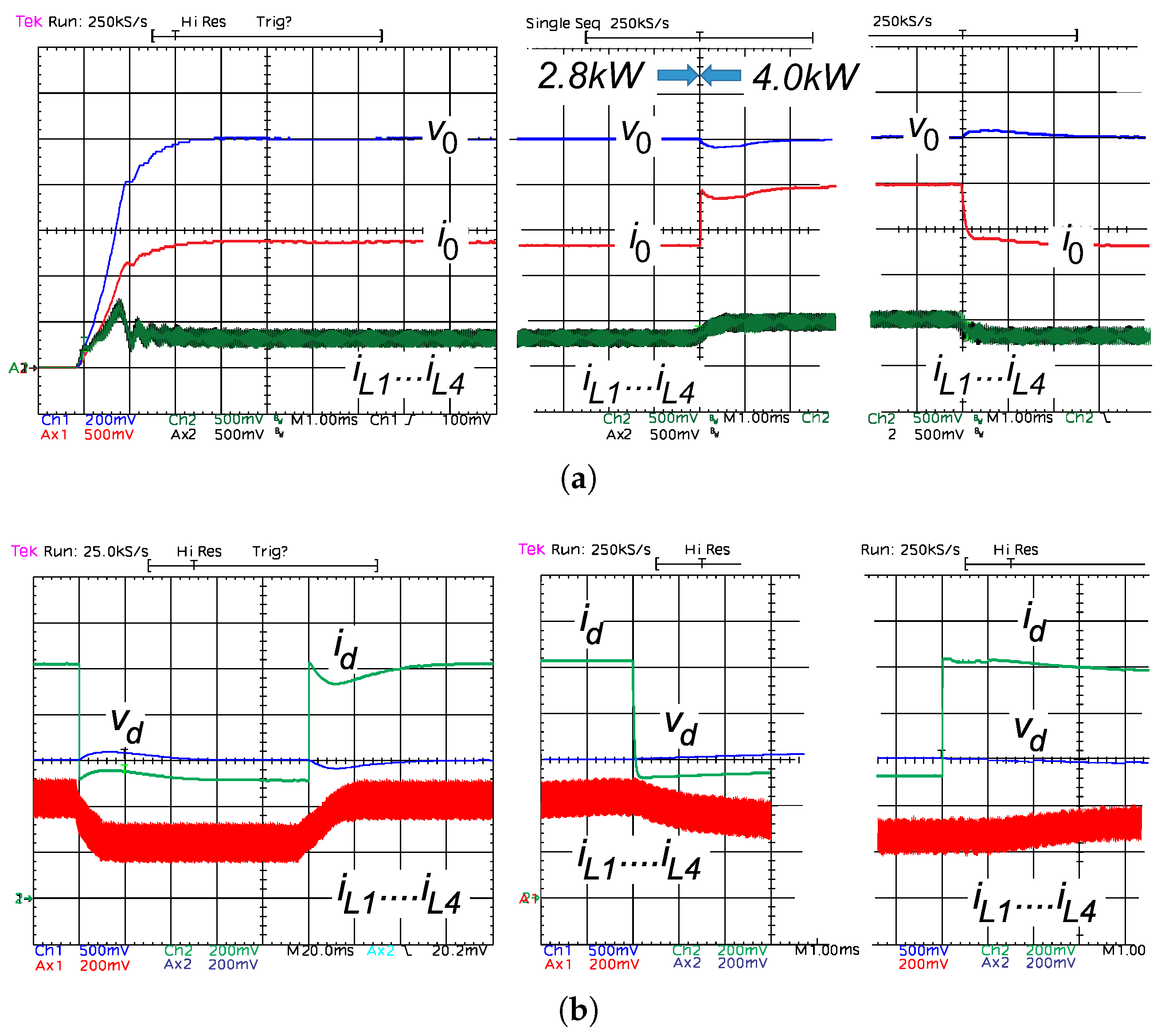
3. Simulation and Experimentation
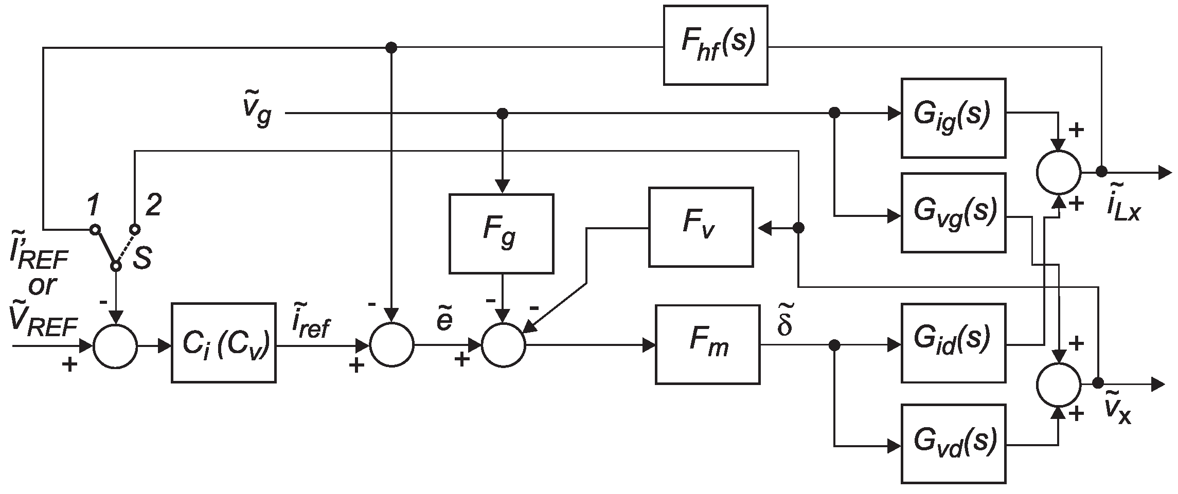
3.1. Control Scheme Model
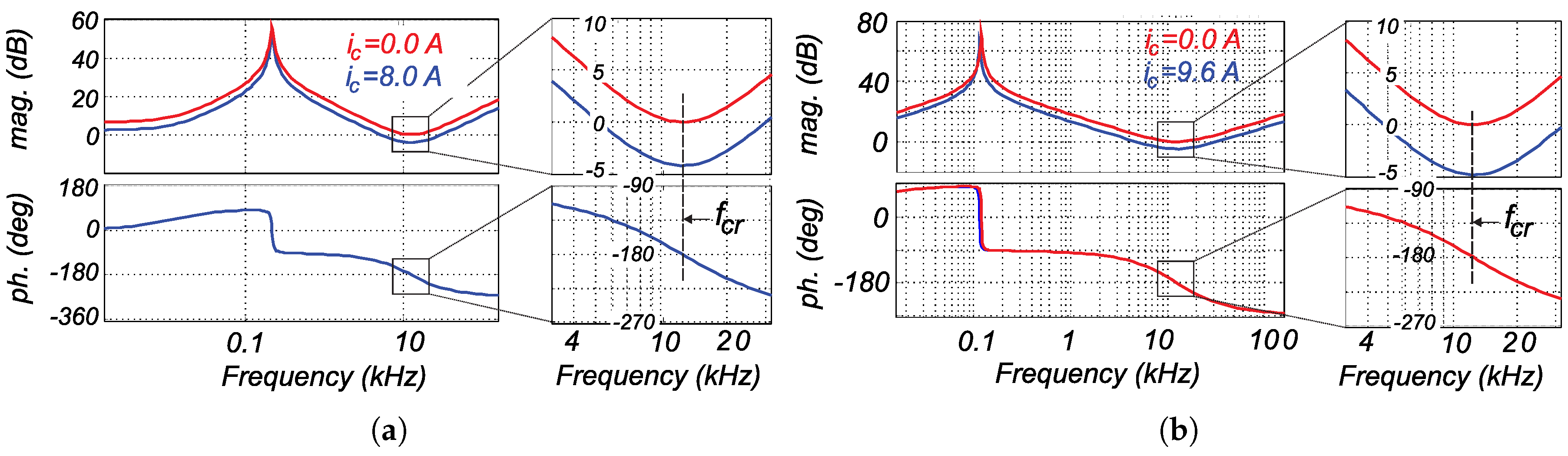
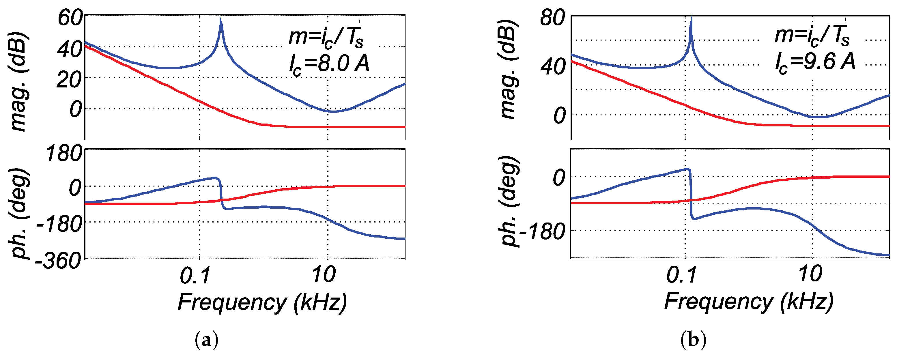
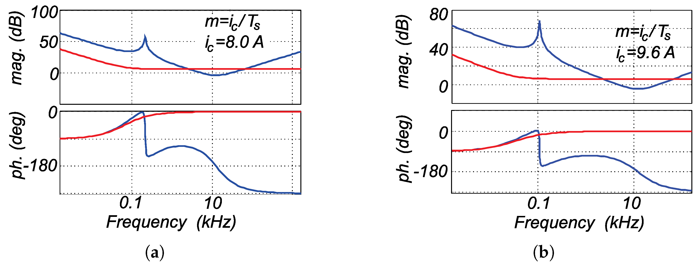
3.2. Current-Programmed Control Transfer Function
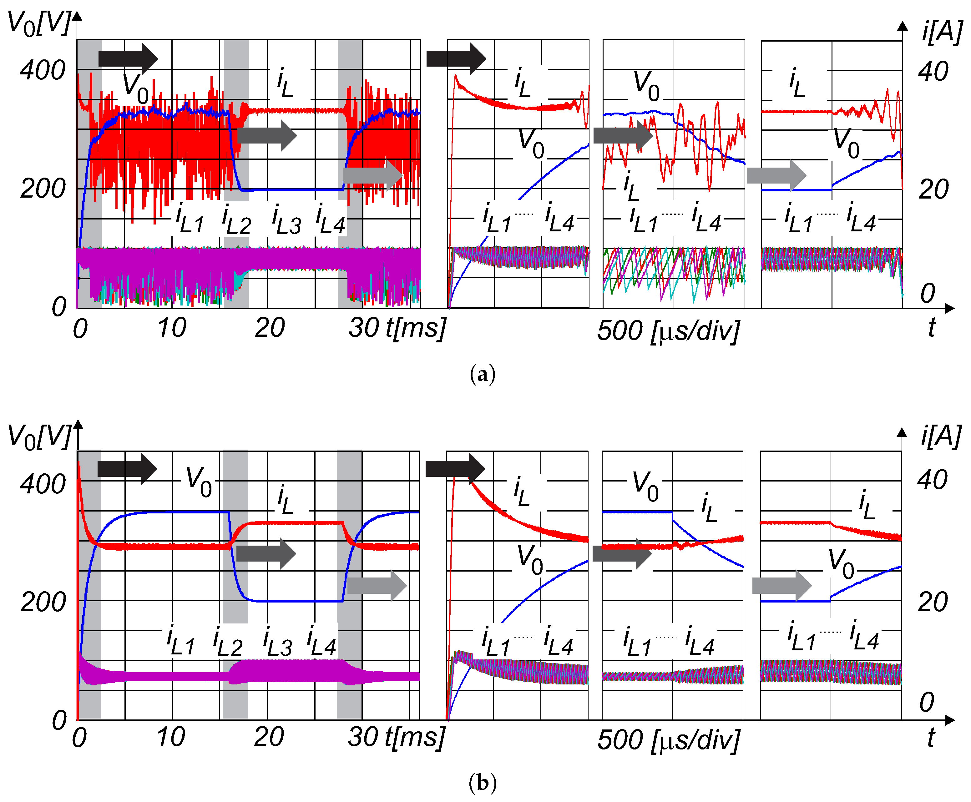
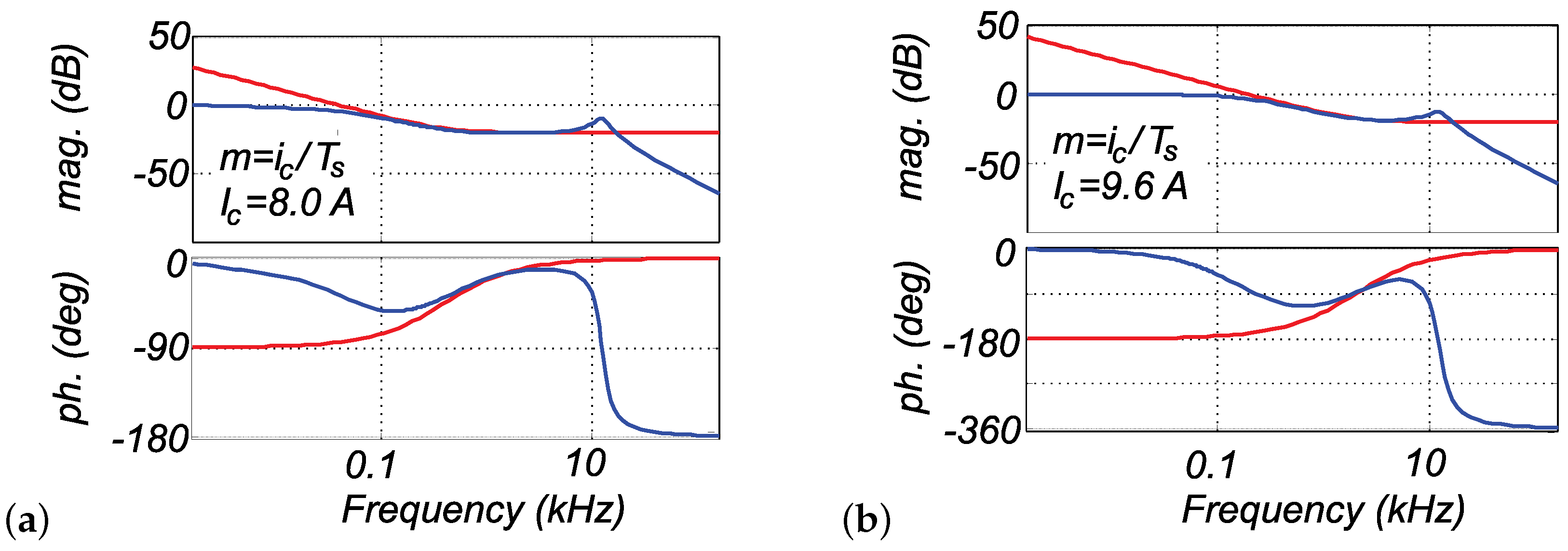
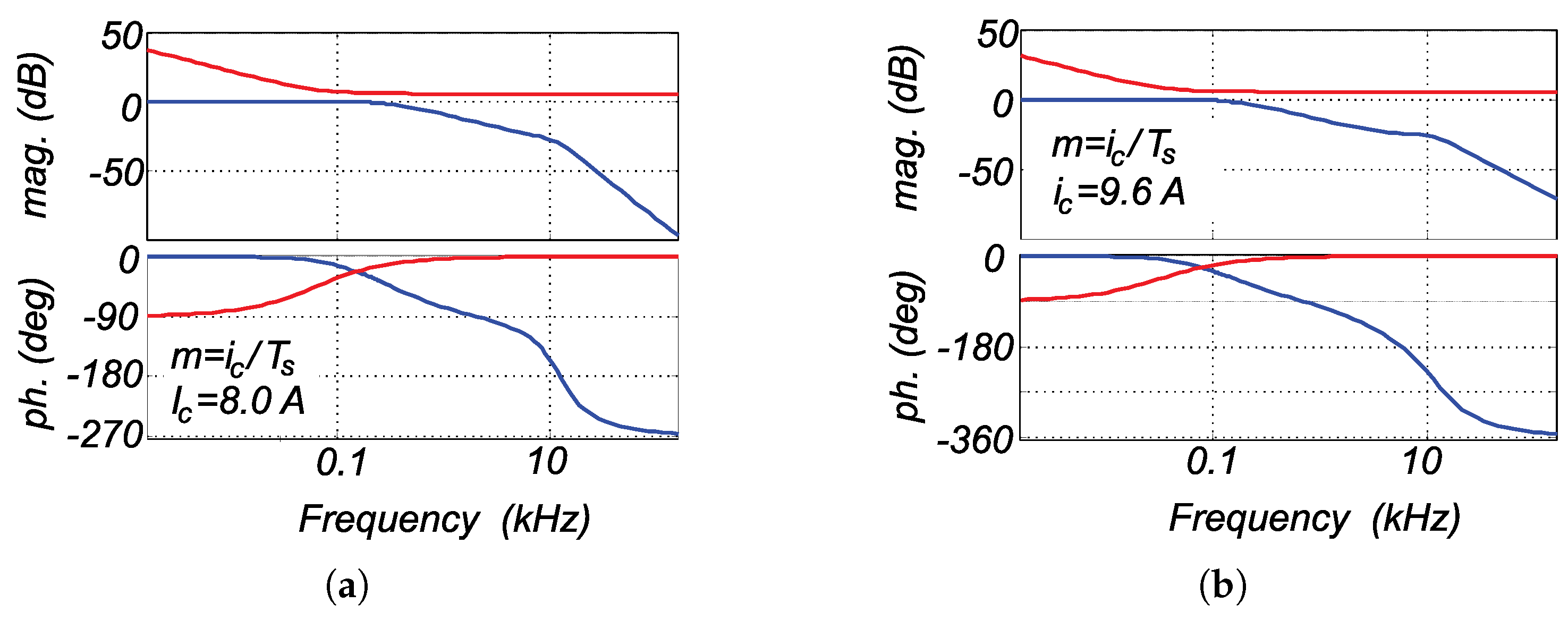
3.3. Current Control with PI Compensator
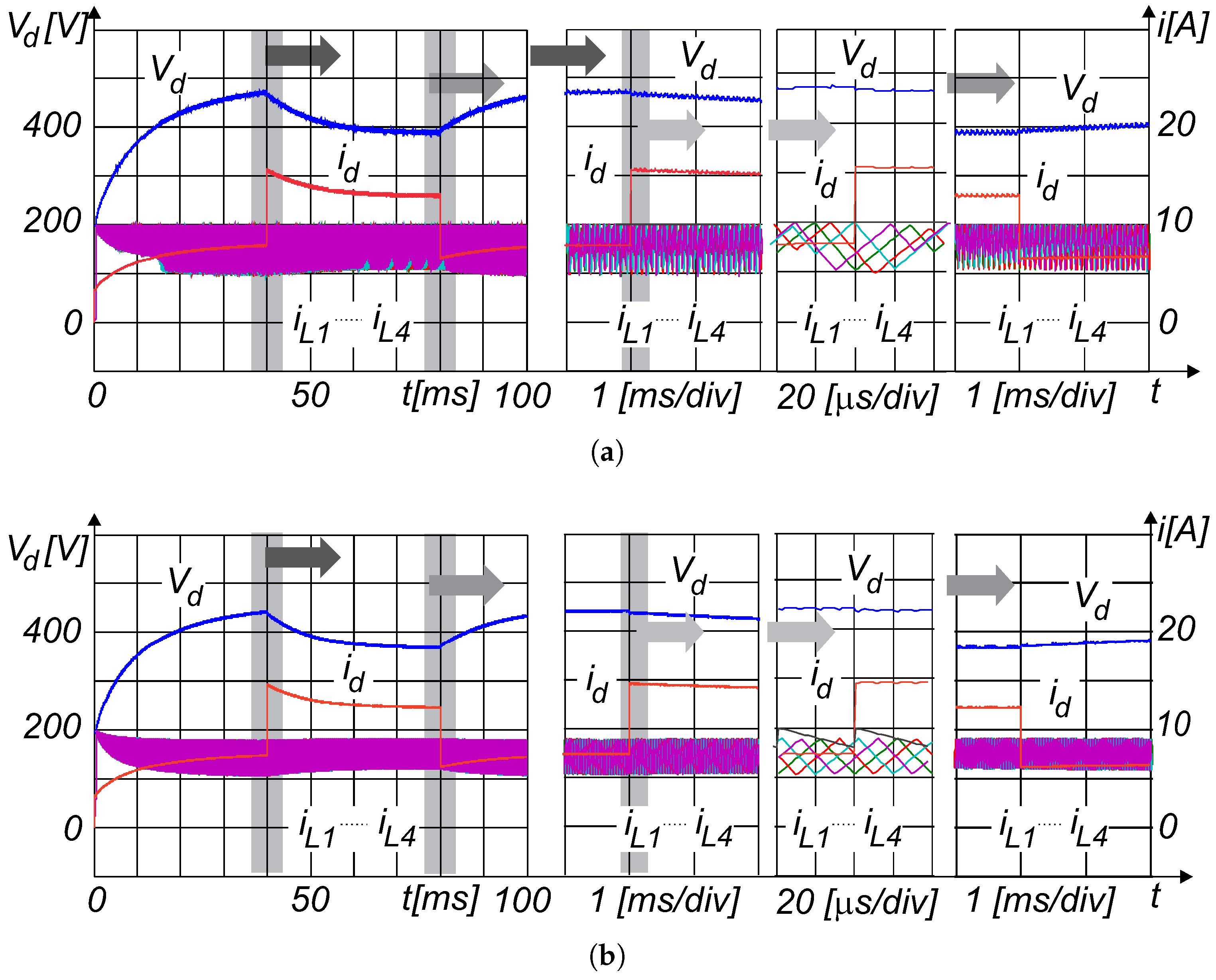
3.4. Voltage Control
4. Conclusions
Author Contributions
Funding
Conflicts of Interest
Abbreviations
| Acronyms | |
| BM DC–DC | Bi-Directional Multi-Phase DC–DC Converter |
| CCM | Continuous Current Mode |
| CPC | Current-Programmed Control (current programmed controller) |
| CR | Compensating Ramp |
| DR | Dynamic Reference |
| DSP | Digital Signal Processor |
| FPGA | Field-Programmable Gate Array |
| PI | PI compensator (controller) |
| PWM | Pulse Width Modulation |
| VCO | Voltage Control Oscillator |
| Nomenclature | |
| voltage measurement gain | |
| open-loop gain of the amplifier at the frequency Hz | |
| frequency dependent gain of the operational amplifier | |
| input capacitance | |
| current compensator (controller) transfer function | |
| voltage compensator (controller) transfer function | |
| output capacitance | |
| F | VCO output |
| current control error in small-signal model | |
| input voltage-to-duty cycle gain | |
| high-frequency term | |
| current reference in area space | |
| integral inductor current | |
| modulation gain | |
| output-voltage-to-control gain | |
| integral input voltage | |
| integral output voltage | |
| bandwidth of the current measurement chain [Hz] | |
| bandwidth of the voltage measurement chain [Hz] | |
| critical frequency for phase margin | |
| instantaneous VCO frequency () for inductor current | |
| Converter switching frequency () | |
| VCO frequency | |
| instantaneous VCO frequency for voltages | |
| free-running frequency of the VCO when V | |
| current closed-loop frequency characteristics of measurement circuit | |
| duty-cycle–to-current-output transfer function | |
| voltage-input-to-current-output transfer function | |
| closed-loop gain of the inductor current measurement circuit up to frequency | |
| voltage closed-loop frequency characteristics of measurement circuit | |
| duty-cycle-to-voltage-output transfer function | |
| voltage-input-to-voltage-output transfer function | |
| closed-loop gain of the inductor current measurement circuit up to frequency | |
| reference value of total inductor current with compensation (PI compensator) | |
| reference value of inductor current without compensation (PI compensator) | |
| reference value variation for phase current (outer control loop) | |
| total inductor current | |
| current output in small-signal model | |
| inductor current, phase x | |
| inductor current, phase 1 | |
| inductor current, phase 2 | |
| inductor current, phase 3 | |
| inductor current, phase 4 | |
| compensating current | |
| input load current | |
| current at the start of VCO operation | |
| desired value of inductor current with compensation | |
| current reference variation in small-signal model (inner control loop) | |
| output load current | |
| , | current compensator parameters |
| , | voltage compensator parameters |
| voltage VCO gain | |
| inductor current VCO gain | |
| voltage-to-frequency gain | |
| L | BM DC–DC converter phase inductance |
| m | compensating ramp slope |
| current rising slope | |
| current falling slope | |
| phase inductor resistance | |
| and | values of resistors used for current measurement |
| input load (load in boost operation) | |
| shunt resistance | |
| , and | values of resistors used for voltage measurement |
| output load (load in buck operation) | |
| converter sampling time (, PWM period | |
| time of transistor turned-on | |
| t | time |
| and | VCO integration limits |
| transistor turn-on time, current and voltage VCO are started | |
| transistor turn-off time—current VCO is read | |
| transistor switching period time—voltage VOCs are read | |
| reference voltage | |
| reference value variation for voltage (outer) control loop | |
| input voltage of BM DC–DC converter | |
| Input voltage of VCO | |
| voltage to be measured with VCO | |
| voltage drop on the shunt resistor for inductor current measurement | |
| output voltage of BM DC–DC converter | |
| voltage input in small-signal model | |
| voltage output in small-signal model | |
| duty cycle function value | |
| PWM duty cycle | |
| PWM duty cycle variation in small-signal model | |
| VCO running time | |
| frequency [rad/s] | |
| frequency where the open-loop gain of the operational amplifier is decreased by 3 dB | |
| bandwidth of the current measurement chain [rad/s] | |
| bandwidth of the voltage measurement chain [rad/s] | |
| cross-over frequency at unity open-loop gain ( [dB]) |
References
- Saponara, S. An Actuator Control Unit for Safety-Critical Mechatronic Applications with Embedded Energy Storage Backup. Energies 2016, 9, 213. [Google Scholar] [CrossRef]
- IEC/ISO. Functional Safety of Electrical/Electronic/Programmable Electronic Safety-Related Systems; IEC 61508 Parts 1–7, 2nd ed. 4/2010; IEC: Geneva, Switzerland, 2010. [Google Scholar]
- ISO 26262:2011. Road Vehicles-Functional Safety; International Organisation for Standardisation; ISO: Geneva, Switzerland, 2011. [Google Scholar]
- Newton, R.W.; Betz, R.E.; Penfold, H.B. Emulating Dynamic Load Characteristic Using a Dynamic Dynamometer. In Proceedings of the IEEE Power Electronics and Drive Systems (PEDS), Singapore, 21–24 February 1995; pp. 465–470. [Google Scholar]
- Akpolat, Z.H.; Asher, G.M.; Clare, J.C. Dynamic Emulation of Mechanical Loads Using a Vector Controlled Induction Motor-Generator Set. IEEE Trans. Ind. Electr. 1999, 46, 370–379. [Google Scholar] [CrossRef]
- Rodič, M.; Jezernik, K.; Trlep, M. Feedforward and feedback approach for the dynamic emulation of mechanical loads. In Proceedings of the Symposium on Power Electronics, Electrical Drives, Automation and Motion, Capry, Italy, 16–18 June 2004; pp. 555–560. [Google Scholar]
- Bose, B.K. Power Electronics and Motor Drives: Advances and Trends; Elsevier Inc.: New York, NY, USA, 2006. [Google Scholar]
- Shabestari, P.M.; Ziaeinejad, S.; Mehrizi-Sani, A. Reachability analysis for a grid-connected voltage-sourced converter (VSC). In Proceedings of the IEEE Applied Power Electronics Conference and Exposition (APEC), San Antonio, TX, USA, 4–8 March 2018; pp. 2349–2354. [Google Scholar]
- Trzynadlowski, A.M. Introduction to Modern Power Electronics; Wiley: New York, NY, USA, 1998. [Google Scholar]
- Adam, G.P.; Anaya-Lara, O.; Burt, G.; Mconald, J.R. Comparison between flying capacitor and modular multilevel inverter. In Proceedings of the 35th Annual Conference of the IEEE Industrial Electronics Society, Porto, Portugal, 3–5 November 2009. [Google Scholar]
- Miceli, R.; Schettino, G.; Viola, F. A Novel Computational Approach for Harmonic Mitigation in PV Systems with Single-Phase Five-Level CHBMI. Energies 2018, 11, 2100. [Google Scholar] [CrossRef]
- Hoon, Y.; Mohd Radzi, M.A.; Hassan, M.K.; Mailah, N.F. Control Algorithms of Shunt Active Power Filter for Harmonics Mitigation: A Review. Energies 2017, 10, 2038. [Google Scholar] [CrossRef]
- Zhang, C.; Guo, Q.; Li, L.; Wang, M.; Wang, T. System Efficiency Improvement for Electric Vehicles Adopting a Permanent Magnet Synchronous Motor Direct Drive System. Energies 2017, 10, 2030. [Google Scholar] [CrossRef]
- Yu, F.; Cheng, M.; Chau, K.T.; Li, F. Control and Performance Evaluation of Multiphase FSPM Motor in Low-Speed Region for Hybrid Electric Vehicles. Energies 2015, 8, 10335–10353. [Google Scholar] [CrossRef]
- Mousavi Sangdehi, S.M.; Hamidifar, S.; Kar, N.C. A Novel Bidirectional DC/AC Stacked Matrix Converter Design for Electrified Vehicle Applications. IEEE Trans. Veh. Technol. 2014, 63, 3038–3050. [Google Scholar] [CrossRef]
- Zhang, Z.; Ge, X.; Tian, Z.; Zhang, X.; Tang, Q.; Feng, X. A PWM for Minimum Current Harmonic Distortion in Metro Traction PMSM With Saliency Ratio and Load Angle Constrains. IEEE Trans. Power Electr. 2018, 33, 4498–4511. [Google Scholar] [CrossRef]
- Pillay, P.; Krishnan, R. Modeling, simulation, and analysis of permanent-magnet motor drives. I. The permanent-magnet synchronous motor drive. IEEE Trans. Ind. Appl. 1989, 25, 265–273. [Google Scholar] [CrossRef]
- Garcia, O.; Zumel, P.; de Castro, A.; Cobos, A. Automotive DC-DC bidirectional converter made with many interleaved buck stages. IEEE Trans. Power Electr. 2016, 21, 578–586. [Google Scholar] [CrossRef]
- Xue, L.-K.; Wang, P.; Wang, Y.-F.; Bei, T.-Z.; Yan, H.-Y. A Four-Phase High Voltage Conversion Ratio Bidirectional DC-DC Converter for Battery Applications. Energies 2015, 8, 6399–6426. [Google Scholar] [CrossRef]
- Long, B.; Jeong, T.W.; Deuk Lee, J.; Jung, Y.C.; Chong, K.T. Energy Management of a Hybrid AC–DC Micro-Grid Based on a Battery Testing System. Energies 2015, 8, 1181–1194. [Google Scholar] [CrossRef]
- Vidal-Idiarte, E.; Martnez-Salamero, L.; Guinjoan, F.; Calvente, J.; Gomariz, S. Sliding and fuzzy control of a boost converter using an 8-bit microcontroller. IEE Proc. Electr. Power Appl. 2004, 151, 5–11. [Google Scholar] [CrossRef]
- Simon-Muela, A.; Petibon, S.; Alonso, C.; Chaptal, J.L. Practical implementation of a high-frequency current-sense technique for VRM. IEEE Trans. Ind. Electr. 2008, 55, 3221–3230. [Google Scholar] [CrossRef]
- Kurokawa, F.; Kajiwara, K. A New Digital Average Current-Injected Control DC-DC Converter Using VCO. In Proceedings of the International Conference on Electrical Machines and Systems (ICEMS), Beijing, China, 20–23 August 2011. [Google Scholar]
- Qiu, Y.; Liu, H.; Chen, X. Digital Average Current-Mode Control of PWM DC-DC Converters without Current Sensors. IEEE Trans. Ind. Electr. 2010, 57, 1670–1677. [Google Scholar]
- Liu, K.-B.; Liu, C.-Y.; Liu, Y.-H.; Chien, Y.-C.; Wang, B.-S.; Wong, Y.-S. Analysis and Controller Design of a Universal Bidirectional DC-DC Converter. Energies 2016, 9, 501. [Google Scholar] [CrossRef]
- Nguyen, D.-D.; Nguyen, D.-H.; Funabashi, T.; Fujita, G. Sensorless Control of Dual-Active-Bridge Converter with Reduced-Order Proportional-Integral Observer. Energies 2018, 11, 931. [Google Scholar] [CrossRef]
- Tahir, S.; Wang, J.; Baloch, M.; Kaloi, G. Digital Control Techniques Based on Voltage Source Inverters in Renewable Energy Applications: A Review. Electronics 2018, 7, 18. [Google Scholar] [CrossRef]
- Liu, Y.; Yin, S.; Pan, X.; Wang, H.; Wang, G.; Peng, J. Effects of Nonlinearity in Input Filter on the Dynamic Behavior of an Interleaved Boost PFC Converter. Energies 2017, 10, 1530. [Google Scholar] [CrossRef]
- Gow, J.A.; Manning, C.D. Novel fast-acting predictive current mode controller for power electronic converters. IEE Proc. Electr. Power Appl. 2001, 148, 133–139. [Google Scholar] [CrossRef]
- Matsuo, H.; Kurokawa, F.; Asano, M. Over-current Limiting Characteristics of the DC-DC Converter with a New Digital Current-Injected Control Circuit. IEEE Trans. Power Electr. 1998, 13, 645–650. [Google Scholar] [CrossRef]
- Kurokawa, F.; Sukita, S. A New Model Control DC-DC Converter to Improve Dynamic Characteristics. In Proceedings of the IEEE PEDS, Bangkok, Thailand, 27–30 November 2007; pp. 763–767. [Google Scholar]
- Vorperian, V. Simplified Analaysis of PWM Converters using the Model of PWM switch Part I: Continuous Conduction Mode. Trans. Aerosp. Electr. Syst. 1990, 26, 490–596. [Google Scholar] [CrossRef]
- Vorperian, V. Simplified Analaysis of PWM Converters using the Model of PWM switch Part II: Discontinuous Conduction Mode. Trans. Aerosp. Electr. Syst. 1990, 26, 497–505. [Google Scholar] [CrossRef]
- Ridley, R.B. A New Small-Signal Model for Current Mode Control. Ph.D. Thesis, Virginia Polytechnic Institute and State University, Blacksburg, VA, USA, 1990. [Google Scholar]
- Texas Instruments, LMH6611: Single Supply 345 MHz Rail-to-Rail Output Amplifiers. Texas Instruments, 2013. Available online: http://www.ti.com/lit/ds/symlink/lmh6611.pdf (accessed on 31 July 2018).
- Sedra, A.S.; Smith, K.C. Microelectronic Circuits, 6th ed.; Oxford Series in Electrical & Computer Engineering; Oxford University Press: Oxford, UK, 2009. [Google Scholar]
- Erickson, R.W.; Maksimovič, D. Fundamentals of Power Electronics; Kluwer Academic Publishers Group: New York, NY, USA, 2001. [Google Scholar]
- Truntič, M.; Milanovič, M. Voltage and current-mode control for a buck-converter based on measured integral values of voltage and current implemented in FPGA. IEEE Trans. Power Electr. 2014, 29, 6686–6699. [Google Scholar] [CrossRef]


| Buck Conversion | ||||
| Input | Output | Load | ||
| up to 500 V | 200 to 300 V | 620 H | 880 F | |
| Boost Conversion | ||||
| Input | Output | Load | ||
| up to 300 V | 350 to 500 V | 620 H | 880 F |
| Buck | ||
| Boost | ||
| , |
| Buck | |||
| Boost | |||
© 2018 by the authors. Licensee MDPI, Basel, Switzerland. This article is an open access article distributed under the terms and conditions of the Creative Commons Attribution (CC BY) license (http://creativecommons.org/licenses/by/4.0/).
Share and Cite
Rodič, M.; Milanovič, M.; Truntič, M. Digital Control of an Interleaving Operated Buck-Boost Synchronous Converter Used in a Low-Cost Testing System for an Automotive Powertrain. Energies 2018, 11, 2290. https://doi.org/10.3390/en11092290
Rodič M, Milanovič M, Truntič M. Digital Control of an Interleaving Operated Buck-Boost Synchronous Converter Used in a Low-Cost Testing System for an Automotive Powertrain. Energies. 2018; 11(9):2290. https://doi.org/10.3390/en11092290
Chicago/Turabian StyleRodič, Miran, Miro Milanovič, and Mitja Truntič. 2018. "Digital Control of an Interleaving Operated Buck-Boost Synchronous Converter Used in a Low-Cost Testing System for an Automotive Powertrain" Energies 11, no. 9: 2290. https://doi.org/10.3390/en11092290
APA StyleRodič, M., Milanovič, M., & Truntič, M. (2018). Digital Control of an Interleaving Operated Buck-Boost Synchronous Converter Used in a Low-Cost Testing System for an Automotive Powertrain. Energies, 11(9), 2290. https://doi.org/10.3390/en11092290